

Page 1

PAMS Technical Documentation
RAE–2 Series Transceiver
Chapter 1
GENERAL
INFORMATION
Original 02/99
Copyright 1999 Nokia Mobile Phones. All rights reserved.
Page 2
RAE–2
PAMS
General Information
Amendment
Number
Technical Documentation
AMENDMENT RECORD SHEET
Date Inserted By Comments
01/99 Original
Page 1–2
Original 02/99
Page 3

PAMS
RAE–2
Technical Documentation
CHAPTER 1 – GENERAL INFORMATION
Contents
Introduction Page 1–5. . . . . . . . . . . . . . . . . . . . . . . . . . . . . . . . . . . . . . . . . . . .
Technical Summary Page 1–5. . . . . . . . . . . . . . . . . . . . . . . . . . . . . . . . . . .
Product Selection Page 1–6. . . . . . . . . . . . . . . . . . . . . . . . . . . . . . . . . . . . . . .
Units and Accessories Page 1–7. . . . . . . . . . . . . . . . . . . . . . . . . . . . . . . .
Accessories for PC connection Page 1–7. . . . . . . . . . . . . . . . . . . . . . .
Audio Accessories Page 1–8. . . . . . . . . . . . . . . . . . . . . . . . . . . . . . . . .
Battery and Chargers Page 1–9. . . . . . . . . . . . . . . . . . . . . . . . . . . . . . .
Other Accessories Page 1–9. . . . . . . . . . . . . . . . . . . . . . . . . . . . . . . . . .
Structure Page 1–10. . . . . . . . . . . . . . . . . . . . . . . . . . . . . . . . . . . . . . . . . . . .
List of Modules Page 1–10. . . . . . . . . . . . . . . . . . . . . . . . . . . . . . . . . . . .
Basic Specifications Page 1–11. . . . . . . . . . . . . . . . . . . . . . . . . . . . . . . .
Type Labels Page 1–12. . . . . . . . . . . . . . . . . . . . . . . . . . . . . . . . . . . . . . . . .
Keymat Variants Page 1–13. . . . . . . . . . . . . . . . . . . . . . . . . . . . . . . . . . . . . .
General Information
Technical Specifications Page 1–16. . . . . . . . . . . . . . . . . . . . . . . . . . . . . . . . .
Modes of Operation Page 1–16. . . . . . . . . . . . . . . . . . . . . . . . . . . . . . . . . . .
Electrical Specifications Page 1–16. . . . . . . . . . . . . . . . . . . . . . . . . . . . . . .
DC Characteristics Page 1–16. . . . . . . . . . . . . . . . . . . . . . . . . . . . . . . . .
Average Current Consumption Page 1–16. . . . . . . . . . . . . . . . . . . . .
AC Characteristics Page 1–16. . . . . . . . . . . . . . . . . . . . . . . . . . . . . . . . .
EL Characteristics, PDA and CMT Page 1–16. . . . . . . . . . . . . . . . .
Main RF Characteristics Page 1–17. . . . . . . . . . . . . . . . . . . . . . . . . .
Interconnection Diagram Page 1–18. . . . . . . . . . . . . . . . . . . . . . . . . .
External connections and signals Page 1–19. . . . . . . . . . . . . . . . . . . . .
List of external connectors Page 1–19. . . . . . . . . . . . . . . . . . . . . . . .
Battery Connector Page 1–20. . . . . . . . . . . . . . . . . . . . . . . . . . . . . . .
System Connector Page 1–21. . . . . . . . . . . . . . . . . . . . . . . . . . . . . . .
MMC Connector Page 1–23. . . . . . . . . . . . . . . . . . . . . . . . . . . . . . . . .
Mechanical Characteristics Page 1–24. . . . . . . . . . . . . . . . . . . . . . . . . .
User Interface specifications Page 1–25. . . . . . . . . . . . . . . . . . . . . . . . . . .
User Interface Features Page 1–25. . . . . . . . . . . . . . . . . . . . . . . . . . . . .
Temperature and Environmental Conditions Page 1–26. . . . . . . . . . .
Warnings and Restrictions Page 1–26. . . . . . . . . . . . . . . . . . . . . . . . . . .
Functional Description Page 1–27. . . . . . . . . . . . . . . . . . . . . . . . . . . . . . . . . . .
Block Diagram Page 1–27. . . . . . . . . . . . . . . . . . . . . . . . . . . . . . . . . . . . . . .
PDA Module Page 1–28. . . . . . . . . . . . . . . . . . . . . . . . . . . . . . . . . . . . . . .
CMT Module Page 1–28. . . . . . . . . . . . . . . . . . . . . . . . . . . . . . . . . . . . . .
Power Distribution Page 1–29. . . . . . . . . . . . . . . . . . . . . . . . . . . . . . . . . .
Audio Page 1–29. . . . . . . . . . . . . . . . . . . . . . . . . . . . . . . . . . . . . . . . . . . . .
Software Specifications of Interfaces Page 1–30. . . . . . . . . . . . . . . . . . . .
Original 02/99
Page 1–3
Page 4

RAE–2
PAMS
General Information
External Devices Page 1–30. . . . . . . . . . . . . . . . . . . . . . . . . . . . . . . . . . .
Interfaces Between Transceiver Processors Page 1–30. . . . . . . . . . .
Software–Hardware Interface Page 1–30. . . . . . . . . . . . . . . . . . . . . . . .
Alignment Page 1–31. . . . . . . . . . . . . . . . . . . . . . . . . . . . . . . . . . . . . . . . . . .
Flashing Page 1–32. . . . . . . . . . . . . . . . . . . . . . . . . . . . . . . . . . . . . . . . . .
Vocabulary Page 1–32. . . . . . . . . . . . . . . . . . . . . . . . . . . . . . . . . . . . . . . .
Technical Documentation
Page 1–4
Original 02/99
Page 5
PAMS
RAE–2
Technical Documentation
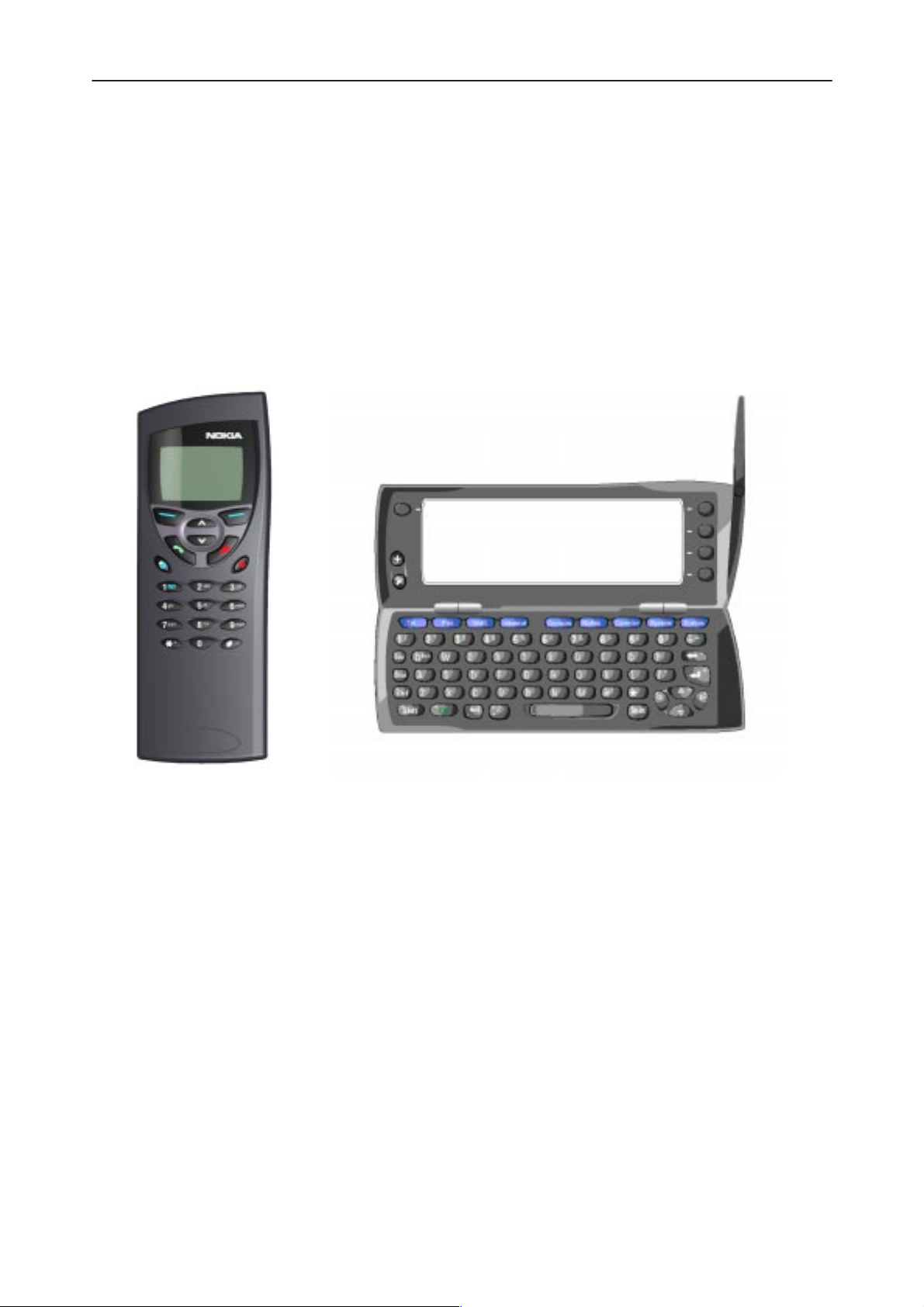
Introduction
RAE–2N is the 2nd generation communicator for GSM 900 network. Communicator extends the basic digital cellular phone with in–built data capabilities and
applications.
RAE –2 is a phase 2, class4 transceiver with 2W peak TX power.
The device has two user interfaces. The conventional phone interface on the
front cover. By opening the device the user can access the graphical user interface which can utilize the full communicator functionality.
General Information
Technical Summary
The Communicator is divided into two main domains: phone and personal digital assistant (PDA). Phone manages speech and data connections to GSM network. It also handles audio input and output. PDA runs all the applications (e.g.
calendar, contact database etc...) and utilizes the data connections made by
the phone.
The phone is based on DCT3 technology and CUI style user interface software. PDA uses AMD’s 486 CPU and GEOS operating system.
Battery technology is Li–ion.
The product has earpiece for conventional phone use but it also has an internal
handsfree speaker.
Connection to the other devices can be handled with 115kbps serial cable or
115kbps IR. Product is IrDA compatible.
Original 02/99
Page 1–5
Page 6
RAE–2
PAMS
General Information
The phone display is graphical, transflective FSTN LCD display. Display resolution is 84x48 pixels. The PDA display is graphical, transflective FSTN LCD display. Display resolution is 640x200 pixels and dot pitch is 0.17mm. Contrast is
good enough to show 16 gray scales.
Both LCD displays are backlit with EL–panel.
In addition to the fixed memory the product can use memory extension module,
MMC, to expand the user file system area. The MMC supports hot insertion.
NOTE: Due to the infrared data link the RAE–2 is officially specificed as :
CLASS 1 LASER PRODUCT.
See IEC 60825–1 specification 825–1; Labelling, 5.1 General 5.2 Class 1.
Product Selection
The product has only one design, however each user interface language version has its own product code. Some countries have e.g. English communicator
but manuals in the local language.
Name of Sales Package Sales
Package
Code
Nokia RAE–2NA 0069108 English
Technical Documentation
Notes
Nokia RAE–2NC 0069109 French
Nokia RAE–2NB 00691 10 German
Nokia RAE–2NA Benelux 00691 11 Benelux
Nokia RAE–2NS 00691 12 Swedish
Nokia RAE–2NN 0069113 Norwegian
Nokia RAE–2NP 00691 14 Danish
Nokia RAE–2NM 00691 15 Finnish
Nokia RAE–2NR 0069116 Italian
Nokia RAE–2NA S/AFRICA 0069126 South Africa
Nokia RAE–2NA Poland 0069127 Polish
Nokia RAE–2NA Baltic 0069128 Estonian, Latvian, Lithuanian
Nokia RAE–2NF 0069129 Spanish
Nokia RAE–2NG 0069130 Portuguese
Nokia RAE–2NA EURO1 0069131 Hungarian, Turkish, Czech, Romanian
Nokia RAE–2NA EURO2 0069132 Greek, Romanian, Slovenian
Nokia RAE–2NA Russian 0069133 Russian
Page 1–6
Original 02/99
Page 7
PAMS
RAE–2
Technical Documentation
General Information
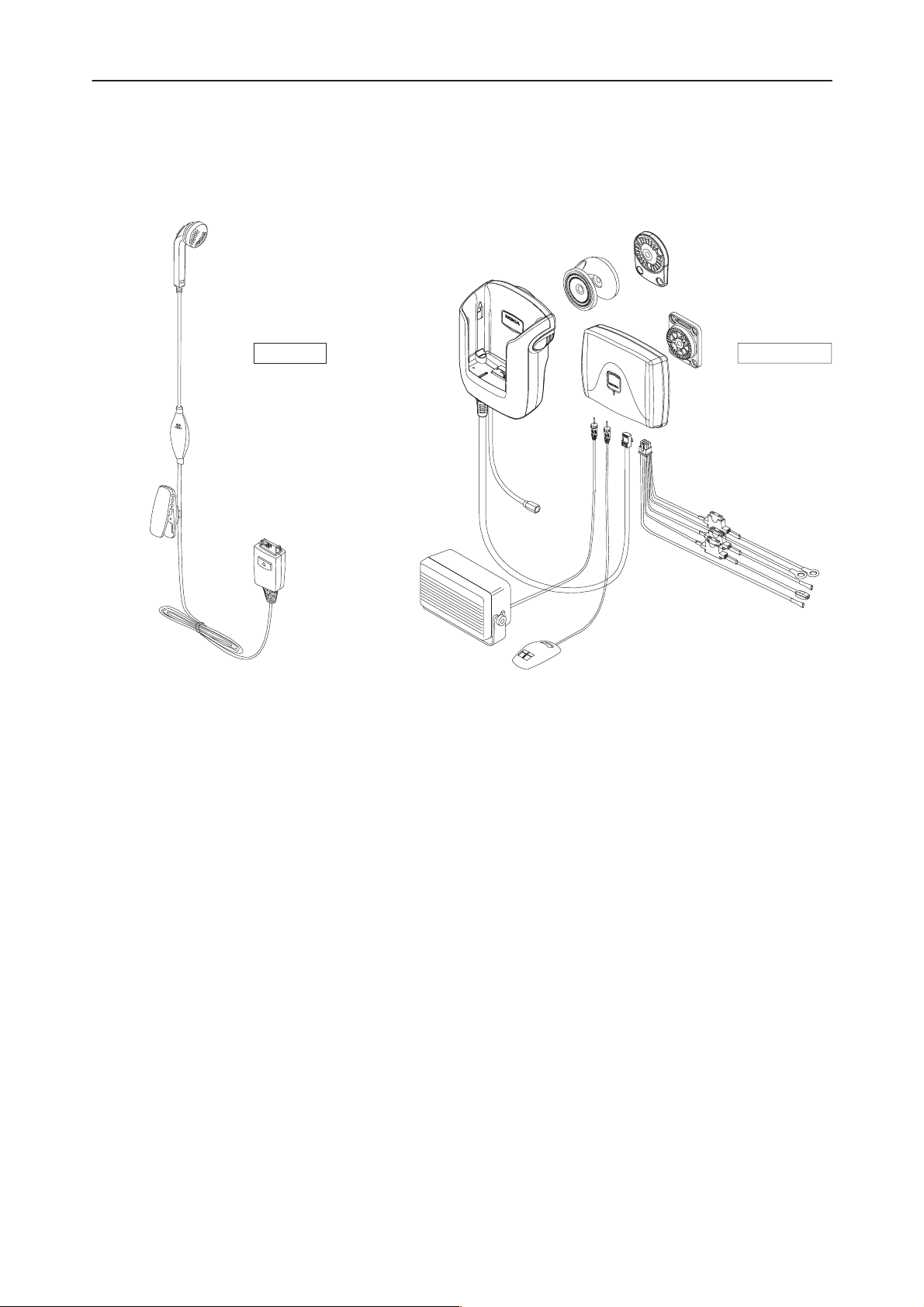
Units and Accessories
Name of unit or accessory Type code Material
code
Battery BLN–3 0670226 1140 mAh, Li–Ion
Performance Travel Charger ACP–9E 0675149 Fore EURO version
Mobile Charger LCH–9 0271056
Advanced Desktop Stand DCH–7 0271365
RS–232 Adapter Cable DLR–2 0730132
Headset HDC–8 0271368
Advanced HF Car Kit CARK–99 0085155
Privacy Handset HSU–1 0270830
Upgrade HF Car Kit CARK–102
Memory Card DTS–4 0271393 Removable memory card MMC
Carrying Case CBR–4 0271410
Notes
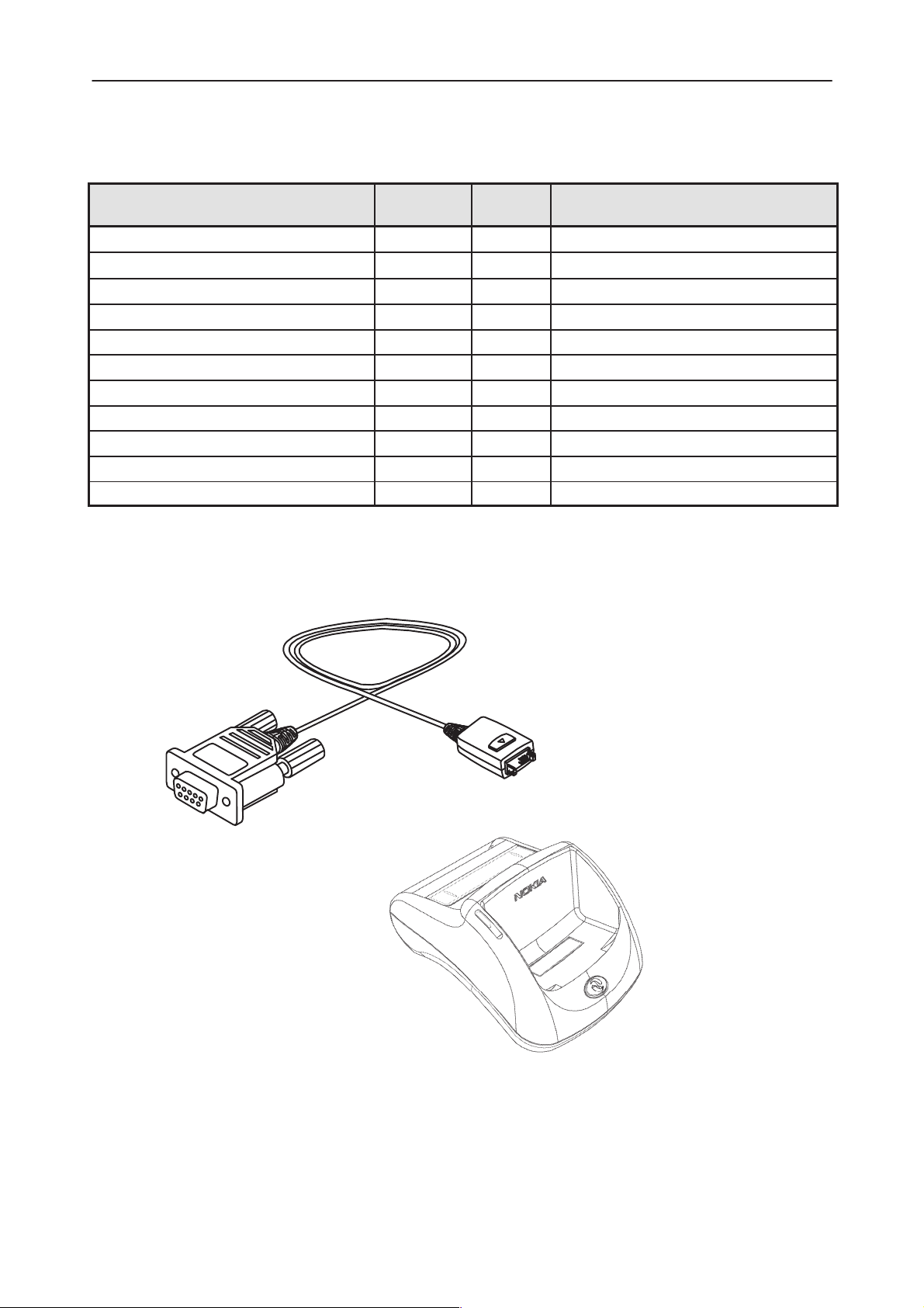
Accessories for PC connection
DLR–2
DCH–7
The desktop stand can charge the transceiver and one BLN–3 battery simultaneously. It also provides connectivity to personal computer. The button in the
front of the deskstand starts synchronization operation if the deskstand is connected to PC with serial cable (DLR–2) and the connectivity software in PC is
activated.
Original 02/99
Page 1–7
Page 8
RAE–2
PAMS
General Information
Audio Accessories
HDC–8 CARK–99
Technical Documentation
Headset differs from DCT3 headset, having a different connector.
The Car kit has a product specific cradle. It is possible to connect DLR–2 PC–
connectivity cable to cradle. Privacy handset (HSU–1) is the same as used
with DCT3 products .
Page 1–8
Original 02/99
Page 9
PAMS
RAE–2
Technical Documentation
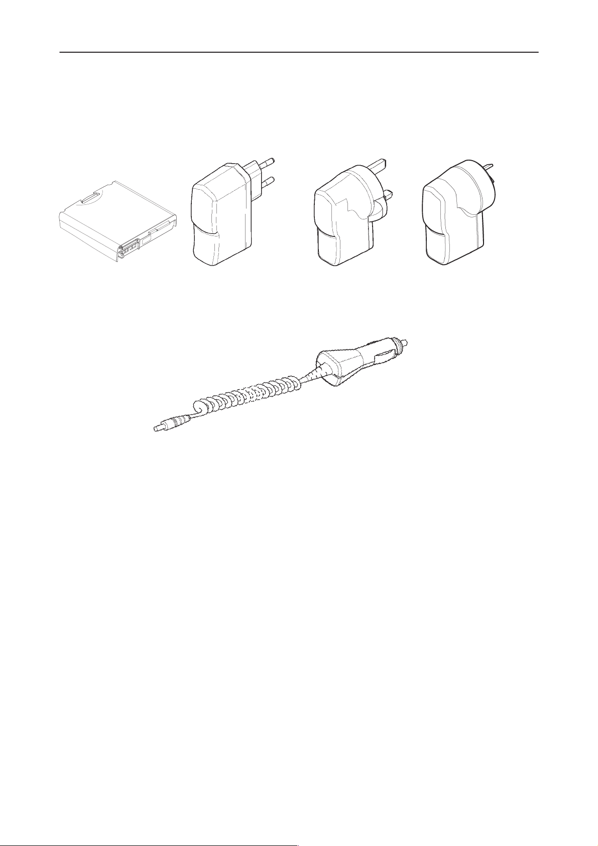
Battery and Chargers
Battery
BLN–3
General Information
European charger
ACP–9E ACP–9X ACP–9A
UK charger Australian charger
Travel charger
Other Accessories
The Memory card DTS–4 provides additional 4MB of user memory into the
product. Memory cards complies to the open MMC specification. In the future
there will be also larger memory capacities available.
LCH–9
Original 02/99
Page 1–9
Page 10
RAE–2
PAMS
General Information
Structure
RAE–2Nx consists of three electrical sub–modules and several mechanical
parts. The structure is basically the same for all the language versions. The
only parts that are unique to each language version are located on the first hierarchy level of the product structure; namely PDA keyboard, Language software
and type label. All other parts and modules are language independent.
Technical Documentation
RAE–2Nx
Lid PDA CMT AssemblyParts PDA
BS1MS1 BS8 MRAE2
UI
BS2
AssemblyParts
MRAE2L
co–label
keyboard
type
label
LanguageSW
List of Modules
Name of module Type code Material
code
MS1 0201224 Lid sub–assembly, contains UI
BS1 BS1 0201096 PDA module, includes CPU and memories
BS8 BS8 0201095 GSM phone module
MRAE2 0261780 Mechanical assembly parts , no language dependent
parts
BS2 BS2 0201097 UI module, includes both LCD’s
MRAE2L 0261786 Assembly parts for lid sub–assembly
Notes
Page 1–10
Original 02/99
Page 11

PAMS
RAE–2
Technical Documentation
General Information
Basic Specifications
Dimensions 56x159x25 mm
Weight 200g (excluding battery)
Battery BLN–3, Li–Ion, 1030mAh, 3.6V, 49,1g
Standby time 5–7 days
Talk time 3–7h
Transceiver GSM, class 4
PDA cpu AMD 486, 33MHz
Fixed user memory 2Mbytes
Fixed application memory 4Mbytes
RAM memory (PDA) 2Mbytes
Original 02/99
Page 1–11
Page 12

RAE–2
PAMS
General Information
Type Labels
Each transceiver with unique mechanics or software has its own type label.
UK English German French
Technical Documentation
Scandinavian Finnish Norwegian
Danish Italian Swedish
APAC1 APAC2 Spanish
Portuguese
Page 1–12
APAC1 and APAC2 are products with UK English user interface with software
settings meant for APAC. Scandinavian product has Scandinavian keyboard but
UK English user interface.
Original 02/99
Page 13

PAMS
RAE–2
Technical Documentation
Keymat Variants
The keymat used depends in the language environment.
General Information
Figure 1. English keymat
Figure 2. French keymat
Original 02/99
Page 1–13
Page 14

RAE–2
PAMS
General Information
Technical Documentation
Figure 3. German keymat
Page 1–14
Figure 4. Italian keymat
Original 02/99
Page 15

PAMS
RAE–2
Technical Documentation
General Information
Figure 5. Spanish keymat
Figure 6. Scandinavian keymat
Original 02/99
Page 1–15
Page 16

RAE–2
PAMS
General Information
Technical Specifications
Modes of Operation
The Communicator has several different operating modes depending on the
activity of CMT and PDA modules. CMT unit can be switched off, idle or call.
PDA can be active, standby, suspended or reset. If the battery voltage is too
low PDA is held in reset–mode.
Electrical Specifications
DC Characteristics
DC–supply for the product is BLN–3 Li–Ion battery. Nominal voltage is 3.6V,
Capacity is 1030mAh i.e. 3708 mWh.
Nominal system voltage for both PDA and CMT is 2.8V.
Technical Documentation
Average Current Consumption
CMT mode
PDA mode Off Idle Call
Active 90 100 240
Standby 60.5 63 185
Suspended 3.2 5.5 165
Backlight power consumption is 60mA. Handsfree consumes about 80mA.
AC Characteristics
Product contains two EL–panels for CMT and PDA display backlighting.
EL Characteristics, PDA and CMT
Parameter Minimum Typical / Nominal Maximum Unit
Frequency 60 70 180 Hz
Peak–to–peak voltage 170 175 180 V
RMS voltage 70 72 75 V
Page 1–16
Original 02/99
Page 17

PAMS
RAE–2
Technical Documentation
General Information
Main RF Characteristics
Item Values
Receive frequency range 935 ... 960 MHz
Transmit frequency range 890 ... 915 MHz
Duplex spacing 45 MHz
Channel spacing 200 kHz
Number of RF channels 124
Power class 4
Number of power levels 15
Transmitter characteristics
Item Values
Type Upconversion, nonlinear, FDMA/TDMA
Intermediate frequency ( phase modulated ) 116 MHz
LO frequency range 1006 ... 1031 MHz
Output power 2 W peak ( 33 dBm )
Power control range min. 5 ... 30 dBm
Maximum phase error ( RMS/peak ) max 5 deg./20 deg. peak
Receiver characteristics
Item Values
Type Linear, FDMA/TDMA
IF frequencies 1st 71 MHz, 2nd 13 MHz
LO frequencies 1st LO 1006 ... 1031 MHz, 2nd LO 58 MHz
Typical 1 dB bandwidth +/– 90 kHz
Sensitivity min. – 102 dBm , S/N >8 dB
Total typical receiver voltage gain ( from antenna
to RX ADC )
Receiver output level ( RF level –95 dBm ) 50 mVpp ( typical balanced signal level of 13 MHz
Typical AGC range –17 ... +40 dB
Accurate AGC control range 57 dB
73 dB
IF in RF BB interface = input level to
RX ADCs )
Typical AGC step in LNA –15 dB
Usable input dynamic range –102 ... –10 dBm
RSSI dynamic range –110 ... –46 dBm
AGC relative accuracy on channel ( accurate
range )
Compensated gain variation in receiving band +/– 1.0 dB
+/– 0.8 dB
Original 02/99
Page 1–17
Page 18

RAE–2
PAMS
General Information
Technical Documentation
Audio characteristics
Minimum Typical /
Nominal
Output freq. range (earpiece) 300 3400 Hz
Output freq. range (HF speak-
er)
Mic. input range. 300 3400 Hz
ringing tone SPL 105 dB at 5 cm
HF speaker SPL 65 dB at 50 cm
Sampling rate 8 kHz
Dynamic range (input) 13 bits
Dynamic range (output) 13 bits
300 3400 Hz
Maximum Unit / Notes
Interconnection Diagram
battery connector
4
Battery
SIM
SIM connector
5
RAE–2Nx
UI, BS2
coax
b2b
CMT, BS8
system connector
3
Charger Accessories PC
hinge–flex
PDA, BS1
4
Memory Card
Card connector
16
Test equipment
Test pads
Page 1–18
Original 02/99
Page 19

PAMS
RAE–2
Technical Documentation
External connections and signals
External Connections:
Battery Connector
Sim Connector
under the card lid
General Information
Test Pads
under the battery
System Connector
IR Window
List of external connectors
Connector Name Code Notes Specifications / Ratings
Battery connector 5469087
System connector 5469091 includes also DC and RF
Memory card connector 5469085 removable memory card
SIM connector 5409089
Test pads PCB test pads for production
and after sales
MMC Connector
under the card lid
SIM and MMC cards cannot be removed until the BLN–3 battery has been removed.
Original 02/99
Page 1–19
Page 20

RAE–2
PAMS
General Information
Technical Documentation
Battery Connector
The Battery connector connects BLN–3 battery to the transceiver. The connector indicates the removal of battery about 5ms before the loss of power because pins BSI and BTEMP are shorter than BVOLT and BGND.
Pin Name Min Typ Max Unit Notes
1 VBATT 3.0 3.6 4.1 V Battery voltage
2 BSI
0 2.85 V Battery size indication
Phone has 180kohm pull up resistor.
SIM Card removal detection
(Threshold is 2.4V@VBB=2.8V)
21.8 22 22.2 kohm BBS–5 Service battery (No cells)
31.35 33 34.65 kohm BLN–3 Li–Ion battery (4.1V)
5 ms The minimum time from BSI contact dis-
engaged its battery contact to VBATT/
GND disengaged its battery contacts
when battery is removed.
3 BTEMP 0 1.4 V Battery temperature indication
Phone has a 100k (+–5%) pull–up resis-
tor,
Battery package has a NTC pull–down re-
sistor:
47k+–5%@+25C , B=4050+–3%
4 GND 0 0 V Battery ground
Page 1–20
Original 02/99
Page 21

PAMS
RAE–2
Technical Documentation
System Connector
The System connector combines the charger, external RF and system functions. External signals can connect to e.g. car kit, headset and PC.
The system connector is not physically compatible with DCT3 connectors except charger.
General Information
PDA SIDE
DC–jack
GND
PDA connections
CHRG_CTRL
VIN
RXTXDTR
XEAR
SGND
Contact Line Symbol CMT Function
1 L_GND Charger ground
DC–jack
L_GND Charger ground
DC–jack
side contact
(DC–plug ring)
DC–jack
VIN Charger input voltage
GND
center pin
DC–jack
CHRG_CTRL Charger control output (from CMT)
side contact
(DC–plug jacket)
2 VIN Charger input voltage
GND
External RF with switch
MBUS
XMIC
Guiding and locking holes
CMT SIDE
PDA SI
3 CHRG_CTRL Charger control output (from CMT)
Original 02/99
Page 1–21
Page 22

RAE–2
PAMS
General Information
CMT FunctionLine SymbolContact
4 SGND Accessory signal ground
5 XEAR Accessory earphone signal output (from CMT)
6 XMIC Accessory microphone signal input (to CMT)
7 MBUS MBUS, bidirectional serial data I/O (DCD in PC use)
8 DCE_RX serial_RX data. (input)
9 DCE_TX serial_TX data. (output)
10 DTR Data Terminal Ready (DTR). No CMT use
11 GND Ground from BS1 module
12,15 GND GND contacts for RF ground
13 RF_OUT RF signal from RF switch to internal antenna
14 RF_IN RF signal from Duplexer to RF switch
Technical Documentation
Page 1–22
Original 02/99
Page 23

PAMS
R
Bidi
l
RAE–2
Technical Documentation
MMC Connector
The MMC connector connects a MMC card to the product. Connector has a
small switch that can detect the opening of the card lid.
1 2 3 4 5 6 7
General Information
Pin I/O Name Function Min Typ Max Unit Description / Note
1 RSV Reserved Reserved for future use
2 I/O MMC_CMD MMC Command / Address /
3 MMC_GND MMC ground VDC
4 I MMC_VSYS MMC Power Supply 2.75 2.85 VDC
5 I MMC_CLK MMC Clock
6 MMC_GND MMC Ground Ground line reserved for
esponse,
rectiona
0 0 0.45 VDC Low, Data to the card
2.3 2.8 2.85 VDC High, Data to the card,
pulled up with 10kohm resistor to MMC_VSYS in
CMT module
0.34 VDC Low, Data from the card
2.1 VDC High, Data from the card,
pulled up with 10kohm resistor to MMC_VSYS in
CMT module
259.3 kHz Frequency
0 0 0.45 VDC Low
2.3 2.8 2.85 VDC High
0.2592 8.294 MHz Frequency
MMC use
Original 02/99
Page 1–23
Page 24

RAE–2
PAMS
General Information
7 I/O MMC_DATA MMC Bidirectional Data
0 0 0.45 VDC Low, Data to the card
2.3 2.8 2.85 VDC High, Data to the card,
0 0 0.34 VDC Low, Data from the card
2.1 VDC High, Data from the card,
8.294 MHz Frequency
Technical Documentation
Description / NoteUnitMaxTypMinFunctionNameI/OPin
pulled up with 10kohm resistor to MMC_VSYS in
CMT module
pulled up with 10kohm resistor to MMC_VSYS in
CMT module
Mechanical Characteristics
Visible product material is ABS+PC except the lens which is clear PMMA. The
bottom part of the device has a magnesium chassis.
Unit Dimensions (mm)
(W x H x D)
Transceiver, RAE–2Nx 56x159x25 202.6
Weight
(g)
Battery, BLN–3 56x58x12 49.1
Page 1–24
Original 02/99
Page 25

PAMS
RAE–2
Technical Documentation
User Interface specifications
The product has tho separate user interfaces (UI): CMT UI on the front cover
and PDA UI which can be accessed by opening the device.
CMT UI conforms to Jack–style defined by NMP. The detailed feature list and
UI specifications can be found in PCMS.
User Interface Features
The RAE–2 has two separate user interfaces (UI): CMT UI on the front cover
and PDA UI which can be accessed by opening the device.
Highlights of the CMT interface are:
General Information
Graphical user
interface, scalable text.
Separate PROFILE–button for selecting CMT profile
Voice recorder
can be activated
from UI.
PDA UI is based on the previous Nokia Communicator product, N9000. The
main difference is that leftmost scroll buttons are replaced by Menu, Zoom and
Backlight buttons.
Original 02/99
Page 1–25
Page 26

RAE–2
PAMS
General Information
Menu
Zoom
Backlight
Menu–button activates an additional pop–up menu window. The contents of the
window depend on the current application. They can be e.g. settings for the
telephone application.
Zoom–button toggles the font size of certain views. The zoomable view depends on the current application. The device has three different zoom levels.
Backlight–button activates the backlight for a pre–set period or until the button
is pressed again. Backlight makes it possible to use the product in low light
conditions.
Technical Documentation
Temperature and Environmental Conditions
Allowed ambient temperature ranges are listed below:
Ambient temperature
(degrees Celcius)
Operating range –10 . . . +55 GSM phase2 requirements ful-
filled.
Extended operating range –20 . . . +70 Device works but not necessarily
fullfill all GSM requirements.
Storage –30 . . . +70 execept battery
Long time storage (sales pack-
age)
0 . . . +30
Allowed ambient relative humidity :
Ambient relative humidity Notes
5 . . . 95 % except battery
The transceiver is not protected against ingress of water. The transceiver may
be instantaneously subjected to dripped or condensed water. Longer term contact with water will cause permanent damage.
Notes
Warnings and Restrictions
See the User Manual.
Page 1–26
Original 02/99
Page 27

PAMS
RAE–2
Technical Documentation
Functional Description
The Communicator comprises two functionally independent units: PDA and
CMT.
The PDA implements the communicator application platform.
The CMT implements the GSM transceiver and basic data functionality, both
transparent and non–transparent data. All UI functionality is combined into one
UI module (BS2) but both PDA and CMT control their respective UI independently.
The Functional units and the implementation differ slightly. Due to mechanical
reasons some components are placed into a different module than they functionally belong. E.g. audio components are placed into BS1 (PDA) module
even if they functionally belong to the CMT.
Block Diagram
General Information
The following diagram describes the functional RAE–2N block diagram.
PDA CMT
FLASH 2MBx16
FLASH 2MBx16
FLASH 2MBx16
DRAM 2MBx16
Earphone
32kHz crystal
PHASER
24
Battery
LiIon 1 140mAh
3.6V
JTAG
Lid buttons
Keyboard
PDA LCD
–backlight
Memory card
2MB – 10MB
SCOTTY
x486 CPU
DRAM controller
KB controller
LCD controller
UART2
PLL
MMC controller
UART1
IrDA 115.2kb/s
Antenna
RF
PA
CRFU
SUMMA
4
7
BB
COBBA
MAD
FLASH 1MBx16
SRAM 128kB
EEPROM 8kB
CCONT
CHAPS
Bottom connector
–charging
–MBUS
–ext. audio
Ext. ant. conn.
Dualaction micHF speaker
CMT LCD
–backlight
CMT keyboard
SIM
PC connectivity
Original 02/99
CMT Accessories
Page 1–27
Page 28

RAE–2
PAMS
General Information
PDA Module
The PDA modules has its own power management chip, the Phaser. The
Phaser regulates the voltages for PDA components. It also controls PDA power–up/down procedure by providing POWERGOOD and RESET signals to
Scotty.
The PDA processor Scotty is an embedded 486 processor manufactured by
AMD. The Scotty contains a set of PC peripherals except a parallel port. It
also has some additional peripherals like LCD controller and MMC host controller which are not standard to PCs. CPU has a 8k cache.
The PDA interfaces the CMT with 115kbps serial bus (FBUS). It also provides
low frequency clock (32kHz) to CMT. PDA also can get information about CMT
state (on/off) and wake up CMT.
CMT Module
The CMT is based on DCT3 engine and it is functionally the same. Sleep clock
(32kHz) is received from PDA side.
Technical Documentation
All the audio components are controlled by CMT (COBBA). It PDA wishes to
play sounds those are first sent to CMT. Keyclicks and some system sounds
are exceptions and are played directly by PDA.
Page 1–28
Original 02/99
Page 29

PAMS
RAE–2
Technical Documentation
Power Distribution
All the digital circuitry modules use 2.8V nominal operating voltage. Power is
drawn from 1140mAh Li–Ion battery. Higher voltages are generated for LCD,
SIM and backlighting.
The diagram below describes the power distribution of the product.
General Information
Audio
The transceiver has two speakers; earpiece for the telephone interface and
handsfree (HF) speaker. Different kind of tones can be played through speakers. HF speaker is driven only by CMT module. The earpiece can be driven
either by the PDA or the CMT. The transceiver has one microphone connected
to the CMT module.
The speakers are used :
Original 02/99
Page 1–29
Page 30

RAE–2
PAMS
General Information
1 HF speaker:
Ringing tones
All PDA tones that can be WAV–type
Talk when HF speaker is enabled
2 Earpiece:
Talk and WAV–sounds when HF disabled
Keyclicks
Fixed PDA tones
Software Specifications of Interfaces
CMT SW is based on HD943. This product program has added internal data
functionality and ECI message interface.
External Devices
External devices can be connected through serial cable (DLR–2) or IR. The
protocols used are:
Technical Documentation
IrOBEX (ir–connectivity),
UltraIR (DCT3 connectivity),
IrDA (PC–connectivity)
IrTranP (camera connectivity).
The PC connectivity uses a specific PCCOM protocol on top of the IrDA or seri-
al connection.
Interfaces Between Transceiver Processors
PDA and CMT processors interface through serial FBUS channel. On top of the
physical FBUS link two separate protocols are used. The Phonet protocol is
used to transport CMT related control information and data–frames. ”RBUS” is
used to transport ECI (External Control Interface) messages between PDA UI
and CMT.
Software–Hardware Interface
CMT sw/hw interface is the same as hd940 is using.
PDA software is running on AMD Elan SC450 processor. Operating frequency
is 33MHz.
Page 1–30
Original 02/99
Page 31

PAMS
RAE–2
Technical Documentation
CMT
GEOS Applications
GEOS Kernel & Services
GEOS
HW–
Drivers
PDA HW Module (BS1)
Spock GS–DOS
Spock GS–BIOS
Testmode
General Information
Manufacturing,
After Sales
and
R&D services
PC
Connectivity
The lowest level of HW/SW interface is handled by the BIOS which provides
some basic services for upper sw layers. E.g. read data from memory card.
Testmode is used by production and After Sales. It provides the interface to
test and program PDA and CMT modules.
DOS layer implements only a subset of DOS functions known from conventional PC. DOS is used mainly in testmode and to launch GEOS.
GEOS is the basic SW platform to all applications that user sees. It however
interfaces directly to some HW resources, like LCD display or serial ports, by
its own HW drivers.
Alignment
Both PDA and CMT modules require alignment. Alignment is done at module
level to modules BS8 and BS1. LCD temperature measurement can be done
only after the assembly of the product.
The following parameters are adjusted in CMT module (BS8): TX power, RSSI,
AFC ,TX I&Q, battery voltage and charging current.
PDA module (BS1) needs alignment of: battery voltage, LCD contrast voltage.
Alignment is software based. Predefined reference point measurements are
stored into EEPROM (CMT) or flash (PDA).
Original 02/99
Page 1–31
Page 32

RAE–2
PAMS
General Information
Flashing
Product requires two separate flash images for executable code: one for the
CMT and one for the PDA system. Language versions are held in separate
files.
CMT flashing uses partly the same equipment as other DCT3 family products.
PDA flashing can be done with JTAG (low level flashing) or WinTesla. WinTesla
flashing is recommended.
Vocabulary
AMD Advanced MIcro Devices
BIOS basic input/output system
CMT cellular mobile telephone
FSTN Film compensated Super Twisted Nematic
HF Hands Free
Technical Documentation
IR infra red
IrDA IR data association
MMC Multi Media Card
PDA personal digital assistant
RX receive
TX transmit
Page 1–32
Original 02/99
 Loading...