

Page 1

PAMS Technical Documentation
RAE–2 Series PDA Phone
Chapter 2
–Transceiver BS8–
Baseband Block
Original 02/99
Copyright 1999 Nokia Mobile Phones. All rights reserved.
Page 2
RAE–2
PAMS
Baseband
Amendment
Number
Technical Documentation
AMENDMENT RECORD SHEET
Date Inserted By Comments
11/98 Original
Page 2– 2
Original 02/99
Page 3

PAMS
RAE–2
Technical Documentation
CONTENTS –Baseband
Introduction 2– 5. . . . . . . . . . . . . . . . . . . . . . . . . . . . . . . . . . . . . . . . . . . .
Technical Summary 2– 5. . . . . . . . . . . . . . . . . . . . . . . . . . . . . . . . . . . . .
Technical Specifications 2– 8. . . . . . . . . . . . . . . . . . . . . . . . . . . . . . . . .
Maximum Ratings 2– 8. . . . . . . . . . . . . . . . . . . . . . . . . . . . . . . . . . . .
DC Characteristics 2– 8. . . . . . . . . . . . . . . . . . . . . . . . . . . . . . . . . . . .
AC Characteristics 2– 8. . . . . . . . . . . . . . . . . . . . . . . . . . . . . . . . . . . .
Connectors 2– 9. . . . . . . . . . . . . . . . . . . . . . . . . . . . . . . . . . . . . . . . . . . .
External Connections from Baseband section of BS8 module 2– 9
Connectors to other modules of the product 2– 9. . . . . . . . . . . . . .
Bottom Connector 2– 9. . . . . . . . . . . . . . . . . . . . . . . . . . . . . . . . . .
Battery Connector 2– 11. . . . . . . . . . . . . . . . . . . . . . . . . . . . . . . . . .
SIM card Connector 2– 12. . . . . . . . . . . . . . . . . . . . . . . . . . . . . . . .
Memory Card Connector 2– 13. . . . . . . . . . . . . . . . . . . . . . . . . . . .
Board to Board Connector 2– 14. . . . . . . . . . . . . . . . . . . . . . . . . . .
RF Coax cable connector 2– 17. . . . . . . . . . . . . . . . . . . . . . . . . . .
Internal Signals and Connections 2– 17. . . . . . . . . . . . . . . . . . . . . . .
Microphone 2– 17. . . . . . . . . . . . . . . . . . . . . . . . . . . . . . . . . . . . . . .
RF– Baseband interface 2– 18. . . . . . . . . . . . . . . . . . . . . . . . . . . .
Baseband
Page No
Functional Descriptions 2– 21. . . . . . . . . . . . . . . . . . . . . . . . . . . . . . . . . .
Power Management 2– 21. . . . . . . . . . . . . . . . . . . . . . . . . . . . . . . . . .
Battery identification 2– 22. . . . . . . . . . . . . . . . . . . . . . . . . . . . . . . .
Battery charging 2– 23. . . . . . . . . . . . . . . . . . . . . . . . . . . . . . . . . . .
Startup charging 2– 23. . . . . . . . . . . . . . . . . . . . . . . . . . . . . . . . . . .
Battery overvoltage protection 2– 24. . . . . . . . . . . . . . . . . . . . . . .
Battery removal during charging 2– 25. . . . . . . . . . . . . . . . . . . . . .
PWM control 2– 25. . . . . . . . . . . . . . . . . . . . . . . . . . . . . . . . . . . . . .
Battery temperature 2– 25. . . . . . . . . . . . . . . . . . . . . . . . . . . . . . . .
Supply voltage regulators 2– 26. . . . . . . . . . . . . . . . . . . . . . . . . . .
MAD core regulator 2– 27. . . . . . . . . . . . . . . . . . . . . . . . . . . . . . . . .
Switched mode supply VSIM 2– 28. . . . . . . . . . . . . . . . . . . . . . . .
Power up 2– 28. . . . . . . . . . . . . . . . . . . . . . . . . . . . . . . . . . . . . . . . .
Power up with power switch (PWRKEYx) 2– 28. . . . . . . . . . .
Power up with a charger 2– 29. . . . . . . . . . . . . . . . . . . . . . . . . .
Service Request State (SRS) 2– 30. . . . . . . . . . . . . . . . . . . . . .
Active Mode 2– 31. . . . . . . . . . . . . . . . . . . . . . . . . . . . . . . . . . . . . . .
Sleep Mode 2– 32. . . . . . . . . . . . . . . . . . . . . . . . . . . . . . . . . . . . . . .
Charging 2– 32. . . . . . . . . . . . . . . . . . . . . . . . . . . . . . . . . . . . . . . . . .
Power Off 2– 32. . . . . . . . . . . . . . . . . . . . . . . . . . . . . . . . . . . . . . . . .
Watchdog 2– 33. . . . . . . . . . . . . . . . . . . . . . . . . . . . . . . . . . . . . . . . .
Original 02/99
Page 2– 3
Page 4

RAE–2
PAMS
Baseband
Audio control 2– 33. . . . . . . . . . . . . . . . . . . . . . . . . . . . . . . . . . . . . . . . .
PDA Tones 2– 34. . . . . . . . . . . . . . . . . . . . . . . . . . . . . . . . . . . . . . . .
CMT Alert Signal Generation 2– 34. . . . . . . . . . . . . . . . . . . . . . . .
External audio connections 2– 34. . . . . . . . . . . . . . . . . . . . . . . . . .
Analog audio accessory detection 2– 36. . . . . . . . . . . . . . . . . . . .
Headset detection 2– 36. . . . . . . . . . . . . . . . . . . . . . . . . . . . . . . . . .
Headset switch detection 2– 36. . . . . . . . . . . . . . . . . . . . . . . . . . . .
Internal audio connections 2– 37. . . . . . . . . . . . . . . . . . . . . . . . . . .
4–wire PCM serial interface 2– 37. . . . . . . . . . . . . . . . . . . . . . . . .
Digital control 2– 38. . . . . . . . . . . . . . . . . . . . . . . . . . . . . . . . . . . . . . . .
MAD2 2– 38. . . . . . . . . . . . . . . . . . . . . . . . . . . . . . . . . . . . . . . . . . . .
MAD2 memory configuration 2– 40. . . . . . . . . . . . . . . . . . . . . .
MCU Memory Map 2– 41. . . . . . . . . . . . . . . . . . . . . . . . . . . . . . .
Memories 2– 41. . . . . . . . . . . . . . . . . . . . . . . . . . . . . . . . . . . . . . . . .
Program Memory 2– 41. . . . . . . . . . . . . . . . . . . . . . . . . . . . . . . .
SRAM Memory 2– 42. . . . . . . . . . . . . . . . . . . . . . . . . . . . . . . . . .
EEPROM Memory 2– 42. . . . . . . . . . . . . . . . . . . . . . . . . . . . . . .
Flash Programming 2– 43. . . . . . . . . . . . . . . . . . . . . . . . . . . . . . . .
RAE–2 Flashing connections 2– 43. . . . . . . . . . . . . . . . . . . . . .
Flashing methods 2– 43. . . . . . . . . . . . . . . . . . . . . . . . . . . . . . . .
Flashing procedure 2– 44. . . . . . . . . . . . . . . . . . . . . . . . . . . . . .
Security 2– 45. . . . . . . . . . . . . . . . . . . . . . . . . . . . . . . . . . . . . . . .
COBBA–GJ ASIC 2– 45. . . . . . . . . . . . . . . . . . . . . . . . . . . . . . . . . .
Technical Documentation
Page 2– 4
Original 02/99
Page 5
PAMS
RAE–2
Technical Documentation
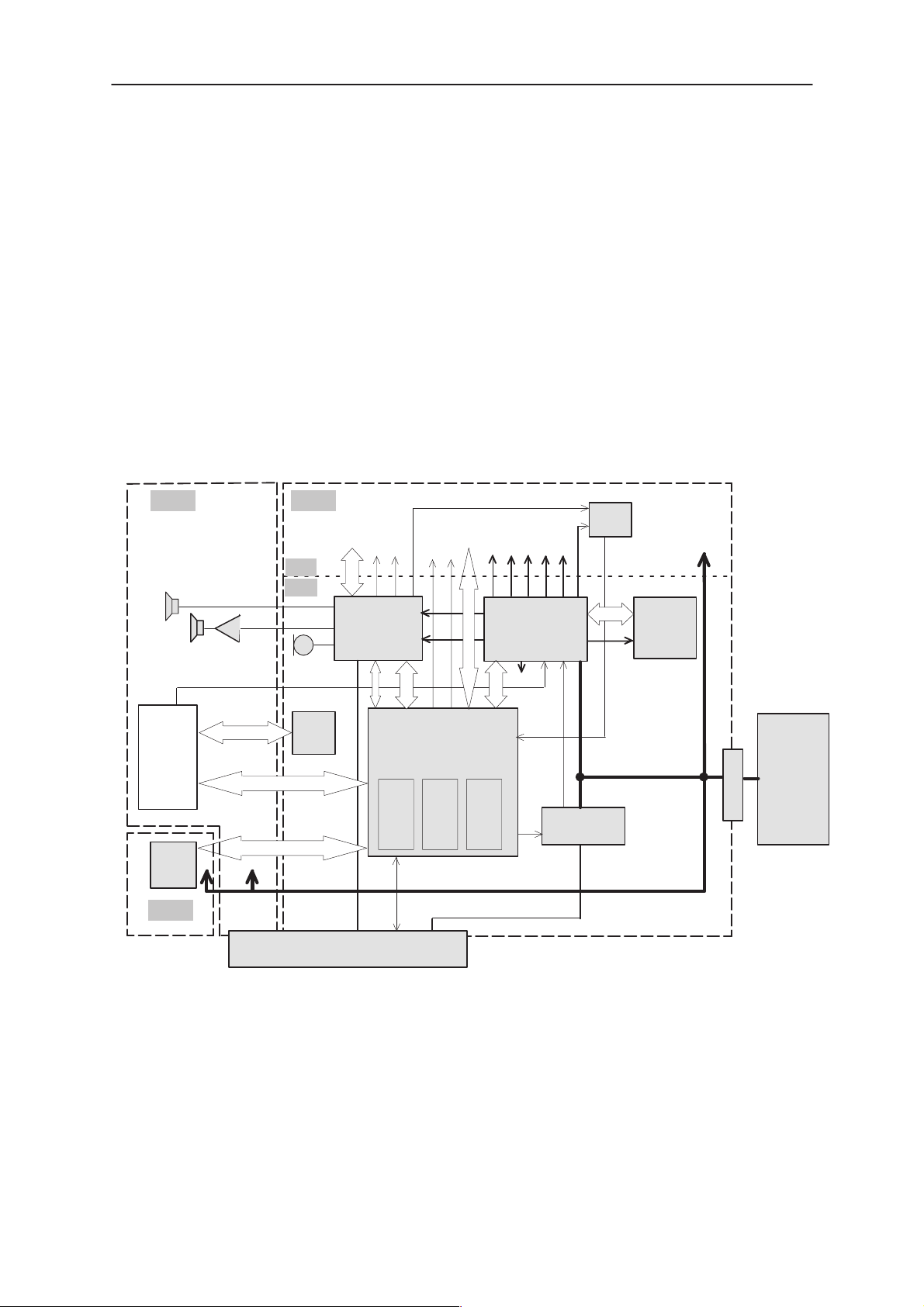
Introduction
This document contains the specification to the Baseband section of the
BS8 module. The BS8 module carries out almost all CMT functions of
RAE–2. BS8 can be divided into two functional sections; BaseBand (BB)
and RF. Some of CMT baseband circuits are implemented to both BS1
and BS2 modules.
The Baseband module BS8 comprises four ASICs (CHAPS, CCONT,
COBBA–GJ and MAD2) that perform the baseband functions of the mod-
ule.
BS1
earphone
HF
BS8
RF
BB
MIC
TX/RX
TXC RXC
COBBA
TXPa
Synthesizer
control
LNA
RF SUPPLIES
VREF
CCONT
VCOBBA
VBB
AFC
VCOPWR
32kHz
Baseband
VCTCXO
13MHz
PA SUPPLY
SIMCONN
VSIM
MMC IF
SCOTTY
CMT
UI
BS2
MMC
CONN
CMT–PDA IF
CMTUI IF
Ext. audio
IF
BOTTOM CONNECTOR
Figure 1. BS8 BaseBand block in RAE–2 product
Technical Summary
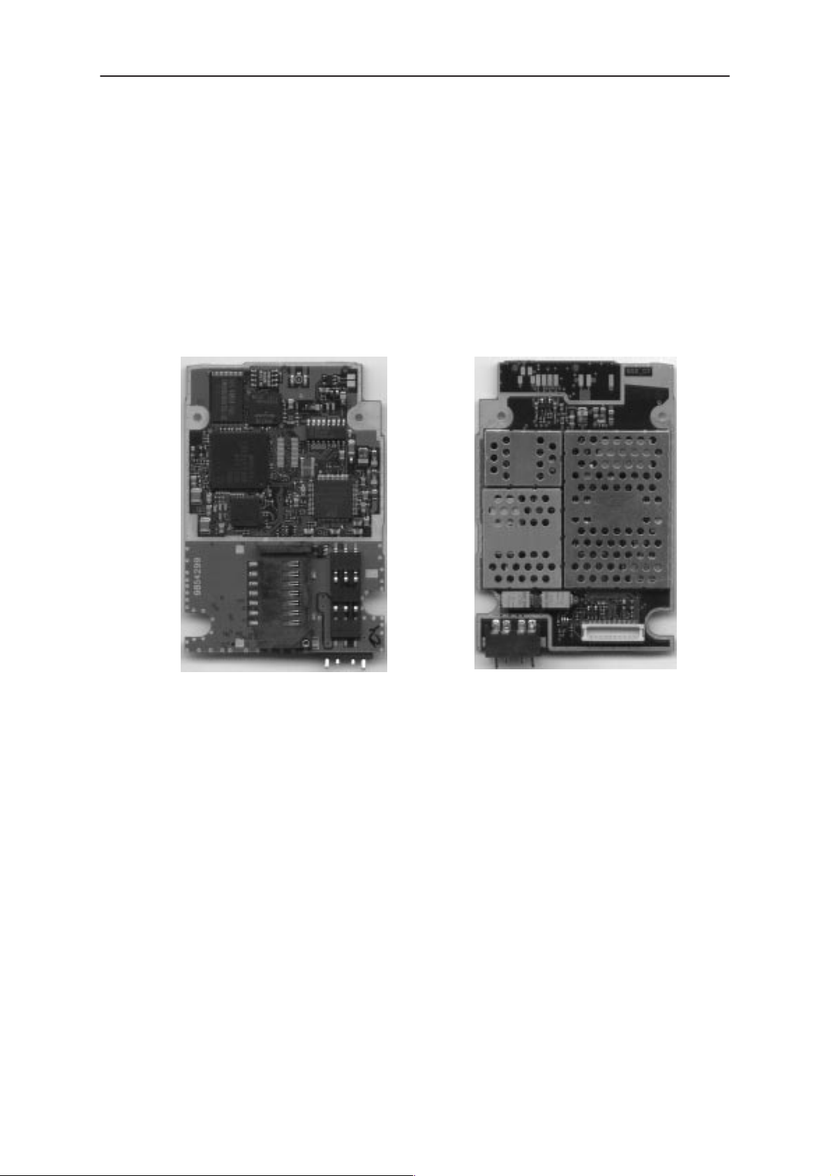
The BS8 module is implemented on a single double side 8–layer printed
circuit board. The main part of the baseband area is located on the bot-
tom side of the PCB and only some components (bottom connector, bat-
tery connector and some filter components) are placed on the upper side
(RF side). Component height space on the baseband is 2.0mm.
Flash
512k
MAD
+
Memories
MAD
Sram
256k
MBUS
Eeprom
8k
VCHARG
CHAPS
LIM
Charger IF
VBATT
BATTERY
BATT.CONN
Original 02/99
Page 2– 5
Page 6
RAE–2
PAMS
Baseband
Technical Documentation
The baseband is running from a 2.8V power rail, which is supplied by the
power controlling ASIC. In the CCONT ASIC there are 6 individually con-
trolled regulator outputs for RF–section and two outputs for the base-
band. In addition there is one +5V power supply output (V5V) for flash
programming voltage and for other purposes where a higher voltage is
needed. The CCONT contains also a SIM interface, which supports both
3V and 5V SIM–cards.
BaseBand Side RF Side
Figure 2. BS8 Module
The interface between the baseband and the RF section is handled by
the specific ASIC COBBA. The COBBA provides:
– A/D and D/A conversion of the in–phase and quadrature receive and
transmit signal paths
– A/D and D/A conversions of received and transmitted audio signals to
and from the UI section.
The COBBA supplies the analog TXC and AFC signals to the RF section
according to the MAD DSP digital control and converts the analog AGC
into digital signal for the DSP. The data transmission between the COB-
BA and the MAD is implemented using a parallel connection for high
speed signalling and a serial connection for PCM coded audio signals.
Digital speech processing is handled by the MAD asic.
The COBBA is a dual voltage circuit, the digital parts are running from the
baseband supply VBB and the analog parts are running from the analog
supply VCOBBA.
Page 2– 6
Original 02/99
Page 7
PAMS
RAE–2
Technical Documentation
The COBBA supports three microphone inputs and two earphone out-
puts. The inputs can be taken from an internal microphone, a headset mi-
crophone or from an external microphone signal source.
The output for the internal earphone is a dual ended type output capable
of driving a dynamic type speaker. Input and output signal source selec-
tion and gain control are performed inside the COBBA according to con-
trol messages from the MAD. Call alerts, keypad tones, DTMF, and other
audio tones are generated and encoded by the MAD and transmitted to
the COBBA for decoding.
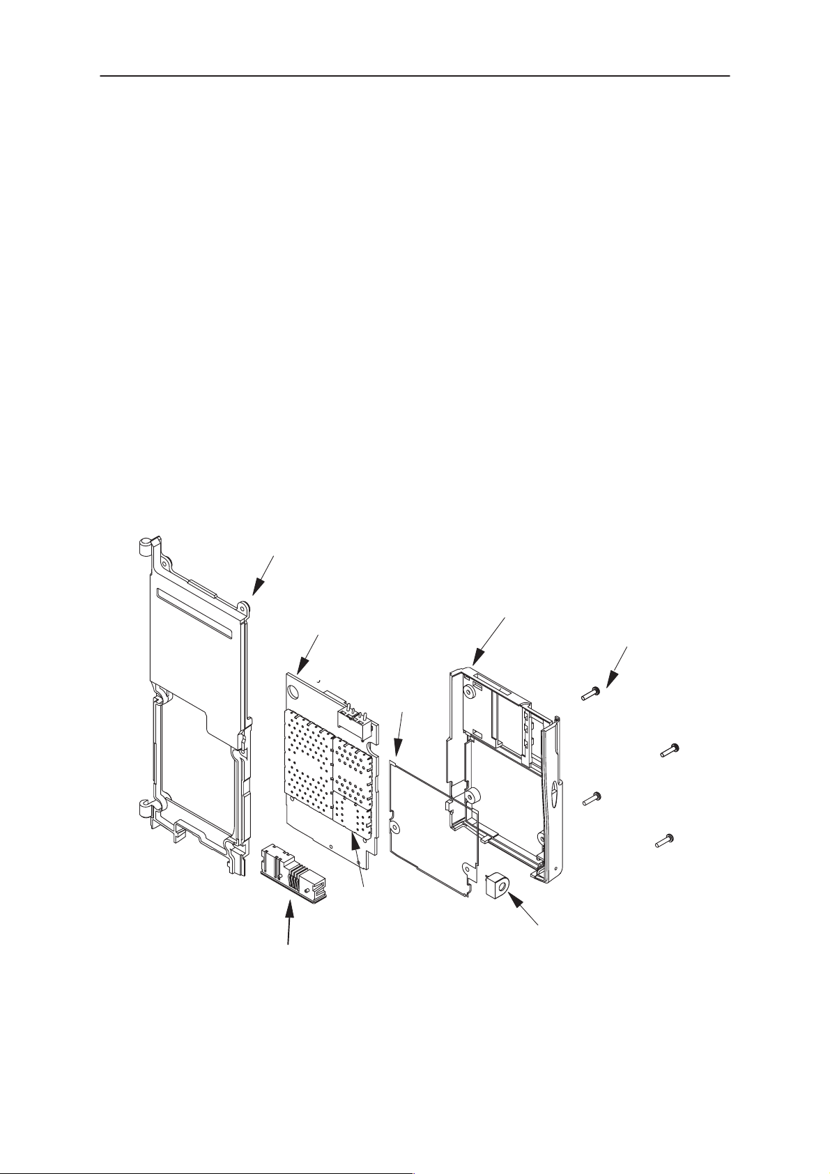
EMC shielding (figure below) is implemented on the BB side using a me-
tallized plastic B–cover and conductive gasket between the B–cover and
the PCB. On the RF side the engine is shielded with a conductive frame
which makes a contact to a ground ring of the CMT board and a ground
plane of the PDA board. There is a conductive gasket between the frame
and the PCB for ensuring proper shielding. In addition he RF area has
three metal cans for RF shielding. Heat generated by the circuitry is con-
ducted out mainly via the PCB ground planes.
Baseband
Conductive frame +gasket
BS8 module
Metal
gasket
Metal cans
Bottom connector
Metallized B–cover
4 srews for fastening
B–cover to frame
Microphone
Original 02/99
Page 2– 7
Page 8
RAE–2
PAMS
Baseband
Technical Documentation
Technical Specifications
Maximum Ratings
Parameter Rating
Battery voltage, idle mode –0.3 ... 4.1V without charger
Charger input voltage –5.0 ... 16V
Operating temperature range –25C to +70 C
Storage temperature range –40C to +85 C
DC Characteristics
Supply voltages
Line Symbol Minimum Typical /
Nominal
Supply battery voltage 3.0 3.6 4.1 V
Battery powerup voltage (HW) 2.9 3.0 3.1 V
Battery cut off voltage (HW) 2.7 2.8 2.9 V
Regulated baseband supply voltage 2.7 2.8 2.85 V
Regulated baseband supply current 3 50 125 mA
Regulated VCORE supply voltage 1.3 – 2.65 V (changeable)
Regulated VCORE supply current 50 mA
COBBA analog supply voltage 2.7 2.8 2.85 V
COBBA analog supply current 5 20 100 mA
Regulated 5V supply voltage 4.8 5.0 5.2 V
Regulated 5V supply current 0 1 30 mA
Regulated 5V SIM supply voltage 4.8 5.0 5.2 V
Regulated 5V SIM supply current 3 10 30 mA
Regulated 3V SIM supply voltage 2.8 3.0 3.2 V
Regulated 3V SIM supply current 1 6 30 mA
Voltage reference 1.4775 1.5 1.5225 V
Maximum Unit / Notes
Note: The RF voltages are described later
AC Characteristics
Line symbol Minimum Typical /
32kHz 32768 Hz, Sleep clock
RFIClk 13 MHz, System clock
PCMClk 8 kHz, PCM clock
SIMClk 3.25 MHz, SIM Clock
Page 2– 8
Table 1. AC Specifications
Maximum Unit / Notes
Nominal
Original 02/99
Page 9
PAMS
RAE–2
Technical Documentation
Baseband
Connectors
External Connections from Baseband section of BS8 module
This section describes the external electrical connections and interface
levels on the baseband section of the BS8 module. The electrical inter-
face specifications are collected into tables that cover a connector or a
defined interface each.
Connectors to other modules of the product
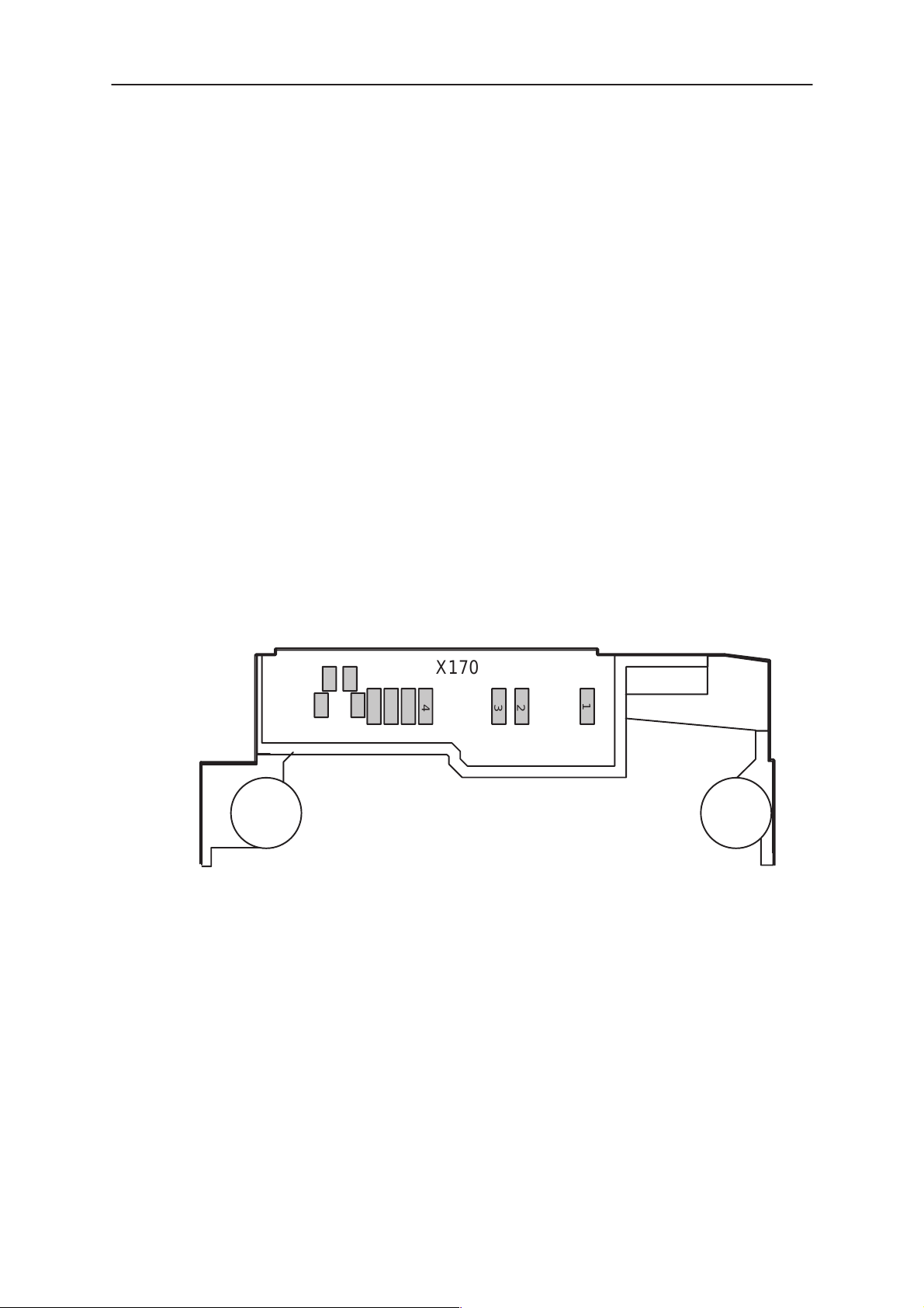
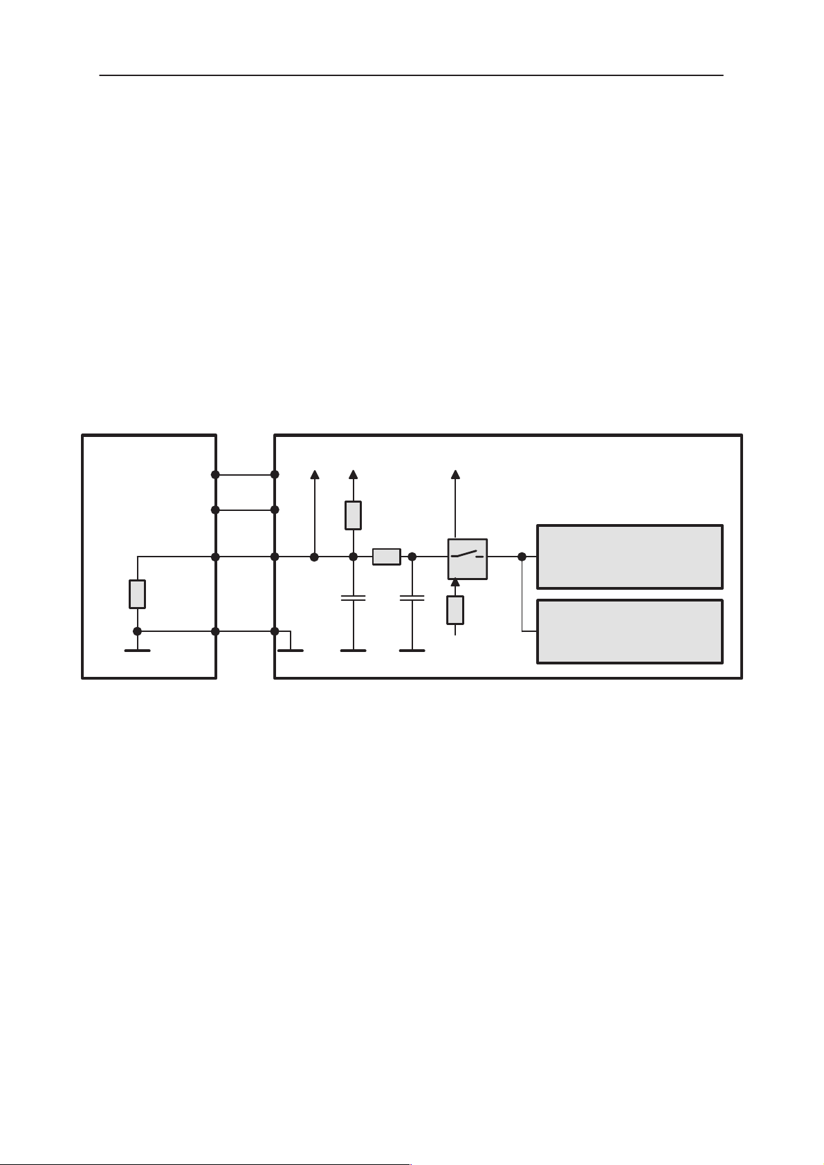
Bottom Connector
The bottom connector has spring type of connections. In BS8 module
there are contact pads for the spring connections.
10
9
11
Figure 3. Bottom connector pads in BS8 module
6
7
8
X170
5
4
2
3
1
The electrical specifications in the next table show the bottom connector
signals and levels on the baseband. The system connector is used to
connect the transceiver to accessories. The table gives the idle voltage
produced by the acceptable chargers at the DC connector input. The ab-
solute maximum input voltage is 30 V due to the transient suppressor that
is protecting the charger input.
Original 02/99
Page 2– 9
Page 10
RAE–2
CTRL
Baud rate 9600 Bit/s
PAMS
Baseband
Technical Documentation
Table 2. Baseband signals of the bottom connector (X170)
Pin Name Min Typ Max Unit Notes
1 L_GND 0 0 V Supply ground
2 VIN
3 CHRG_
4 SGND
7.25
3.25
320
7.1
3.25
720
0 0.5 V Charger control PWM low
2.0 2.85 V Charger control PWM high
1 99 % PWM duty cycle
7.6
3.6
370
8.4
3.6
800
32 Hz PWM frequency for a ACP–9
47 Ω Output AC impedance (ref. GND)
10 µF Series output capacitance
380 Ω Resistance to phone ground
7.95
16.9
3.95
420
9.3
3.95
850
V
V
V
mA
V
V
mA
Unloaded ACP–7 Charger (5kohms load)
Peak charger output voltage (5kohms load)
Loaded charger output voltage (10ohms load)
Supply current
Unloaded ACP–9 Charger
Loaded charger output voltage (10ohms load)
Supply current
5 XEAR
HEAR 28 626 mV Earphone signal (HF– HFCM)
6 XMIC
HMIC 0 3.2 29.3 mV Microphone signal
47 Ω Output AC impedance (ref. GND)
10 µF Series output capacitance
16 300 Ω Load AC impedance to SGND (Headset)
4.7 10 kΩ Load AC impedance to SGND (Accessory)
1.0 Vpp Maximum output level (no load)
22 626 mV Output signal level
10 kΩ Load DC resistance to SGND (Accessory)
16 1500 Ω Load DC resistance to SGND (Headset)
2.8 V DC voltage (47k pull–up to VBB)
Connected to COBBA HF output
2.0 2.2 kΩ Input AC impedance
1 Vpp Maximum signal level
1.47 1.55 V Mute (output DC level)
2.5 2.85 V Unmute (output DC level)
100 600 µA Bias current
58 490 mV Maximum signal level
Connected to COBBA MIC3P input
7 MBUS 0 logic low 0.5 V Serial bidirectional control bus.
2.1 logic high 2.85
12,1
5
13 RF_OUT 5 (TX levels) 33 dBm RF signal from RF switch to internal antenna
14 RF_IN 5 (TX levels) 33 dBm RF signal from PA to RF switch.
GND 0 0 V RF ground
Page 2– 10
Phone has a 4k7 pullup resistor
Original 02/99
Page 11
PAMS
RAE–2
Technical Documentation
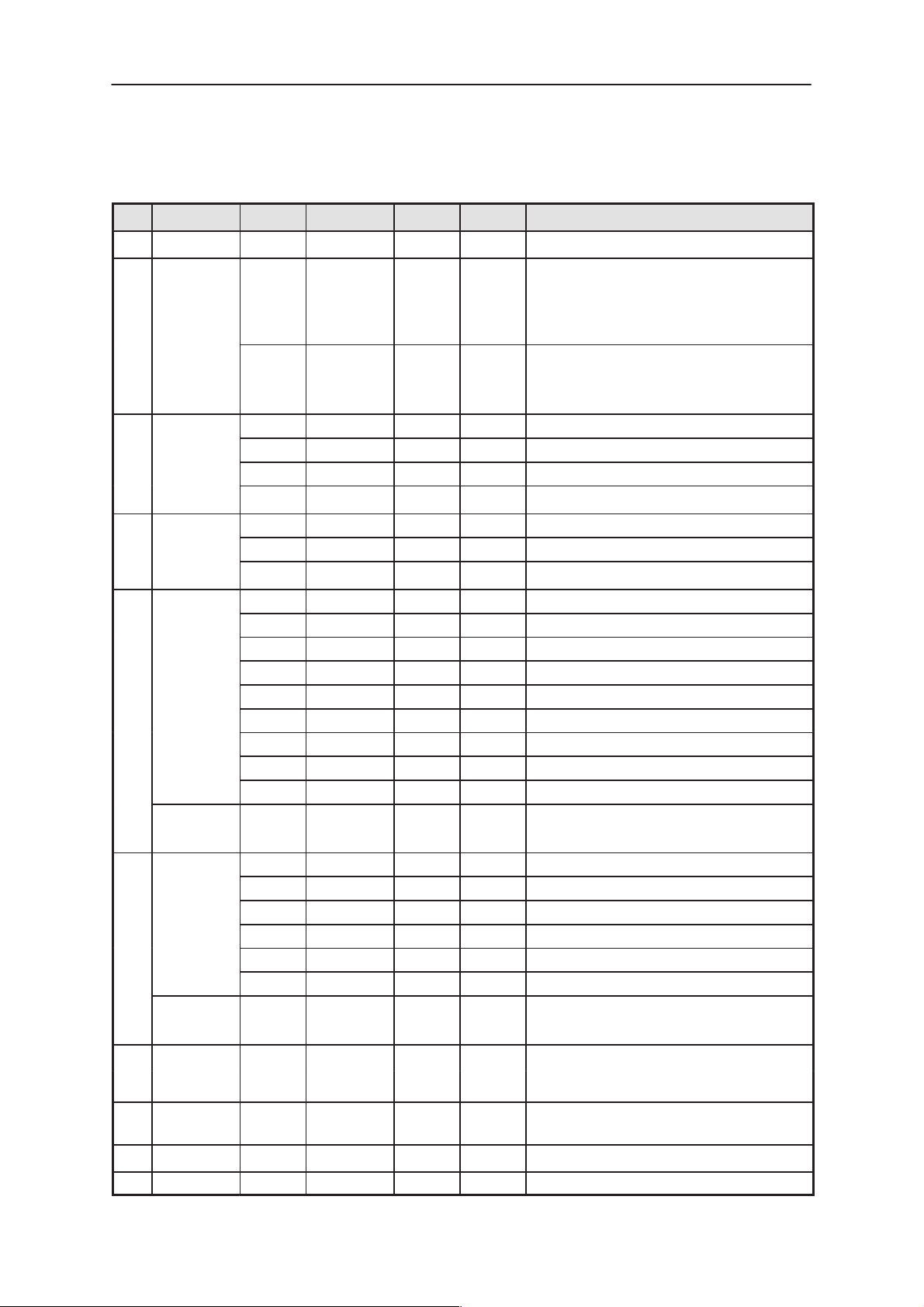
The bottom connector has mounting holes for a fastening to a shielding
frame located between the PDA and CMT modules. The bottom connector has spring type connections to the CMT and the PDA module.
The bottom connector includes the following parts:
– DC connector for external plug–in charger and a desktop charger
– System connector for accessories.
– Connector for external RF signal. This connector is equipped with
throw–over–switch. This is needed to change the RF signal path between external and internal antenna depending whether the ext antenna cable is connected or not.
PDA connections
RXTXDTR
GND
Baseband
PDA SIDE
External RF with switch
MBUS
XMIC
DC–jack
GND
Battery Connector
The electrical specifications for the battery connector are listed in the
next table. The BSI contact of the battery connector is also used to detect
when the battery is removed suddenly.
This information is needed for driving the SIM card safely down before
supply voltage is lost. The BSI contact in the battery connector has
0.5mm shorter working length than
the supply power contacts to give
enough time for the SIM shut down.
CHRG_CTRL
VIN
Figure 4. Bottom Connector
XEAR
SGND
Guiding and locking holes
GND
CMT SIDE
X160
BSI BTEMP
VBATT
Original 02/99
Figure 5. Battery Connector
Page 2– 11
Page 12
RAE–2
PAMS
Baseband
Technical Documentation
Table 3. Battery Connector Electrical Specifications (X160)
Pin Name Min Typ Max Unit Notes
1 VBATT 3.0 3.6 4.1 V Battery voltage
2 BSI
3 BTEMP
4 GND 0 0 V Battery ground
0 2.85 V Battery size indication
CMT has 180kohm pull up resistor.
SIM Card removal detection
(Threshold is 2.4V@VBB=2.8V)
17.1 18 18.9 kohm Field Test Battery (4.1V)
21.8 22 22.2 kohm BBS–5 Service battery (No cells)
31.35 33 34.65 kohm BLN–3 Li–ion battery (4.1V)
5 ms The minimum time from BSI contact disengaged its bat-
tery contact to VBATT/GND disengaged its battery con-
tacts when battery is removed.
0 1.4 V Battery temperature indication
CMT has a 100k (+–5%) pullup resistor,
Battery package has a NTC pulldown resistor:
47k+–5%@+25C , B=4050+–3%
0 1 kohm Local mode initialization (in production)
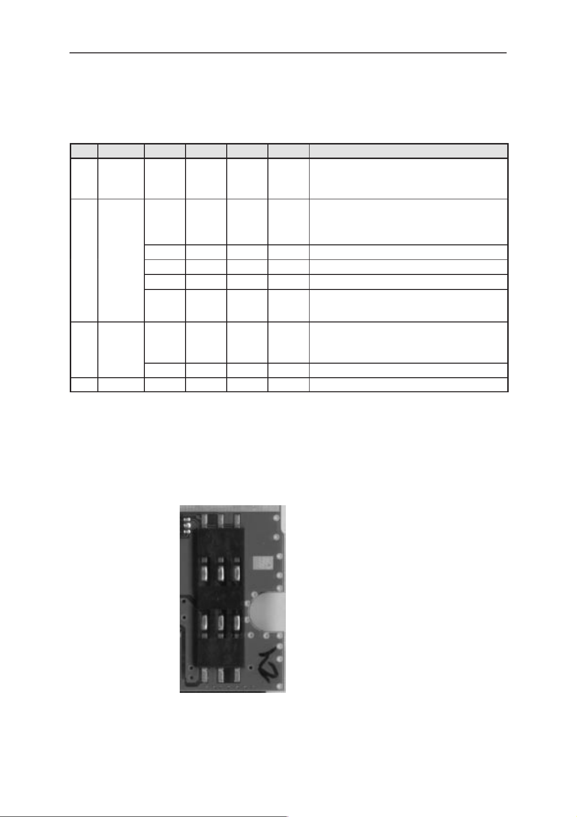
SIM card Connector
The SIM card connector is located on the baseband side of the BS8 module. The contacts of the SIM card connector are protected against electric discharge with ESD protection components.
VSIM
X150
GND
SIMRST
VSIM
SIMDATA SIMCLK
Page 2– 12
Figure 6. SIM Card Connector
Original 02/99
Page 13
PAMS
RAE–2
Technical Documentation
Table 4. SIM Connector Electrical Specifications (X150)
Pin Name Parameter Min Typ Max Unit Notes
4 GND GND 0 0 V Ground
3, 5 VSIM 5V SIM Card
3V SIM Card
6 DATA 5V Vin/Vout
3V Vin/V out
2 SIMRST 5V SIM Card
3V SIM Card
1 SIMCLK Frequency
Trise/Tfall
4.8
2.8
4.0
2.8
4.0
2.8
5.0
3.0
”1”
0
0
”0”
”1”
”0”
”1”
”1”
3.25
5.2
3.2
VSIM
0.5
VSIM
0.5
VSIM
VSIM
25
V Supply voltage
V SIM data
Trise/Tfall max 1us
V SIM reset
MHz
ns
SIM clock
VSIM supply voltages are specified to meet type approval requirements
regardless the tolerances in components.
Baseband
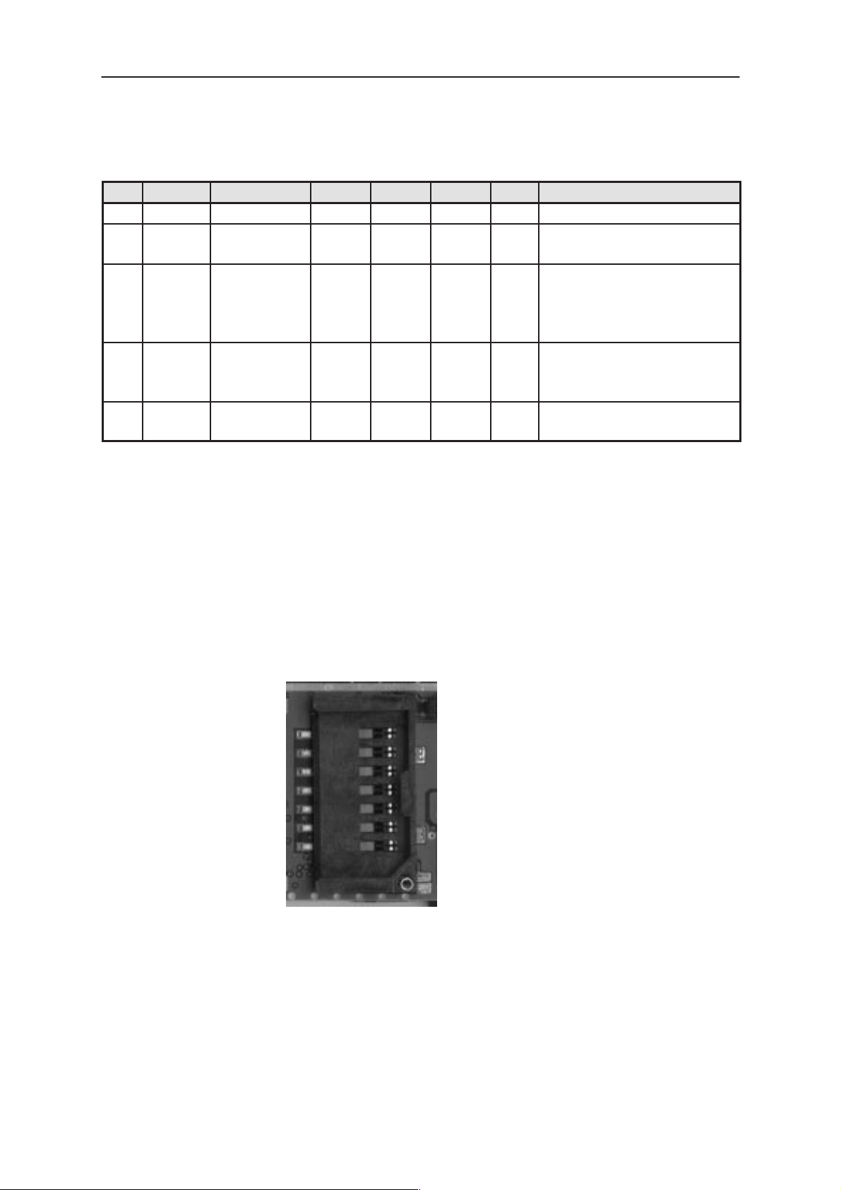
Memory Card Connector
The Memory card connector locates on BS8 module. Memory card is a
changeable Flash or ROM memory with variable memory size. The PDA
CPU can access with Memory card via synchronous serial interface.
Memory card signals are routed from BS1 module to BS8 module through
board to board connector.
MMC_DATA
MMC_GND
MMC_CLK
MMC_VSYS
MMC_GND
MMC_CMD
Figure 7. Memory Card Connector
X191
NC
The signals of the MMC connector are specified in the board to board
connector table.
Original 02/99
Page 2– 13
Page 14
RAE–2
3,4
PAMS
Baseband
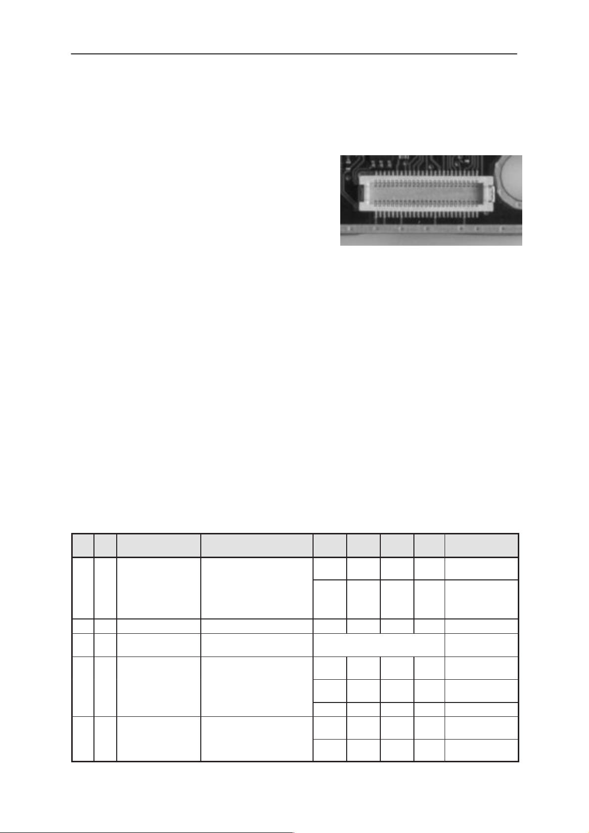
Board to Board Connector
All interfaces (except RF antenna
signal) from the BS8 module to the
other RAE–2 modules are routed
over a 50–pins board to board connector. The interfaces can be divided into several groups; CMT–UI,
CMT–HF audio, CMT–PDA, MMC–
PDA and supply lines for the BS1
and the BS2 modules.
The CMT keyboard with keyboard illumination parts and the CMT display
module with display illumination parts are implemented on a separate UI
module (BS2), which contains also the PDA user interface and an antenna matching circuit. The baseband signals to the UI are routed over an
board to board connector to the BS1 module and from the BS1 module
through the hinge flex to the BS2 module.
Technical Documentation
pin 25pin 1
X190
pin 26pin 50
Figure 8. BoBo Connector
The Handsfree speaker and earpiece are included in the audio holder.
Because the audio holder and the HF amplifier are located on the PDA
module, several signals through the board to board connector are needed for carrying audios from the CMT to the PDA.
There are data signals for data transmission between the CMT and the
PDA modules. Some I/O signals are needed for carrying logic state information between modules.
Signal definition and the most important specifications of signals are listed
in the next table.
Table 5. Board to Board Connector (X190)
Pin I/O Name Function Min Typ Max Unit Description /
1,2,
,
5
6 O XEAR Audio Output for Handsfree 500 mVpp
7 GND Global Ground Reference for oth-
8 O BATTDET Battery Position Information
9 O HFENA Internal Handsfree Amplifier
VBATT Battery Positive
Control
3.0 3.6 4.1 VDC Unregulated Bat-
1.5 1000 mA Current to BS1
0.23 0.26 0.28 VDC Field T est battery
0.28 0.30 0.33 VDC Service battery
0.39 0.43 0.48 VDC BLN–3 battery
0 0.5 VDC Low, HF amplifier
2.1 2.85 VDC High, HF amplifier
Note
tery Voltage
and BS2 module
(max=peak current)
er signals
(only R&D use)
(BBS–5)
disabled
enabled
Page 2– 14
Original 02/99
Page 15

PAMS
between EARP
RAE–2
Technical Documentation
Table 5. Board to Board Connector (X190) (continued)
10 O EARP Earpiece Positive
11 O EARN Earpiece Negative
12 GND Global Ground
13 I PWRONx PDA start CMT to Service Re-
quest State (SRS)
14 I 32kHz Sleep clock to CMT
15 GND Global Ground
16 O VBB CMT regulated system volt-
age
17 I PWRKEYx CMT Power On/Off Switch
18 O CMT_BL_ON CMT UI Backlight On
19 I ROW3 CMT Keys Row 3
20 I ROW2 CMT Keys Row 2
21 I ROW1 CMT Keys Row 1
22 I ROW0 CMT Keys Row 0
23 GND Global Ground
24 O COL4 CMT Keys Column 4
25 O COL3 CMT Keys Column 3
26 O COL2 CMT Keys Column 2
27 O COL1 CMT Keys Column 1
28 O COL0 CMT Keys Column 0
29 GND Global Ground
Baseband
Description /
UnitMaxTypMinFunctionNameI/OPin
Note
50 223 mVpp Differential voltage
and EARN nodes
0 0.45 VDC Active state, min.
2.3 2.8 2.85 VDC Inactive state
0 0.45 VDC Pulse low level
2.3 2.8 2.85 VDC Pulse high level
12 mA Maximum current
32768 Hz Pulse frequency
20 50 80 % Duty cycle (CMT
1 % Jitter (CMT re-
2.7 2.8 2.85 VDC Regulated CMT
1 mA Maximum current
0 0.5 Low, active state
2.7 2.85 VDC High, inactive state
0 0.5 VDC Low, backlight off
2.1 2.8 2.85 VDC High, backlight on
0 0.2 VDC Low
2.5 2.8 2.85 VDC High
0 0.2 VDC Low
2.5 2.8 2.85 VDC High
0 0.2 VDC Low
2.5 2.8 2.85 VDC High
0 0.2 VDC Low
2.5 2.8 2.85 VDC High
0 0.5 VDC Low
2.1 2.85 VDC High
0 0.5 VDC Low
2.1 2.85 VDC High
0 0.5 VDC Low
2.1 2.85 VDC High
0 0.5 VDC Low
2.1 2.85 VDC High
0 0.5 VDC Low
2.1 2.85 VDC High
64ms
from PDA
requirements)
quirements)
baseband voltage
Original 02/99
Page 2– 15
Page 16

RAE–2
Sel
Clock
D
USE!
PAMS
Baseband
Technical Documentation
Table 5. Board to Board Connector (X190) (continued)
Description /
UnitMaxTypMinFunctionNameI/OPin
Note
30 O LCDCD CMT LCD Command / Data
ect
31 O LCDRSTx CMT LCD Reset
32 O LCDCSx CMT LCD Chip Select
33 GND Global Ground
34 O GENSCLK CMT LCD and CCONT Serial
35 O GENSDIO CMT LCD and CCONT Serial
ata
36 GND Global Ground
37 I FBUS_RXD Fast Serial Data to CMT
38 0 FBUS_TXD Fast Serial Data to PDA
39 GND Global Ground
40 I/O MBUS Bidirectional Serial Bus
41 I VSYS PDA regulated system voltage 2.75 2.8 2.85 VDC Max current 1mA
42 I LIDSWITCH Lid State Information
43 THIS SIGNAL IS NOT IN
0 0.5 VDC Low, Command
2.1 2.85 VDC High, Data
0 0.5 VDC Low, Reset active
2.1 2.85 VDC High, Reset inac-
tive
0 0.5 VDC Low, active
2.1 2.85 VDC High, inactive
0 0.5 VDC Low
2.1 2.85 VDC HIgh
3.250 MHz Pulse frequency in
active state (LCD
communication)
0 0.5 VDC Low
2.1 2.85 VDC High
1.625 MHz Maximum pulse
frequency
0 0.45 VDC Low
2.3 2.85 VDC High
220 k Pulldown resistor
in CMT
0 0.5 VDC Low
2.1 2.85 VDC High
47 k Pullup resistor in
CMT
0 0.5 VDC Low, to the PDA
2.1 2.85 VDC Low, to the PDA
0 0.45 VDC Low, from the PDA
2.3 2.8 2.85 VDC High, from the
PDA
47 k Pullup resistor in
CMT
0 VDC Low, Lid closed
2.75 2.8 2.85 VDC High, Lid open
10 kohm Pull–up resistor in
PDA
44 GND Global Ground
Page 2– 16
Original 02/99
Page 17

PAMS
l
RAE–2
Technical Documentation
Table 5. Board to Board Connector (X190) (continued)
45 I/O MMC_CMD Memory Card Command / Ad-
dress / Response, Bidirectiona
46 I MMC_VSYS Memory Card Power Supply 2.75 2.85 VDC
47 I/O MMC_DATA Memory Card Bidirectional
Data
48 GND Global Ground
49 I MMC_CLK Memory Card Clock
50 GND Global Ground
0 0 0.45 VDC Low, Data to the
2.3 2.8 2.85 VDC High, Data to the
0.34 VDC Low, Data from the
2.1 VDC High, Data from
259.3 kHz Frequency
0 0 0.45 VDC Low , Data to the
2.3 2.8 2.85 VDC High, Data to the
0 0 0.34 VDC Low , Data from the
2.1 VDC High, Data from
8.294 MHz Frequency
0 0 0.45 VDC Low
2.3 2.8 2.85 VDC High
0.2592 8.294 MHz Frequency
Description /
UnitMaxTypMinFunctionNameI/OPin
Note
card
card, pulled up
with 10kohm resistor to MMC_VSYS
in CMT module
card
the card, pulled up
with 10kohm resistor to MMC_VSYS
in CMT module
card
card, pulled up
with 10kohm resistor to MMC_VSYS
in CMT module
card
the card, pulled up
with 10kohm resistor to MMC_VSYS
in CMT module
Baseband
RF Coax cable connector
A small SMD coax cable connector is situated on the baseband side of
the BS8 module. It comprises the RF output for the internal antenna.
Internal Signals and Connections
This section describes the internal electrical connections and interface
levels on the baseband part of the BS8 module. The electrical interface
specifications are collected into tables that cover a connector or a defined
interface each.
Microphone
The internal microphone is connected to the PCB with spring contacts.
The microphone input level is specified in the table below. The micro-
Original 02/99
Page 2– 17
Page 18

RAE–2
RF
(PA
/PA off)
CCONT
CCONT
CCONT
CCONT
CRFU1A
SUMMA
SUMMA
SUMMA
PAMS
Baseband
Technical Documentation
phone requires a bias voltage to operate. The bias voltage is generated
from the VCOBBA supply with a transistor which is driven by the MAD
general I/O signal (MCUGenOut5).
Table 6. Microphone signals (B250)
Pin Name Min Typ Max Unit Notes
6 MICP 3.2 20 mVpp Differential voltage between MICP and MICN
RF– Baseband interface
The interface signals between the BB and the RF section are shown in
next the table as a logical interface. On PCB level the baseband supplies voltages from the CCONT to the separate rf–sub–blocks. The maximum values specified for the digital signals in the table are the absolute
maximum values from the RF interface point of view.
Signal name From
To
VBATT Battery
VXOENA MAD
SYNPWR MAD
RXPWR MAD
TXPWR MAD
VREF CCONT
SUMMA
PDATA0 MAD
SENA MAD
SDATA MAD
SCLK MAD
Table 7. AC and DC Characteristics of RF/BB signals
Parameter Mini-
mum
Voltage 3.0 3.6 5.0/6.0 V
Current 3500 mA
Logic high ”1” 2.1 2.85 V VR1, VR6 in CCONT ON
Logic low ”0” 0 0.5 V VR1, VR6 in CCONT
Logic high ”1” 2.1 2.85 V VR3, VR4 in CCONT ON
Logic low ”0” 0 0.5 V VR3,VR4 in CCONT OFF
Logic high ”1” 2.1 2.85 V VR2, VR5 in CCONT ON
Logic low ”0” 0 0.5 V VR2, VR5 in CCONT OFF
Logic high ”1” 2.1 2.85 V VR7 in CCONT ON
Logic low ”0” 0 0.5 V VR7 in CCONT OFF
Voltage 1.478 1.5 1.523 V
Current 100 uA
Source resistance 10 ohm
Logic high ”1” 2.1 2.85 V Nominal gain in LNA
Logic low ”0” 0 0.5 V Reduced gain in LNA
Logic high ”1” 2.1 2.85 V
Logic low ”0” 0 0.5 V
Logic high ”1” 2.1 2.85 V
Logic low ”0” 0 0.5 V
Data rate frequency 3.25 MHz
Logic high ”1” 2.1 2.85 V
Logic low ”0” 0 0.8 V
Data rate frequency 3.25 MHz
Typical Maxi-
mum
Unit Function
Supply voltage for RF
on
OFF
Reference voltage for
SUMMA and CRFU1a
PLL enable
Synthesizer data
Synthesizer clock
Page 2– 18
Original 02/99
Page 19

PAMS
VCTCXO
VC(TC)XO
MAD
COBBA
d
RF
RAE–2
Technical Documentation
Table 7. AC and DC Characteristics of RF/BB signals (continued)
Signal name
AFC COBBA
RFC VCTCXO
RXIP/RXIN SUMMA
To
Voltage 0.046 2.254 V
Resolution 11 bits
Load resistance (dynam-
ic)
Load resistance (static) 1 Mohm
Noise voltage 500 uVrms
Settling time 0.5 ms
Frequency 13 MHz
Signal amplitude 0.5 1.0 2.0 Vpp
Load resistance 10 kohm
Load capacitance 5 7 10 pF
Output level 50 1344 mVpp
Source impedance 600 ohm
Load resistance 1 Mohm
Load capacitance 4 pF
Baseband
ParameterFrom
mum
10 kohm
TypicalMini-
mum
Automatic frequency control
signal for
10...10000Hz
High stability clock signal for
the logic circuits
Differential RX 13 MHz signal to baseban
FunctionUnitMaxi-
TXIP/TXIN COBBA
SUMMA
TXQP/TXQN COBBA
SUMMA
Differential voltage swing 0.75 x
1.022
DC level 0.784 0.8 0.816 V
Differential offset voltage
(corrected)
Diff. offset voltage temp.
dependence
Source impedance 200 ohm
Load resistance 40 kohm
Load capacitance 10 pF
DNL +/– 0.9 LSB
INL +/–1 LSB
Group delay missmatch 100 ns
Differential voltage swing 0.75 x
1.022
DC level 0.784 0.8 0.816 V
Differential offset voltage
(corrected)
Diff. offset voltage temp.
dependence
Source impedance 200 ohm
Load resistance 40 kohm
Load capacitance 10 pF
Resolution 8 bits
DNL +/– 0.9 LSB
INL +/–1 LSB
Group delay mismatch 100 ns
0.75 x
1.1
0.75 x
1.1
0.75 x
1.18
+/– 2.0 mV
+/– 1.0 mV
0.75 x
1.18
+/– 2.0 mV
+/– 1.0 mV
Vpp
Vpp
Differential in–phase TX
baseband signal for the RF
modulator
Differential quadrature phase
TX baseband signal for the
modulator
Original 02/99
Page 2– 19
Page 20
RAE–2
SUMMA
SUMMA
SUMMA
PAMS
Baseband
Table 7. AC and DC Characteristics of RF/BB signals (continued)
Signal name
TXP MAD
TXC COBBA
RXC COBBA
To
Technical Documentation
ParameterFrom
mum
Logic high ”1” 2.1 2.85 V
Logic low ”0” 0 0.5 V
Voltage Min 0.12 0.18 V
Voltage Max 2.27 2.33 V
Vout temperature depen-
dence
Source impedance
active state
Source impedance
power down state
Input resistance 10 kohm
Input capacitance 10 pF
Settling time 10 us
Noise level 500 uV rms 0...200 kHz
Resolution 10 bits
DNL +/–0.9 LSB
INL +/– 4 LSB
Timing inaccuracy 1 us
Voltage Min 0.12 0.18 V
Voltage Max 2.27 2.33 V
Vout temperature depen-
dence
Source impedance
active state
Source impedance
power down state
Input resistance 1 Mohm
Input capacitance 10 pF
Settling time 10 us
Noise level 500 uV rms 0...200 kHz
Resolution 10 bits
DNL +/–0.9 LSB
INL +/– 4 LSB
TypicalMini-
mum
Transmitter power control
enable
Transmitter power control
10 LSB
200 ohm
high Z
Receiver gain control
10 LSB
200 ohm
grounded
FunctionUnitMaxi-
Page 2– 20
NOTE: Logic controls in low state when RF in power off.
Original 02/99
Page 21

PAMS
RAE–2
Technical Documentation
Functional Descriptions
Power Management
RF
BASEBAND
HF–amp
HF
SCOTTY
COBBA
VCOBBA
VBB
MAD
MAD
+
MEMORIES
VREF
RF SUPPLIES
VRX
VREF
SYNPWR
VCORE
VTX
VSYN
CCONT
PWRKEYx
PURX
VCP
VCO
VSIM
PA SUPPLY
SIMCONN
13MHz
CLK
Baseband
CMT
UI
BS2
PHASER
BS8BS1
BOTTOM CONNECTOR
CHARGER IF
LIM
VBATT
BATT.CONN
CHAPS
GNDAGND
VIN
Figure 9. CMT power distribution
In normal operation the baseband is powered from the phone Li–ion battery. The battery consists of two Lithium–Ion cell connected in parallel.
An external charger is used for recharging the battery and supplying power to the phone. The charger is a ”performance travel charger” (Nokia
ACP–9) that can deliver supply current up to 850 mA . It is also possible
to use a standard travel charger (Nokia ACP–7). The ACP–7 delivers
only 400 mA which is too little for charging the battery during a call.
The baseband contains components that control power distribution to the
CMT parts excluding those that use continuous battery supply. The battery feeds power directly to three CMT parts of the system: CCONT, power amplifier, and CMT UI. The figure above is the block diagram of the
power distribution.
Li–ion
Battery
3.6V
Original 02/99
Page 2– 21
Page 22
RAE–2
PAMS
Baseband
The charging control ASIC called CHAPS provides protection against
overvoltages, charger failures and pirate chargers etc. that would otherwise cause damage to the phone.
Battery identification
Battery types are identified by a pulldown resistor inside the battery pack.
The MCU can identify the battery by reading the BSI line DC–voltage level with a CCONT A/D converter.
Also the PDA needs to know whether the battery is connected or not. The
BSI line inside transceiver has a 180k pullup to PDA system voltage,
VSYS. CMOS switch (D100) is added between VSYS powered and VBB
powered circuits for preventing leakage current.
BATTERY
BLN–3
33k
VBATT
BTEMP
BSI
GND
To PDA
VSYS
27p
180k
10k
2n2
VSYS
VCC
EN
VBB
D100
100k
Technical Documentation
BS8
BSI
SIMCardDetX
CCONT
MAD
Figure 10. BSI connections
The battery identification line is used also for battery removal detection on
the CMT side. The BSI line is connected to a SIMCardDetX line of MAD2
(D200). SIMCardDetX is a threshold detector with a nominal input switching level 0.85xVcc for a rising edge and 0.55xVcc for a falling edge. The
battery removal detection is used as a trigger to power down the SIM card
before the power is lost. The working length of the BSI contact in the battery connector is made 0.5 mm shorter than the supply voltage contacts
so that there is a delay between battery removal detection and supply
power off.
Page 2– 22
Original 02/99
Page 23

PAMS
RAE–2
Technical Documentation
Vcc
0.850.05 Vcc
0.550.05 Vcc
SIMCARDDETX
GND
Battery charging
The electrical specifications define the idle voltages generated by the acceptable chargers at the DC connector input. The absolute maximum input voltage is 30V due to the transient suppressor that is protecting the
charger input. At the phone end there is no difference between a plug–in
charger or a desktop charger. The DC–jack pins and bottom connector
charging pads are connected together inside the phone. Charging block
diagram is below.
Figure 11. SIMCardDetX detection levels
S
IGOUT
Baseband
BLN–3
Li–ion
1030mAh
To PA
33R/
100MHz
VBAT
MAD
LIM
VOUT
0R22
ICHAR
PWM_OUT
VCHAR
CCONT
CCONTINT
GND
CHAPS
RSENSE
PWM
MAD
22k
1n
VCH
GND
5.5V
Figure 12. Charging block diagram
47k
4k7
33R/100MHz
1u
BS8
27p
1.5A
30V
33R/
100MHz
CHARGER
VIN
CHRG_
CTRL
(ACP–7)
ACP–9
LCH–9
NOT IN
ACP–7
L_GND
Startup charging
When a charger is connected, the CHAPS is supplying a startup current
minimum of 130mA to the phone. The startup current provides initial
Original 02/99
Page 2– 23
Page 24

RAE–2
PAMS
Baseband
Technical Documentation
charging to a phone with an empty battery. The startup circuit charges
the battery until the battery voltage level 3.0V (+/– 0.1V) is reached. Then
the CCONT releases the PURX reset signal and the program execution
starts. The charging mode is changed from startup charging to PWM
charging that is controlled by the MCU software. If the battery voltage
reaches 3.55V (3.75V maximum) before the program has taken control
over the charging, the startup current is switched off. The startup current
is switched on again when the battery voltage has sunk to 100mV (nominal).
Table 8. Startup characteristics
Parameter Symbol Min Typ Max Unit
VOUT Start– up mode cutoff limit Vstart 3.45 3.55 3.75 V
VOUT Start– up mode hysteresis
NOTE: Cout = 4.7 uF
Start–up regulator output current VOUT = 0V
... Vstart
Vstarthys 80 100 200 mV
Istart 130 165 200 mA
Battery overvoltage protection
Output overvoltage protection is used to protect the phone from damage.
The power switch is immediately turned OFF if the voltage in VOUT rises
above VLIM1.
Table 9. VLIM characteristics
Parameter Symbol LIM input Min Typ Max Unit
Output voltage cutoff limit VLIM1 LOW 4.4 4.6 4.8 V
When the switch in output overvoltage situation has once turned OFF, it
stays OFF until the the battery voltage falls below VLIM1 and PWM =
LOW is detected. The switch can be turned on again by setting PWM =
HIGH.
Page 2– 24
Original 02/99
Page 25

PAMS
RAE–2
Technical Documentation
VCH
VCH<VOUT
VOUT
VLIM1
SWITCH
PWM (32Hz)
ON OFF
Baseband
t
t
ON
Figure 13. Output overvoltage protection( in principle; not in timescale)
Battery removal during charging
Output overvoltage protection is also needed in case the main battery is
removed when charger connected or charger is connected before the battery is connected to the phone.
If the battery is removed during charging, the SIMCardDetX signal goes
active and the SIMCard is driven down.
PWM control
The ACP–9 is controlled with PWM at a frequency of 32Hz. When the
PWM rate is 32Hz CHAPS keeps the power switch continuously in the ON
state.
SWITCH
PWM (32Hz)
ON
Figure 14. Switch control with 32 Hz frequency (in this case 50% duty cycle)
Battery temperature
The battery temperature is measured with a NTC inside the battery pack
(see table 12). The BTEMP line in the transceiver has a 100k pull–up to
Original 02/99
Page 2– 25
Page 26

RAE–2
PAMS
Baseband
Technical Documentation
the VREF. The MCU calculates the battery temperature by reading the
BTEMP line DC–voltage level with a CCONT A/D–converter.
BATTERY
R
T
NTC
BVOLT
BSI
BTEMP
BGND
VREF
100k
10k
27p 10n
BTEMP
CMT
CCONT
MAD
Figure 15. Standard battery BTEMP connection
Based on 47k ± 5 % NTC with B = 4090 ±1.5 %. Without any alignment,
with that and 1 % pull–up resistor, ± 2.5 _C accuracy is achieved between
– 20 and +60 _C (± 3.5 _C @ –40 ... +85 _C).
Table 10. Battery temperature vs. AD readings and NTC resistance
T [_C] AD R [k] T [_C] AD R [k] T [_C] AD R [k]
–40 963 1589 5 560 120.9 50 145 16.53
–35 942 1151 10 497 94.53 55 122 13.63
–30 915 842.8 15 436 74.40 60 103 11.30
–25 882 622.6 20 379 58.95 65 88 9.404
–20 842 464.1 25 327 47.00 70 74 7.865
–15 795 349.0 30 280 37.71 75 63 6.607
–10 743 264.6 35 238 30.43 80 54 5.573
–5 685 202.3 40 202 24.70 85 46 4.721
0 623 155.8 45 171 20.15 90 39 4.015
NOTE: NTC R values and corresponding AD values are calculated values. Because of tolerances real values may differ from the calculated values.
Supply voltage regulators
The heart of the CMT power distribution is the CCONT. It includes all the
voltage regulators and feeds power to the whole system. The baseband
digital parts are powered from the VBB regulator which provides 2.8V
baseband supply. The baseband regulator is active always when the
phone is powered on. The VBB baseband regulator feeds the MAD and
memories, the COBBA digital parts and the LCD driver in the UI section.
There is a separate regulator for the SIM card. The regulator is selectable
Page 2– 26
Original 02/99
Page 27

PAMS
RAE–2
Technical Documentation
Baseband
between 3V and 5V and controlled by the SIMPwr line from MAD to
CCONT. The COBBA analog parts are powered from a dedicated 2.8V
supply VCOBBA. The CCONT supplies also 5V for RF and for flash VPP.
Table 11. Regulator activity in different operating modes
Operating mode Vref RF REG VCOBBA VBB VSIM SIMIF
Power off Off Off Off Off Off Pull down
Power on On On/Off On On On On/Off
Reset On Off
VR1 On
Sleep On Off Off On On On/Off
On On Off Pull down
NOTE: The COBBA regulator is off in SLEEP mode. Its output pin
may be fed from VBB in SLEEP mode by setting bit RFReg(5) to ’1’
(default).
CCONT includes also five additional 2.8V regulators providing power to
the RF section. These regulators are controlled either by the direct control
signals from the MAD or by the RF regulator control register in the
CCONT which the MAD updates. Below are the listed the MAD control
lines and the regulators they are controlling.
– TxPwr controls VTX regulator (VR5)
– RxPwr controls VRX regulator (VR2)
– SynthPwr controls VSYN_1 and VSYN_2 regulators (VR4 and VR3)
– VCXOPwr controls VXO regulator (VR1)
The CCONT generates also a 1.5 V reference voltage VREF to the COB-
BA, SUMMA and CRFU. The VREF voltage is also used as a reference
to some of the CCONT A/D converters.
In addition to the above mentioned signals, the MAD includes also a TXP
control signal to the SUMMA power control block and to the power amplifier. The transmitter power control TXC is led from the COBBA to theSUMMA.
NOTE 1: Characteristics above are NOT valid if Vbat < 3.0V.
NOTE 2: Line regulation is 20dB for f<100kHz when battery voltage is lower than 3.1V.
MAD core regulator
This block includes a linear voltage regulator with programmable output
voltage, which supplies the MAD core. The output voltage can be
changed from typical 1.30 V to 2.65 V in 225mV steps. The default output
voltage is 1.975V. Control is possible via control register CVReg; the details are available in the digital specification of CCONT ASIC. If the regulator is not used, the control must be set to ’0’, and the output left floating.
Original 02/99
Page 2– 27
Page 28

RAE–2
PAMS
Baseband
The lower core voltage is used only with MAD c07 technology in near future. There are two jumper resistors (R151 and R152, see the BS8 schematics) in baseband for selecting between normal or lower MAD core
voltage.
Switched mode supply VSIM
There is a switched mode supply for SIM–interface. SIM voltage is selected via serial IO. The 5V SMR can be switched on independently of the
SIM voltage selection, but can’t be switched off when the VSIM voltage
value is set to 5V.
In the next figure the principle of the SMR / VSIM–functions is shown.
CCONT External
V5V_4
VBAT
Technical Documentation
Power up
V5V_3
V5V_2
VSIM
Figure 16. Principle of the SMR power functions
The baseband is powered up by:
1. Pressing the power key
2. Connecting a charger to the phone.
5V5
V5V
5V
5/3V
3. PDA can power BB to SRS by pulling PWRONx line to low
state.
Power up with power switch (PWRKEYx)
When the power on switch is pressed, the PWRKEYx signal goes low and
pulls the CCONT PWRONx pin to low. The CCONT then switches on the
CCONT digital section and the VCXO as was the case with the charger
Page 2– 28
Original 02/99
Page 29

PAMS
RAE–2
Technical Documentation
driven power up. If the PWRONX is low when the 62 ms delay expires,
the PURX is released and the SLEEPX control goes to MAD. If the
PWRONX is not low when 62 ms expires, the PURX will not be released,
and CCONT will go to power off ( digital section will send power off signal
to analog parts).
Baseband
SLEEPX
PURX
PWRONX
VR1,VR6
VBB (2.8V)
Vchar
12 3
1:Power switch pressed ==> Digital voltages on in CCONT (VBB)
2: CCONT digital reset released. VCXO turned on
3: 62 ms delay to see if power switch is still pressed.
Figure 17. Power up with switch
Power up with a charger
When the charger is connected, the CCONT switches on the CCONT digital voltage as soon as the battery voltage exceeds 3.0V. The reset for the
CCONT’s digital parts is released when the operating voltage is stabilized
(50 us from switching on the voltages). The operating voltage for the
VCXO is also switched on. The counter in the CCONT digital section
keeps the MAD in reset for 62 ms (PURX) to make sure that the clock
provided by VCXO is stable. After this delay the MAD reset is released,
and the VCXO –control (SLEEPX) is given to the MAD. The CMT start to
so called acting dead–state which means that only the charging software
is running and e.g. the RF is powered off.
The next diagram describes the power on procedure with charger (the
picture assumes empty battery, but the situation would be the same with
full battery):
Original 02/99
Page 2– 29
Page 30

RAE–2
PAMS
Baseband
Technical Documentation
SLEEPX
PURX
VXO
Vbat
VR6
VR1
VBB (2.8V)
Vchar
Vref
12 3
1: Battery voltage over 3.0==>Digital voltages to CCONT (VBB)
2: CCONT digital reset released. VCXO turned on
3: 62ms delay before PURX released
Figure 18. Power up with charger
Service Request State (SRS)
If CMT is powered off, the PDA has a possibility to startup the CMT to
SERVICE REQUEST (SRS) state by using PWRONx line. The PDA can
do it by pulling the PWRONx line to the low (”0”) state. The difference between the SRS and acting dead is that the SRS is invisible to the user.
Also during the SRS the RF parts are always powered off.
The SRS is needed when the PDA is going to communicate with the CMT
(e.g. asking some SIM information or battery voltage information) when
the CMT is powered off.
Page 2– 30
Original 02/99
Page 31

PAMS
RAE–2
Technical Documentation
PDA
SCOTTY
inactive: ”HighZ”
active: ”0”
CMT is powered
by PWRKEYx:
PWRONx
CMT
PWRKEYx
01
Baseband
1k
ROW0
MAD
VBAT
200k / 2k
10k
PWRONX
2
pwroff / pwron
CCONT
3
ROW0
PWRONx
(CCONT pin 29)
VBB
CMT is powered
by PWRONx:
0: –CCONT PWRONx input goes to ”0”. CCONT start power on se
quency and releases BB regulator (VBB → 2.8V).
1: –When PWRONx has been ”0” at least 62ms, CCONT gives system
control to MAD. MAD start execute MCU SW.
2: –MCU SW read the state of the ROW0 signal.
3: –Power on/off key or PWRONx are released.
0s 62ms
01
2
3
0s 62ms
– If it is ”1” MCU SW go to SRS
– If it is ”0” MCU SW continues to active state.
Figure 19. SRS versus normal powerup.
t
ROW0
PWRONx
(CCONT pin 29)
VBB
t
Active Mode
In the active mode the phone is in normal operation, scanning for channels, listening to a base station, transmitting and processing information.
All the CCONT regulators are operating. There are several sub–states in
the active mode depending on if the phone is in burst reception, burst
transmission, if DSP is working etc..
Original 02/99
Page 2– 31
Page 32

RAE–2
PAMS
Baseband
Sleep Mode
In the sleep mode all the regulators except the baseband VBB and the
SIM card VSIM regulators are off. Sleep mode is activated by the MAD
after MCU and DSP clocks have been switched off. The voltage regulators for the RF section are switched off and the VCXO power control,
VCXOPwr is set low. In this state only the 32 kHz sleep clock oscillator in
CCONT is running. The flash memory power down input is connected to
the ExtSysResetX signal, and the flash is deep powered down during the
sleep mode.
The sleep mode is exited either by the expiration of a sleep clock counter
in the MAD or by some external interrupt, generated by a charger connection, key press, headset connection etc. The MAD starts the wake up
sequence and sets the VCXOPwr and ExtSysResetX control high. After
VCXO settling time other regulators and clocks are enabled for active
mode.
If the battery pack is disconnected during the sleep mode, the CCONT
pulls the SIM interface lines low as there is no time to wake up the MCU.
Technical Documentation
Charging
Charging can be performed in any operating mode. The battery type is
indicated by a resistor inside the battery pack. The resistor value corresponds to a specific battery capacity which is defined in the RAE–2 to
1030mAh.
The battery voltage, temperature, size and current are measured by the
CCONT controlled by the charging software running in the MAD.
The power management circuitry controls the charging current delivered
from the charger to the battery. Charging is controlled with a PWM input
signal, generated by the CCONT. The PWM pulse width is controlled by
the MAD and sent to the CCONT through a serial data bus. The battery
voltage rise is limited by turning the CHAPS switch off when the battery
voltage has reached 4.1V (Li–Ion). Charging current is monitored by measuring the voltage drop across a 220mohm resistor.
Power Off
The baseband is powered down by:
1. Pressing the power key, that is monitored by the MAD, which
starts the power down procedure.
Page 2– 32
2. If the battery voltage is dropped below the operation limit, either by not charging it or by removing the battery.
3. Letting the CCONT watchdog expire, which switches off all
CCONT regulators and the phone is powered down.
The power down is controlled by the MAD. When the power key has
been pressed long enough or the battery voltage is dropped below the
Original 02/99
Page 33

PAMS
RAE–2
Technical Documentation
limit, the MCU initiates a power down procedure and disconnects the SIM
power. Then the MCU outputs a system reset signal and resets the DSP.
If there is no charger connected, the MCU writes a short delay to CCONT
watchdog and resets itself. After the set delay the CCONT watchdog expires, which activates the PURX and all regulators are switched off and
the phone is powered down by the CCONT.
If a charger is connected when the power key is pressed the phone enters into the acting dead mode.
Watchdog
The Watchdog block inside the CCONT contains a watchdog counter and
some additional logic which are used for controlling the power on and
power off procedures of CCONT. Watchdog output is disabled when
WDDisX pin is tied low. The WD-counter runs during that time, though.
Watchdog counter is reset internally to 32s at power up. Normally it is reset by the MAD writing a control word to the WDReg.
Baseband
Audio control
The audio control and processing is controlled by the COBBA–GJ ASIC,
which contains the audio and rf codecs, and the MAD2, which contains
the MCU, ASIC and DSP blocks handling and processing the audio signals. The RAE–2 audio block diagram is presented in the figure next
page.
SCOTTY
PWM
Earphone
FET
Switch
HF–speaker
amp
MIC
VCOBBA
Bias+
EMC
XEAR
HFCM
AuxOut
Emc + Acc.
Interface
MIC2
MIC1
MIC3
HF
Ear
Premult.
Preamp Multipl.
Amp
Multipl.
Micbias
HFena
HookDet
HeadDet
COBBA
MAD
MCU
LP
Pre
LP
DSP
encoding
decoding
VAD
echo cancel
equalization
A
Serial
IF
A
D
D
PCM BUS
The baseband supports three microphone inputs and two earphone outputs. The inputs can be taken from an internal microphone, a headset mi-
Original 02/99
XMIC
BS8BS1
BOTTOM CONNECTOR
SGND
CCONTEAD
Figure 20. RAE–2 audio block diagram
Page 2– 33
Page 34

RAE–2
PAMS
Baseband
Technical Documentation
crophone or from an external microphone signal source. The microphone
signals from different sources are connected to separate inputs at the
COBBA–GJ. Inputs for the microphone signals are differential type.
The MIC3 input is used for a headset microphone that can be connected
directly to the system connector. The internal microphone is connected to
the MIC2 input and an external pre–amplified microphone (handset/
handsfree) signal is connected to the MIC1 input. In the COBBA there
are also three audio signal outputs of which dual ended EAR lines are
used for internal earpiece and HF line for accessory audio output. The
third audio output AUXOUT is used only for bias supply to the headset
microphone.
When the lid is open the downlink audios can be routed to the internal HF
amplifier. This amplifier and the HF speaker are located on the PDA module. The MAD is able to enable the HF amplifier with an HFena–signal.
The internal microphone acts as a handsfree microphone during a HF
call. The microphone signal level is amplified more during an HF call than
a normal call.
PDA Tones
The PDA keyclicks and warning tones are played via the earphone.
There is an external paraller FET switch circuit with earphone located on
the PDA module. The PWM output of the PDA processor is connected to
this circuit and thus the PDA is able to play tones via the earphone.
CMT Alert Signal Generation
A HF speaker is used for giving alert tones and/or melodies as a signal of
an incoming call. The alert signals are routed to the XEAR line by the
DSP. Keypress and user function response beeps are generated with the
earphone.
External audio connections
The external audio connections are presented in the next figure. A headset can be connected directly to the system connector. The headset microphone bias is supplied from the COBBA AUXOUT output and fed to
the microphone through the XMIC line. The 330ohm resistor from the
SGND line to the AGND provides a return path for the bias current.
Page 2– 34
Original 02/99
Page 35

PAMS
RAE–2
Technical Documentation
Baseband
HookDet
MAD
HeadDet
CCONT
EAD
AUXOUT
Baseband
22k
22k
1u
100n
2.8 V
47k
2k2
2.8 V
47k
COBBA
HF
HFCM
MIC1N
MIC1P
MIC3N
MIC3P
10m
10m
33n
33n
33n
33n
47R
47R
1m
450ohm/
100M
XEAR
22p
450ohm/
100M
SGND
22p
330R
450ohm/
100M
XMIC
22p
Figure 21. Combined headset and system connector audio signals
Original 02/99
(Headset can be connected to system connector)
Page 2– 35
Page 36

RAE–2
PAMS
Baseband
Technical Documentation
Analog audio accessory detection
The XEAR signal line comprises a 47 kW pullup in the transceiver and 10
kW pulldown to SGND in the accessory. The XEAR is pulled down when
an accessory is connected, and pulled up when disconnected. The XEAR
is connected to the HookDet line (in MAD), an interrupt is given due to
both connection and disconnection. There is filtering between XEAR and
HookDet to prevent audio signal giving unwanted interrupts.
External accessory notices tha powered–up phone by detecting voltage in
XMIC line. The table below is a truth table for detection signals.
Table 12. Truth table for HookDet and HeadDet
Accessory connected HookDet HeadDet Notes
No accessory connected High High Pullups in the transceiver
Headset HDC–8 with a button switch pressed Low Low XEAR and XMIC loaded (dc)
Headset HDC–8 with a button switch released High Low *) XEAR unloaded (dc)
Handsfree (HFU–2) High High Detected via MBUS
*) HeadDet (MAD) cannot be used during a call, because of the 1.5V bias from
AUX OUT (COBBA)
Headset detection
The external headset device is connected to the system connector, from
which the signals are routed to the COBBA headset microphone inputs
and earphone outputs. In the XMIC line there is a (47 + 2.2) kW pull–up in
the transceiver. The microphone is a low resistancepull–down compared
to the transceiver pull–up.
When there is no call going, the AUXOUT is in high impedance state and
the XMIC is pulled up. When the headset is connected, the XMIC is
pulled down. The XMIC is connected to the HeadDet line (in MAD), an
interrupt is given due to both connection and disconnection. There is
filtering between the XMIC and the HeadDet to prevent audio signal giving unwanted interrupts (when an accessory is connected).
Headset switch detection
The XEAR line comprises a 47 kW pull–up in the transceiver. The earphone is a low resistance pull–down compared with the transceiver pull–
up. When a remote control switch is open, there is a capacitor in series
with the earphone, so the XEAR (and HookDet) is pulled up by the phone.
When the switch is closed, the XEAR (and HookDet) is pulled down via
the earphone. So both press and release of the button gives an interrupt.
Page 2– 36
During a call there is a bias voltage (1.5 V) in the AUXOUT, and the
HeadDet cannot be used. The headset interrupts should to be disabled
during a call and the EAD line (AD converter in CCONT) should be polled
to see if the headset is disconnected.
Original 02/99
Page 37

PAMS
RAE–2
Technical Documentation
Internal audio connections
The speech coding functions are performed by the DSP in the MAD2 and
the coded speech blocks are transferred to the COBBA–GJ for digital to
analog conversion, down link direction. In the up link direction the PCM
coded speech blocks are read from the COBBA–GJ by the DSP.
There are two separate interfaces between the MAD2 and COBBA–GJ: a
parallel bus and a serial bus.
The parallel bus features 12 data bits, 4 address bits, read and write
strobes and a data available strobe. The parallel interface is used to
transfer all the COBBA–GJ control information (both the RFI part and the
audio part) and the transmit and receive samples.
The serial interface between MAD2 and COBBA–GJ includes transmit
and receive data, clock and frame synchronization signals. It is used to
transfer the PCM samples. The frame synchronization frequency is 8 kHz
which indicates the rate of the PCM samples and the clock frequency is 1
MHz. The COBBA generates both clocks.
Baseband
4–wire PCM serial interface
The interface consists of the following signals:
a PCM codec master clock (PCMDClk),
a frame synchronization signal to DSP (PCMSClk),
a codec transmit data line (PCMTX) and
a codec receive data line (PCMRX).
The COBBA–GJ generates the PCMDClk clock, which is supplied to DSP
SIO. The COBBA–GJ also generates the PCMSClk signal to DSP by dividing the PCMDClk. The PCMDClk frequency is 1.000 MHz and is generated by dividing the RFIClk 13 MHz by 13. The COBBA–GJ further divides the PCMDClk by 125 to get a PCMSClk signal, 8.0 kHz.
PCMDClk
PCMSClk
PCMTxData
PCMRxData
Original 02/99
sign extended
15 14 13 12 011 10
sign extended
MSB
MSB
LSB
LSB
Page 2– 37
Page 38

RAE–2
PAMS
Baseband
Digital control
All the baseband functions are controlled by the MAD2 ASIC, which consists of a MCU, a system ASIC and a DSP. In addition to the internal
RAM/ROM memory, the MAD2 has an external RAM memory and external FLASH and EEPROM type of memories.
MAD2
MAD2 comprises the following building blocks:
– ARM RISC processor with both 16–bit instruction set (THUMB mode)
and 32–bit instruction set (ARM mode)
– TI Lead DSP core with peripherals:
Technical Documentation
– API (Arm Port Interface memory) for MCU–DSP commu-
nication, DSP code download, MCU interrupt handling vec-
tors (in DSP RAM) and DSP booting
– Serial port (connection to PCM)
– Timer
– DSP memory (80 kW RAM in PD version of MAD2)
– BUSC (BusController for controlling accesses from ARM to API, Sys-
tem Logic and MCU external memories, both 8– and 16–bit memories)
– System Logic
– CTSI (Clock, Timing, Sleep and Interrupt control)
– MCUIF (Interface to ARM via B
tROM
– DSPIF (Interface to DSP)
– MFI (Interface to COBBA AD/DA Converters)
– CODER (Block encoding/decoding and A51&A52 ciphering)
– AccIF(Accessory Interface)
– SCU (Synthesizer Control Unit for controlling 2 separate
synthesizer)
– UIF (Keyboard interface, serial control interface for COBBA
PCM Codec, LCD Driver and CCONT)
USC). Contains MCU Boo-
Page 2– 38
– SIMI (SimCard interface with enhanced features)
– PUP (Parallel IO, USART and PWM control unit for vibra
and buzzer)
The MAD2 operates from a 13 MHz system clock, which is generated
from the 13MHz VCXO frequency. The MAD2 supplies a 6,5MHz or a
Original 02/99
Page 39

PAMS
RAE–2
Technical Documentation
13MHz internal clock for the MCU and system logic blocks and a 13MHz
clock for the DSP, where it is multiplied to 45.5MHz DSP clock. The system clock can be stopped for a system sleep mode by disabling the
VCXO supply power from the CCONT regulator output. The CCONT provides a 32kHz sleep clock for internal use and to the MAD2, which is used
for the sleep mode timing. The sleep clock is active when there is a battery voltage available i.e. always when the battery is connected.
MAD2
MCU
ARM CORE
BUSC
M
YSTEMLOGIC
S
UIF
PUP
Baseband
ICE
JTAG
CRUSHER
TESTIF
JTAG
DSP RAM
DSP
DSP
PERIPHERALS
LEAD C
API
ORE
C
U
I
F
D
S
P
SIMIF
CTSI
MFI
CODER
I
Original 02/99
F
Figure 22. MAD2 ARCHITECTURE
ACCIF
SCU
Page 2– 39
Page 40

RAE–2
PAMS
Baseband
MAD2 memory configuration
MAD2 contains 12 kb RAM memory, 68 kb ROM memory. Memory is divided as follows
– Data: 10 kb DARAM 2 kb API RAM
– Program: 48 kb PROM
– Program/Data: 4 kb PDROM
PROGRAM
0000h
RESERVED (OVLY=1)
NOT USED (OVLY=0)
0080h
0800h
ON–CHIP RAM (OVLY=1)
NOT USED (OVLY=0)
NOT USED (OVLY=0)
API RAM (OVLY=1)
16 kb DROM
0000h
0060h
0080h
0800h
Technical Documentation
DATA
MEMORY MAPPED REGISTERS
SCRATCH–PAD RAM
N–CHIP RAM
O
O
N–CHIP API RAM
12 kW RAM
1000h
3000h
5000h
5800h
F000h
FFFFh
ON–CHIP RAM (OVLY=1)
NOT USED (OVLY=0)
B
ON–CHIP PROGRAM ROM
(MPNMC=0)
OUNDARIES
B
AINTERNAL DARAM TO EXTERNAL BOUNDARY
BEXTERNAL BOUNDARY TO INTERNAL PROM
CE
XTERNAL BOUNDARY TO INTERNAL PDROM
48 kW PROM 4 kW PDROM
B000h
FFFFh
1000h
3000h
F000h
N–CHIP RAM
O
N
OT USED
ON–CHIP DATA ROM
(DROM=1)
NOT USED (DROM=0)
NOTE! MPNMC IS TIED TO 0
A
C
16 kW DROM
Page 2– 40
Figure 23. MAD2 12/68 DSP MEMORY MAP
Original 02/99
Page 41

PAMS
RAE–2
Technical Documentation
Baseband
MCU Memory Map
The MAD2 supports a maximum of 4GB internal and 4MB external address space. The external memories use address lines MCUAd0 to
MCUAd21 and 8–bit/16–bit databus. The BUSC bus controller supports
8– and 16–bit access for byte, double byte, word and double word data.
Access wait states (0, 1 or 2) and used databus width can be selected
separately for each memory block.
Table 13. MCU Memory map
Memory block Chip select Start address Stop address Size Size
boot ROM (*) internal 0000 0000 0000 FFFF 64k 64k
API RAM internal 0001 0000 0001 FFFF 64k 64k
System logic internal 0002 0000 0002 FFFF 64k 64k
API ctl reg. internal 0003 0000 0003 FFFF 64k 64k
Bus Controller Internal 0004 0000 0007 FFFF 256k 256k
The same as
0–7FFFF
ext. RAM (*) RAMSelX 0010 0000 001F FFFF 1M 1M
ext. ROM1 ROM1SelX 0020 0000 005F FFFF 4M 4M
ext. ROM2 (*) ROM2SelX 0060 0000 009F FFFF 4M 4M
ext. EEPROM EEPROMSelX 00A0 0000 00DF FFFF 4M 4M
reserved 00E0 0000 00FF FFFF 4M 4M
The same as 0–FF
FFFF
0008 0000 000F FFFF 512 k 512 k
0100 0000 FFFF FFFF 4G – 16 M 4G – 16 M
(*) After reset and when BootROMDis and ROM2Boot are low.
MCU can boot from different memory locations, depending on hardware
(GenSDIO0) and software settings.
Table 14. MCU boot memory selection
Start
address
0000 0000 0000 FFFF boot ROM External RAM ext. ROM2 External RAM
Stop
address
BootROMDis=0
ROM2Boot=0
BootROMDis=1
ROM2Boot=0
BootROMDis=0
ROM2Boot=1
BootROMDis=1
ROM2Boot=1
Memories
The BusController (BUSC) section in the MAD decodes the chip select
signals for the external memory devices and the system logic. The BUSC
controls the internal and external bus drivers and multiplexers connected
to the MCU data bus. The MCU address space is divided into access
areas with separate chip select signals. The BUSC supports a programmable number of wait states for each memory range.
The minimum access time for all external memories is specified to 120ns.
Program Memory
The MCU program code resides in the program memory. The program
memory size is 8Mbits (512kx16bit) and package is uBGA48.
Original 02/99
Page 2– 41
Page 42

RAE–2
PAMS
Baseband
The flash memory has a power down pin that is kept low during the power
up phase of the flash to ensure that the device is powered up in the correct state, read only. The power down pin is utilized in the system sleep
mode by connecting the ExtSysResetX to the flash power down pin to
minimize the flash power consumption during the sleep.
SRAM Memory
The work memory is a static ram of size 2Mbits (256kx8bit) in a shrink
TSOP32 package. The work memory is supplied from the common baseband VBB voltage and the memory contents are lost when the baseband
voltage is switched off. All retainable data is stored into the EEPROM (or
flash) when the phone is powered down.
EEPROM Memory
An EEPROM is used for a nonvolatile data memory to store the tuning
parameters and phone setup information. The short code memory for
storing user defined information is also implemented in the EEPROM.
The EEPROM size is 8kbytes and the default package is SO8. The
memory is accessed through a serial bus including also write protection
signal for protecting EEPROM content against any malfunctions.
Technical Documentation
Page 2– 42
Original 02/99
Page 43

PAMS
RAE–2
Technical Documentation
Flash Programming
RAE–2 Flashing connections
the RAE–2 has two entities which can be programmed: PDA and CMT.
There are four different interfaces from outside to the RAE–2 which can
be used to transmit software code to the RAE–2. These interfaces are the
following:
– JTAG (PDA flashing only)
– MMC (PDA flashing only)
– FBUS/MBUS (PDA and/or CMT flashing)
Baseband
PDA_MBUS
IR
MMC
Flashing methods
During external CMT programming only the FBUS and MBUS is used for
transmitting software data. The data transmission is done in DCT3 way.
This means that the data is transmitted through the FBUS synchronously.
The clock signal is transmitted on the MBUS line. Since the FBUS does
not go directly to the CMT (as in DCT3 phone) the PDA has to be driven
to ReLink mode before the external CMT programming. In order to boot
the PDA to Relink mode Testmode connection has to established. This is
done inside the Service battery.
FBUS_RX
ReLink
FBUS_RX
Bottom connector
Figure 24. SPOCK’s flashing connections
FBUS_TX
Service battery
FBUS_TX
5
JTAG
DB_MBUS
BC_MBUS
CMTPDA
MBUS
The relink causes changes to the DCT3 type power–up procedure during
programming. This is because if the RAE–2’s VBAT is turned off and on,
the PDA will lose the Relink mode. In order to prevent this the CMT is
started by using IBI pulse.
Original 02/99
Page 2– 43
Page 44

RAE–2
PAMS
Baseband
In the DCT3 type the CMT programming bootstrap code is used for starting SW downloading. The bootstrap code resides in the small internal
ROM of the MAD. The bootstrap code is a small part of the download
code and is used only for downloading more code into the RAM.
Data on CMT Flash is divided on two parts:
The idea is that first the CMT SW code is programmed and after that the
PPM is programmed in same method. This allows the change of language without changing the software code.
Flashing procedure
The phone is connected to the flash loading adapter FLA–7 so that supply
voltage for the phone and data transmission lines can be supplied from/to
the FLA–7. When the FLA–7 triggers an IBI pulse to the phone, the program execution starts from the BOOT ROM and the MCU investigates in
the early start–up sequence if the flash prommer is connected. This is
done by checking the status of the MBUS–line. Normally this line is high
but when the flash prommer is connected the line is forced low by the
prommer.
Technical Documentation
– CMT SW code
– PPM
The flash prommer serial data receive line is in receive mode waiting for
an acknowledgement from the phone. The data transmit line from the
baseband to the prommer is initially high. When the baseband has recognized the flash prommer, the TX–line is pulled low. This acknowledgement is used to start to toggle MBUS (FCLK) line three times in order that
MAD2 gets initialized. This must be happened within 15 ms after TX line
is pulled low. After that the data transfer of the first two bytes from the
flash prommer to the baseband on the RX–line must be done within 1 ms.
When the MAD2 has received the secondary boot byte count information,
it forces TX line high. Now, the secondary boot code must be sent to the
phone within 10 ms per 16 bit word (If these timeout values are exceeded, the MCU (MAD2) starts normal code execution from flash). After this,
the timing between the phone and the flash prommer is handled with
dummy bytes.
A 5V programming voltage is supplied inside the transceiver from the battery voltage with a switch mode regulator (5V/30mA) of the CCONT.
Table 15. Flash programming timing characteristic
Characteristics Min Typ Max Unit
Time from boot indication to MAD2 initialization sequence 15 ms
Time from MAD2 initialization sequence to byte lenght information 1 ms
Time from byte length information to end of secondary boot code load-
ing.
10 per16 bit
word
ms
Page 2– 44
Original 02/99
Page 45

PAMS
RAE–2
Technical Documentation
Security
The phone flash program and IMEI code are software protected using an
external security device that is connected between the phone and a PC.
The security device uses the phone given IMEI number, the software version number and a 24bit hardware random serial number that is read
from the COBBA and calculates a flash authority identification number
that is stored into the phone EEPROM.
COBBA–GJ ASIC
The COBBA–GJ ASIC provides an interface between the baseband and
the RF–circuitry. The COBBA–GJ performs analogue to digital conversion of the received signal. For transmit path the COBBA_GJ performs
digital to analogue conversion of the transmit amplifier power control
ramp and the in–phase and quadrature signals. A slow speed digital to
analogue converter will provide automatic frequency control (AFC).
The COBBA ASIC is at any time connected to the MAD ASIC with two interfaces, one for transferring tx and rx data between the MAD and COBBA and one for transferring codec rx/tx samples.
Baseband
Original 02/99
Page 2– 45
Page 46

RAE–2
PAMS
Baseband
Technical Documentation
[This page intentionally left blank]
Page 2– 46
Original 02/99
 Loading...