

Page 1

PAMS Technical Documentation
RAE–2 Series transceiver
Chapter 3
–Transceiver BS8 –
BS8_RF Block
Original 02/99 Copyright 1999 Nokia Mobile Phones. All rights reserved.
Page 2
RAE–2
PAMS
BS8_RF
Amendment
Number
Technical Documentation
AMENDMENT RECORD SHEET
Date Inserted By Comments
02/99 Original
Page 3 – 2
Original 02/99
Page 3

PAMS
RAE–2
Technical Documentation
CONTENTS – RF
Introduction 3 – 5. . . . . . . . . . . . . . . . . . . . . . . . . . . . . . . . . . . . . . . . . . . .
Technical summary 3 – 5. . . . . . . . . . . . . . . . . . . . . . . . . . . . . . . . . . . . . .
RF Characteristics 3 – 5. . . . . . . . . . . . . . . . . . . . . . . . . . . . . . . . . . . .
Transmitter Characteristics 3 – 6. . . . . . . . . . . . . . . . . . . . . . . . . . . .
Output power 3 – 6. . . . . . . . . . . . . . . . . . . . . . . . . . . . . . . . . . . . . .
Receiver characteristics 3 – 7. . . . . . . . . . . . . . . . . . . . . . . . . . . . . . .
DC characteristics 3 – 8. . . . . . . . . . . . . . . . . . . . . . . . . . . . . . . . . . . .
Regulators 3 – 8. . . . . . . . . . . . . . . . . . . . . . . . . . . . . . . . . . . . . . . .
Power distribution diagram 3 – 8. . . . . . . . . . . . . . . . . . . . . . . . . .
Functional descriptions 3 – 10. . . . . . . . . . . . . . . . . . . . . . . . . . . . . . . . . .
Normal and extreme voltages 3 – 10. . . . . . . . . . . . . . . . . . . . . . . . . .
RF block diagram 3 – 10. . . . . . . . . . . . . . . . . . . . . . . . . . . . . . . . . . . . .
Frequency synthesizers 3 – 12. . . . . . . . . . . . . . . . . . . . . . . . . . . . . . .
Receiver 3 – 13. . . . . . . . . . . . . . . . . . . . . . . . . . . . . . . . . . . . . . . . . . . .
Transmitter 3 – 14. . . . . . . . . . . . . . . . . . . . . . . . . . . . . . . . . . . . . . . . . .
AGC strategy 3 – 16. . . . . . . . . . . . . . . . . . . . . . . . . . . . . . . . . . . . . . . .
AFC function 3 – 17. . . . . . . . . . . . . . . . . . . . . . . . . . . . . . . . . . . . . . . . .
RF block requirements 3 – 18. . . . . . . . . . . . . . . . . . . . . . . . . . . . . . . .
Duplex filter 3 – 18. . . . . . . . . . . . . . . . . . . . . . . . . . . . . . . . . . . . . . .
Receiver blocks 3 – 18. . . . . . . . . . . . . . . . . . . . . . . . . . . . . . . . . . . .
LNA in CRFU_1a 3 – 18. . . . . . . . . . . . . . . . . . . . . . . . . . . . . . . .
RX interstage filter 3 – 19. . . . . . . . . . . . . . . . . . . . . . . . . . . . . . .
1st mixer in CRFU_1a 3 – 19. . . . . . . . . . . . . . . . . . . . . . . . . . . .
1st IF–filter 3 – 20. . . . . . . . . . . . . . . . . . . . . . . . . . . . . . . . . . . . . .
AGC–stage and 2nd mixer in SUMMA 3 – 20. . . . . . . . . . . . . .
2nd IF Filter 3 – 21. . . . . . . . . . . . . . . . . . . . . . . . . . . . . . . . . . . . .
Buffer in SUMMA for 2nd IF 3 – 21. . . . . . . . . . . . . . . . . . . . . . .
Transmitter blocks 3 – 21. . . . . . . . . . . . . . . . . . . . . . . . . . . . . . . . . . . .
IQ–modulator and TX–AGC in SUMMA 3 – 21. . . . . . . . . . . . .
116 MHz LC TX IF–filter 3 – 22. . . . . . . . . . . . . . . . . . . . . . . . . .
Upconversion mixer and in CRFU_1a 3 – 23. . . . . . . . . . . . . .
TX interstage filter 3 – 23. . . . . . . . . . . . . . . . . . . . . . . . . . . . . . .
Power amplifier MMIC 3 – 24. . . . . . . . . . . . . . . . . . . . . . . . . . . .
Directional coupler 3 – 25. . . . . . . . . . . . . . . . . . . . . . . . . . . . . . .
Power detector 3 – 25. . . . . . . . . . . . . . . . . . . . . . . . . . . . . . . . . .
Power control section in SUMMA 3 – 26. . . . . . . . . . . . . . . . . .
Synthesizers blocks 3 – 27. . . . . . . . . . . . . . . . . . . . . . . . . . . . . . . . . . .
VCTCXO, reference oscillator 3 – 27. . . . . . . . . . . . . . . . . . . . .
VHF PLL in SUMMA 3 – 28. . . . . . . . . . . . . . . . . . . . . . . . . . . . .
VHF VCO and low pass filter 3 – 28. . . . . . . . . . . . . . . . . . . . . .
BS8_RF
Page No
Original 02/99
Page 3 – 3
Page 4

RAE–2
PAMS
BS8_RF
UHF PLL 3 – 29. . . . . . . . . . . . . . . . . . . . . . . . . . . . . . . . . . . . . . .
UHF VCO module 3 – 30. . . . . . . . . . . . . . . . . . . . . . . . . . . . . . .
UHF local signal input in CRFU_1a 3 – 31. . . . . . . . . . . . . . . . . . .
RF/BB/DSP Interface 3 – 31. . . . . . . . . . . . . . . . . . . . . . . . . . . . . . . . . . . .
Interface Signal Characteristics 3 – 31. . . . . . . . . . . . . . . . . . . . . . . . .
Data Interface and Timing 3 – 32. . . . . . . . . . . . . . . . . . . . . . . . . . .
Transmit Power Timing 3 – 34. . . . . . . . . . . . . . . . . . . . . . . . . . . . .
SUMMA and Synthesizer Control 3 – 35. . . . . . . . . . . . . . . . . . . . . . .
Registers 3 – 35. . . . . . . . . . . . . . . . . . . . . . . . . . . . . . . . . . . . . . . . .
PLL Control Word Format 3 – 35. . . . . . . . . . . . . . . . . . . . . . . . . . .
Control Register 3 – 35. . . . . . . . . . . . . . . . . . . . . . . . . . . . . . . . . . .
Synthesizer clocking 3 – 36. . . . . . . . . . . . . . . . . . . . . . . . . . . . . . . .
GSM Division ratios 3 – 36. . . . . . . . . . . . . . . . . . . . . . . . . . . . . .
Clocking scheme 3 – 36. . . . . . . . . . . . . . . . . . . . . . . . . . . . . . . .
SUMMA and Synthesizer Control 3 – 35. . . . . . . . . . . . . . . . . . . . . . .
List of abbreviations 3 – 36. . . . . . . . . . . . . . . . . . . . . . . . . . . . . . . . . .
Technical Documentation
Page 3 – 4
Original 02/99
Page 5
PAMS
RAE–2
Technical Documentation
Introduction
This document defines the RF–module of the RAE–2 GSM–”engine”.
This section contains electrical specifications, functional descriptions,
block diagrams etc.
Technical summary
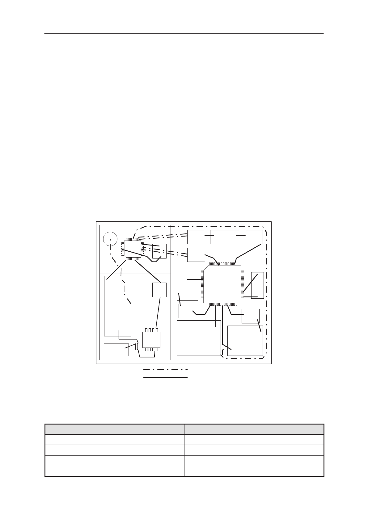
The RF in the RAE–2 GSM is based on the architecture used in DCT 3.
The RAE–2 RF Engine (figure below) is a single side design, on the
A–side, with all components located under the PDA unit. Shielding com-
prises three shielding cans with removable lids. The maximum building
height for the RF Engine is 2 mm.
BS8_RF
ANT
CRFU
DUPLEX
Detect
RF Characteristics
SAW
SAW
PA
RX
TX
Match Match
116MHz
232MHz
VCO
Loop
Filter
13MHz
VCTCXO
71MHz
SAW
SUMMA
stripline
ustripline
13MHz
CER
Loop
Filter
UHF
VCO
Table 1. Main RF characteristics
Item Values
Receive frequency range 935 ... 960 MHz
Transmit frequency range 890 ... 915 MHz
Duplex spacing 45 MHz
Channel spacing 200 kHz
Original 02/99
Page 3 – 5
Page 6
RAE–2
PAMS
BS8_RF
Table 1. Main RF characteristics (continued)
Number of RF channels 124
Power class 4
Number of power levels 15
Technical Documentation
ValuesItem
Note 1 : Standard of primary GSM 900 Band, P – GSM
890 – 915 MHz : Mobile transmit, Downlink
935 – 960 MHz : Mobile receive, Uplink
Transmitter Characteristics
Item Values
Type Upconversion, nonlinear, FDMA/TDMA
Intermediate frequency ( phase modulated ) 116 MHz
LO frequency range 1006 ... 1031 MHz
Output power 2 W peak ( 33 dBm )
Power control range min. 5 ... 33 dBm
Maximum phase error ( RMS/peak ) max 5 deg./20 deg. peak
Output power
Parameter Min. Typ. Max. Unit / Notes
Max. output power 33.0 dBm
Max. output power tolerance
(power level 5)
Output power tolerance /
power levels 6...15
Output power tolerance /
power levels 16...19
Output power control step
size
0.5 2.0 3.5 dB
Note 1 : Output power refers to the measure of power when averaged over the useful part of the burst. Power levels are measured at the antenna connector.
+/– 2.0
+/– 2.5
+/– 3.0
+/– 4.0
+/– 5.0
+/– 6.0
dB, normal cond.
dB, extreme cond.
dB, normal cond.
dB, extreme cond.
dB, normal cond.
dB, extreme cond.
Note 2 : Interval between power steps shall be 2 +/–1.5 dB
Page 3 – 6
Original 02/99
Page 7

PAMS
RAE–2
Technical Documentation
Receiver characteristics
Item Values
Type Linear, FDMA/TDMA
IF frequencies 1st 71 MHz, 2nd 13 MHz
LO frequencies 1st LO 1006 ... 1031 MHz, 2nd LO 58 MHz
Typical 1 dB bandwidth +/– 90 kHz
Sensitivity min. – 102 dBm , S/N >8 dB
Total typical receiver voltage gain ( from anten-
na to RX ADC )
Receiver output level ( RF level –95 dBm ) 50 mVpp ( typical balanced signal level of 13
Typical AGC range (dynamic range –93dB) –17 ... +40 dB
73 dB
MHz
IF in RF BB interface = input level to RX ADCs )
BS8_RF
Accurate AGC control range 57 dB
Typical AGC step in LNA –15 dB
Usable input dynamic range –102 ... –10 dBm
RSSI dynamic range –110 ... –48 dBm
AGC relative accuracy on channel ( accurate
range )
Compensated gain variation in receiving band +/– 1.0 dB
+/– 0.8 dB
Original 02/99
Page 3 – 7
Page 8

RAE–2
PAMS
BS8_RF
DC characteristics
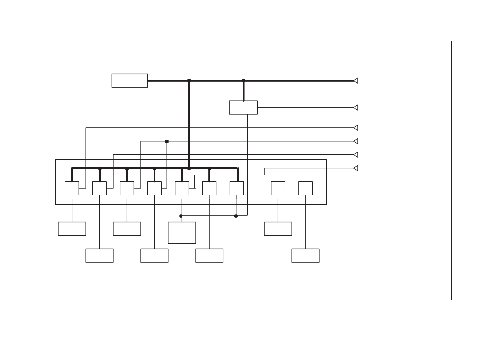
Regulators
Transceiver has got a multi function power management IC, which con-
tains among other functions, also 7 pcs of 2.8 V regulators. All regulators
can be controlled individually with 2.8 V logic directly or through control
register. In GSM direct controls are used to get fast switching, because
regulators are used to enable RF–functions.
Use of the regulators can be seen in the power distribution diagram.
CCONT also provides 1.5 V reference voltage for SUMMA and CRFU1a
( and for DACs and ADCs in COBBA too ).
All control signals are coming from MAD and they are 2.8 V logic signals..
Technical Documentation
Page 3 – 8
Original 02/99
Page 9
Original 02/99
3.6 V
Power distribution diagram
PAMS
Technical Documentation
Page 3 – 9
C–CONT
VR
1
2.3 mA
VCTCXO
BUFFER
VXO
VR
2
51 mA
CRFU,
SUMMA
VRX
BATTERY
VR
3
18 mA
PLLs
VSYN_2
VR
4
19.5 mA
VCOs
BUFFERS
VSYN_1
VR
5
84 mA
CRFU,
SUMMA
VTX
VR
6
COBBA
ANAL.
1.6 A
PA
VR
7
VREF V5V
0.1 mA
SUMMA
CRFU
VREF_1
VREF_2
1 mA
CHARGE
PUMPs
VCP
VBATT
TXP
VXOENA
SYNPWR
RXPWR
TXPWR
BS8_RF
RAE–2
Page 10

RAE–2
PAMS
BS8_RF
Functional descriptions
RF block diagram
The RF block comprises a conventional dual conversion receiver and the
transmitter features an up–conversion mixer for the final TX–frequency.
The architecture contains three ICs. Most of the functions are horizontally
and vertically integrated. UHF functions except power amplifier and VCO
are integrated into CRFU_1a, which is a BiCMOS–circuit suitable for
LNA– and mixer–function. Most of the functions are in SUMMA, which
also is a BiCMOS–circuit. SUMMA is a IF–circuit including IQ–modulator
and PLLs for VHF– and UHF–synthesizers.
Power amplifier is also an ASIC, it is a so called MMIC ( monolithic mi-
crowave integrated circuit ). It has got three amplifier stages including in-
put and interstage matchings. Output matching network is external. Also
TX gain control is integrated into this chip.
Technical Documentation
See block diagram next page
Page 3 – 10
Original 02/99
Page 11
PAMS
RAE–2
Technical Documentation
SUMMA
TQFP–48
BS8_RF
Original 02/99
antenna
Figure 1.
ext.ant.conn.
Power amplifier
two way switch
Page 3 – 11
Page 12

RAE–2
PAMS
BS8_RF
Frequency synthesizers
Both VCOs are locked with PLLs into stable frequency source, which is a
VCTCXO–module ( voltage controlled temperature compensated crystal
oscillator ). The VCTCXO is running at 13 MHz. Temperature effect is
controlled with AFC ( automatic frequency control ) voltage, the VCTCXO
is locked into the frequency of the base station. AFC is generated by
baseband with a 11 bit conventional DAC in COBBA.
The UHF PLL is located in the SUMMA. There is 64/65 (P/P+1) prescal-
er, N– and A–divider, reference divider, phase detector and charge pump
for the external loop filter.
The UHF local signal is generated by a VCO–module ( VCO = voltage
controlled oscillator ) and sample of frequency of VCO is fed to prescaler.
The prescaler is a dual modulus divider. The output of the prescaler is
fed to the N– and A–dividers, which produce the input to phase detector.
The phase detector compares this signal to reference signal, which is di-
vided with reference divider from VCTCXO output. Output of the phase
detector is connected into charge pump, which charges or discharges in-
tegrator capacitor in the loop filter depending on the phase of the mea-
sured frequency compared to reference frequency.
Technical Documentation
The loop filter filters out the pulses and generates the DC to control the
frequency of UHF–VCO. The loop filter defines step response of the PLL
( settling time ) and effects to stability of the loop, that’s why integrator ca-
pacitor has got a resistor for phase compensation.
The other filter components are for sideband rejection. Dividers are con-
trolled via serial bus. SDATA is for data, SCLK is serial clock for the bus
and SENA1 is a latch enable, which stores new data into dividers. The
UHF–synthesizer is the channel synthesizer, so the channel spacing is
200 kHz. 200 kHz is the reference frequency for the phase detector.
Page 3 – 12
Original 02/99
Page 13

PAMS
RAE–2
Technical Documentation
R
f
ref
f_out /
VHF PLL is also located into SUMMA. It comprises a 16/17 ( P/P+1 )
dual modulus prescaler, N– and A–dividers, reference divider, phase de-
tector and charge pump for the loop filter. The VHF local signal is gener-
ated with a discrete VCO–circuit. The VHF PLL works in the same way
as UHF–PLL. The VHF–PLL is locked on fixed frequency, so higher ref-
erence frequency is used to decrease phase noise.
M
PHASE
DET.
CHG.
PUMP
Kd
freq.
reference
AFC–controlled VCTCXO
LP Kvco
VCO
M = A(P+1) + (N–A)P=
M
BS8_RF
f_out
NP+A
Receiver
Receiver is a dual conversion linear receiver.
The received RF–signal from the antenna is fed via the duplex filter to
LNA ( low noise amplifier ) in CRFU_1a. Active parts (RF–transistor and
biasing and AGC–step circuitry) are integrated into this chip. Input and
output matching networks are external.
Gain selection is carried out with PDATA0 control. Gain step in LNA is
activated when the RF–level in the antenna is about –45 dBm.
After the LNA amplified signal ( with low noise level ) is fed to bandpass
filter, which is a SAW–filter ( SAW, surface acoustic wave ).
This bandpass filtered signal is then mixed down to 71 MHz, which is the
first intermediate frequency. The 1st mixer is located into CRFU_1a
ASIC. This integrated mixer is a double balanced Gilbert cell. All active
parts and biasing are integrated and matching components are external.
Because this is an axtive mixer it also amplifies IF–frequency. Also local
signal buffering is integrated and upper side injection is used. First local
signal is generated by the UHF–synthesizer.
The first IF–signal is then bandpass filtered with a selective SAW–filter.
From the mixer output to the IF–circuit input the signal path is balanced.
The IF–filter provides selectivity for channels greater than +/–200 kHz.
Also it attenuates image frequency of the second mixer and intermodulat-
Original 02/99
Page 3 – 13
Page 14

RAE–2
PAMS
BS8_RF
Technical Documentation
ing signals. Selectivity is required in this place, because of needed lineari-
ty and adjacent channel interferers will be on too high signal level for the
stages following.
The next stage in the receiver chain is AGC–amplifier. It is integrated into
SUMMA–ASIC. The AGC has got analog gain control. The control volt-
age for the AGC is generated with DA–converter in COBBA in baseband.
AGC–stage provides accurate gain control range ( min. 57 dB ) for the
receiver.
After the AGC there is the second mixer, which generates the second in-
termediate frequency, 13 MHz. The local signal is generated in SUMMA
by dividing VHF–synthesizer output ( 232 MHz ) by four, so the 2nd LO–
frequency is 58 MHz.
The 2nd IF–filter is a ceramic bandpass filter at 13 MHz. It attenuates ad-
jacent channels, except for +/– 200 kHz there is not much attenuation.
Those +/– 200 kHz interferers are filtered digitally by the baseband. So
the RX DACs are so good, that there is enough dynamic range for the
faded 200 kHz interferer. Also the whole RX has to be able to handle sig-
nal levels in a linear way
After the 13 MHz filter there is a buffer for the IF–signal, which also con-
verts and amplifies single ended signal from filter to balanced signal for
the buffer and AD–converters in COBBA. Buffer in SUMMA has got volt-
age gain of 36dB and buffer gain setting in COBBA is 0 dB. It is possible
to set gainstep ( 9.5 dB ) into COBBA via control bus, if needed..
Transmitter
The transmitter chain consists of IQ–modulator, upconversion mixer, pow-
er amplifier and there is a power control loop.
I– and Q–signals are generated by baseband in COBBA–ASIC. After
post filtering ( RC–network ) they are fed into IQ–modulator in SUMMA. It
generates modulated TX IF–frequency, which is VHF–synthesizer output
divided by two, that is 116 MHz. The TX–amplifier in SUMMA has two se-
lectable gain levels. Output is set to maximum via control register of
SUMMA. After SUMMA there is a bandpass LC–filter for noise and har-
monic filtering before the signal is fed for upconversion into final TX–fre-
quency in CRFU_1a.
Upconversion mixer in CRFU_1a is a so called image reject mixer. It at-
tenuates the unwanted sideband in the upconverter output. The mixer
itself is a double balanced Gilbert cell. The phase shifters required for
image rejection are also integrated. The local signal needed in upconver-
sion is generated by the UHF–synthesizer, but buffers for the mixer are
integrated into CRFU_1a.
The output of the upconverter is buffered and matching network makes a
single ended 50 ohm impedance.
The next stage is a TX interstage filter, which attenuates the unwanted
signals from the upconverter, mainly LO–leakage and image frequency
Page 3 – 14
Original 02/99
Page 15

PAMS
RAE–2
Technical Documentation
from the upconverter. Also it attenuates the wideband noise. This band-
pass filter is a SAW–filter.
The final amplification is carried out by the third IC, the power amplifier
which is a MMIC. It features a 50 ohm input, output requires an external
matching network. The MMIC comprises three amplifier stages and inter-
stage matchings. Also included is a gain control, which is controlled with a
power control loop. The PA features over 35 dB power gain and it is able
to produce 2.5 W into output with 0 dBm input level. The gain control
range is over 35 dB to get desired power levels and power ramping up
and down.
The harmonics generated by the nonlinear PA ( class AB ) are filtered out
with the matching network and lowpass/bandstop filtering in the duplexer.
Bandstop is required because of wideband noise located on RX–band.
Power control circuitry consists of a power detector in the PA output and
an error amplifier in SUMMA. There is a directional coupler connected
between the PA–output and the duplex filter. It takes a sample from the
forward going power with certain ratio. This signal is rectified in a schott-
ky–diode and it produces a DC–signal signal after filtering. This peak–de-
tector is linear on absolute scale, except it saturates on very low and high
power levels – it produces a S–shape curve.
BS8_RF
This detected voltage is compared in the error–amplifier in SUMMA to
TXC–voltage, which is generated by DA–converter in COBBA. Because
also gain control characteristics in PA are linear in absolute scale, control
loop defines a voltage loop, when closed. The closed loop tracks the
TXC–voltage quite linearly.
4
– function ), which reduces
The TXC has got a raised cosine form ( cos
switching transients, when pulsing power up and down. Because dynam-
ic range of the detector is not wide enough to control the power ( actually
RF output voltage ) over the whole range, there is a control named TXP
to work under detected levels. Burst is enabled and set to rise with the
TXP until the output level is high enough, that feedback loop works. The
loop controls the output via the control pin in the PA MMIC to the desired
output level and burst has got the waveform of TXC–ramps. Because
feedback loops could be unstable, this loop is compensated with a domi-
nating pole. This pole decreases gain on higher frequencies to get phase
margins high enough.
Original 02/99
Page 3 – 15
Page 16

RAE–2
PAMS
BS8_RF
RF_OUT
DETECTOR
Technical Documentation
PADIR.COUPLER
RF_IN
K
cp
R1
K
K
det
R2
= –R1/R2
ERROR
AMPLIFIER
R
K
PA
C
DOMINATING
POLE
AGC strategy
The AGC–amplifier is used to maintain output level of the receiver almost
constant.
AGC has to be set before each received burst, this is called pre–monitor-
ing. The receiver is switched on before the burst begins, the DSP mea-
sures received signal level and adjusts RXC, which controls RX AGC–
amplifier or it switches off the LNA with PDATA0 control line. This pre–
monitoring is done in three phases and this sets the settling times for RX
AGC. Pre–monitoring is required because of linear receiver, received sig-
nal must be in full swing, no clipping is allowed and because DSP doesn’t
know, what is the level going to be in next burst.
There is at least 60 dB accurate gain control ( continuous, analog ) and
one digital step in LNA. It is typically about 30...35 dB.
RSSI must be measured on range –48...–110 dBm. After –48 dBm level
MS reports to base station the same reading.
Because of RSSI–requirements, gain step in LNA is used roughly on –45
dBm RF–level and up to –10 dBm input RF–level accurate AGC is used
to set RX output level. LNA is ON ( PDATA0 = ”0” ) below –47 dBm. from
–47 dBm down to –95 dBm
Figure 2. Power control feedback loop
TXC
This accurate AGC in SUMMA is used to adjust the gain to desired value.
RSSI–function is in DSP, but it works out received signal level by measur-
ing RX IQ–level after all selectivity filtering ( meaning IF–filters, Σ∆±con-
verter and FIR–filter in DSP). So 50 dB accurate AGC dynamic range is
Page 3 – 16
Original 02/99
Page 17

PAMS
RAE–2
Technical Documentation
required. Remaining 10 dB is for gain variations in RX–chain ( for calibra-
tion )
Below –95 dBm RF–levels, output level of the receiver drops dB by dB.
At –95 dBm level output of the receiver gives 50 mVpp. This is the target
value for DSP. Below this it drops down to ca. 9 mVpp @ –110 dBm RF–
level.
This strategy is chosen because we have to roll off the AGC in PLUSSA
early enough, that it won’t saturate in selectivity tests. Also we can’t start
too early, then we will sacrifice the signal to noise ratio and it would re-
quire more accurate AGC dynamic range. 50 mVpp target level is set,
because RX–DAC will saturate at 1.4 Vpp. This over 28 dB headroom is
required to have margin for +/– 200 kHz faded adjacent channel ( ca. 19
dB ) and extra 9 dB for pre–monitoring.
Production calibration is done with two RF–levels, LNA gain step is not
calibrated. The gain changes in the receiver are taken off from the dy-
namic range of accurate AGC. Variable gain stage in SUMMA is designed
in a way, that it is capable of compensating itself, there is good enough
margin in AGC.
BS8_RF
AFC function
AFC is used to lock the transceivers clock to the frequency of the base
station.
AFC–voltage is generated in the COBBA with a 11 bit AD–converter.
There is a RC–filter in AFC control line to reduce the noise from the con-
verter. Settling time requirement for the RC–network comes from signal-
ling, how often PSW ( pure sine wave ) slots occur. They are repeated af-
ter 10 frames , meaning that there is PSW in every 46 ms.
AFC tracks the base station frequency continuously, so the transceiver
has got a stable frequency, because changes in the VCTCXO–output
don’t occur so fast ( temperature ).
Settling time requirement comes also from the start up–time allowed.
When transceiver is in sleep mode and ”wakes” up to receive mode ,
there is only about 5 ms for the AFC–voltage to settle. When the first
burst comes in system clock has to be settled into +/– 0.1 ppm frequency
accuracy. Settling time requirement comes also from the start up–time al-
lowed. When transceiver is in sleep mode and ”wakes” up to receive
mode , there is only about 5 ms for the AFC–voltage to settle. When the
first burst comes in system clock has to be settled into +/– 0.1 ppm fre-
quency accuracy.
The VCTCXO–module requires also 5 ms to settle into final frequency.
Amplitude rises into full swing in 1 ... 3 ms, but frequency settling time is
longer so this oscillator must be powered up early enough.
Original 02/99
Page 3 – 17
Page 18

RAE–2
PAMS
BS8_RF
RF block requirements
Duplex filter
Parameter Transmit section Receive section unit
Center frequency,
ftx,frx
BW ( bandwidth ) at
passband
Maximum insertion
loss at BW
Ripple at BW, peak to
peak
Terminating impedance
Maximum VSWR 2.2 1.8
ftx : 902.5 frx : 947.5 MHz
+/– 12.5 +/– 12.5 MHz
1.6 ( at +25 deg. C )
1.9 ( at –20...+85 deg. C )
1.1 1.5 dB
50 50 ohms
Technical Documentation
3.2 ( at +25 deg. C )
3.7 ( at –20...+85deg. C )
dB
Minimum attenuations
Permissible input pow-er4.0 AVG (12.5% duty cyclr) W
Freq.range Att. Freq.range Att.
925...935 3 3...200 30 MHz/dB
935...960 15 200...500 16 MHz/dB
1780...1830 28 500...890 25 MHz/dB
2670...2745 35 890...915 26 MHz/dB
980...1000 21 MHz/dB
1000...1050 23 MHz/dB
1400...1500 35 MHz/dB
Part no: NMP code 4512075
Receiver blocks
LNA in CRFU_1a
Parameter Min. Typ. Max. Unit/Notes
Frequency band 935 – 960 MHz
Supply voltage 2.7 2.8 2.855 V
Current consumption 8 mA
Insertion gain 17.5 18.5 19.5 dB
Noise figure 1.7 2.2 dB,PDATA0=H
Input 1 dB compression point –19 dBm, PDATA0=H
Reverse isolation 15 dB
Input VSWR 2
Page 3 – 18
Original 02/99
Page 19

PAMS
RAE–2
Technical Documentation
Unit/NotesMax.Typ.Min.Parameter
Output VSWR 2
Gain reduction 30 35 dB,room temp.
Step accuracy –2 +2 dB,over temp.range
Noise figure, when PDATA=0 20 dB
BS8_RF
RX interstage filter
Parameter Min. Typ. Max. Unit
Passband 935 – 960 MHz
Insertion loss 3.3 dB
Ripple in passband 1.3 dB
Attenuation DC...890 MHz 45 dB
Attenuation 890...915 MHz 25 dB
Attenuation 980...1030 MHz 25 dB
Attenuation 1025...3000 MHz 35 dB
Terminating impedance UNBALANCED–BALANCED
50/50
VSWR 2.0
Maximum drive level +15 dBm
Part no: NMP code 4511049
1st mixer in CRFU_1a
Parameter Min. Typ./
Nom.
Supply voltage 2.7 2.8 2.85 V
Current consumption 9 mA
RX frequency range 935 960 MHz
LO frequency range 1006 1031 MHz
IF frequency 71 MHz
Insertion gain 9 12 dB
NF, SSB 1 1.5 dB
IIP3 0 dBm
Max. Unit/Notes
ohm
1 dB input compression point –10 dBm
IF/2 spurious level –30 dBm, *
LO power level in RF–port –25 dBm
Input VSWR 2
Output resistance (balanced) 10 k ohm
Output capacitance (bal-
anced)
1.2 pF
Original 02/99
Page 3 – 19
Page 20

RAE–2
PAMS
BS8_RF
Technical Documentation
1st IF–filter
Parameter min. typ. max. unit
Operating temperature range –20 +75 deg.C
Center frequency , fo 71 MHz
Maximum ins. loss at 1dBBW 11 dB
Group delay ripple at +/–90 kHz BW 1.3 us pp
Bandwidths relative to 71 MHz
1 dB bandwidth
3 dB bandwidth
5 dB bandwidth
22 dB bandwidth
30 dB bandwidth
40 dB bandwidth
Spurious rejection, fo +/– 26 MHz 65 dB, *
Terminating impedance ( balanced )
resistance input
resistance output
capacitance ( parallel ) input
capacitance ( parallel) output
+/– 70
+/–120
+/– 230
+/– 350
+/– 550
+/– 700
1.1
1.2
15.6
10.6
kHz
kohm
kohm
pF
pF
* Matching network included. NMP part no. 4510137
AGC–stage and 2nd mixer in SUMMA
Parameter Min. Typ. Max. Unit/Notes
Supply voltage 2.7 2.8 2.85 V
Current consumption 27 32 mA
Input frequency range 45 120 MHz
2nd IF frequency range 0.4 17 MHz
Total noise figure, SSB,
max. gain
Total noise figure, SSB,
min. gain
Max. voltage gain 40 dB
Min. voltage gain –20 dB
Control voltage for min. gain 0.5 V
Control voltage for max. gain 1.4 V
Output 1 dB compression
point @ max. gain
Input 1 dB compresion point
@ min. gain
IF input impedance (bal-
anced)
2nd mixer output impedance
( single output )
800 mVpp
80 mVpp
2.4/tbd 3.8/2 5.6/tbd kohm/pF
15 dB,
65 dB,
100 ohm
Page 3 – 20
Original 02/99
Page 21

PAMS
RAE–2
Technical Documentation
2nd IF Filter
Parameter min. typ. max. unit
Center frequency, fo 13 MHz
1 dB bandwidth, 1dBBW
( relative to 13 MHz )
Insertion loss 6.0 dB
Amplitude ripple at 1dBBW 1.0 dB
Group delay ripple at 1 dB
BW, peak to peak
Attenuations, relative to
13 MHz
fo +/– 400 kHz
fo +/– 600 kHz
fo +/– 800 kHz
Terminating impedance 313 330 347 ohm
+/– 90 kHz
1.5 us
dB
25
35
45
BS8_RF
NMP part no. 4510009
Buffer in SUMMA for 2nd IF
Parameter Min. Typ. Max. Unit
Input frequency range 0.4 17 MHz
Voltage gain ( single ended
input and balanced output )
1 dB output compression
point ( Rload=10 kohm balanced )
Input impedance 3.3/4 kohm/pF
Output impedance, balanced 600 ohm
34 36 38 dB
1.4 Vpp
Original 02/99
Page 3 – 21
Page 22

RAE–2
PAMS
BS8_RF
Technical Documentation
Transmitter blocks
IQ–modulator and TX–AGC in SUMMA
Parameter Min. Typ. Max. Unit
Supply voltage 2.7 2.8 2.85 V
Current consumption 28 tbd. mA
Modulator Inputs (I/Q) Minimum Typical /
Nominal
Input bias current (balanced) 100 nA
Maximum Unit / Notes
Input common mode voltage 0.8 V
Input level (balanced) 1.2 Vpp
Input frequency range 0 300 kHz
Input resistance (balanced) tbd kohms
Input capacitance (balanced) 2 pF
IQ–input phase balance
total, temperature included
IQ–input phase balance
temperature effect
IQ–input amplitude balance
total, temperature included
IQ–input amplitude balance
temperature effect
Modulator Output Minimum Typical /
Output frequency 85 400 MHz
Output power, high (bal-
anced, into 100 ohm)
NOTE: Requires input level of
1.1 Vpp (difrential)
–4 4 deg.
–2 2 deg.
–0.5 0.5 dB
–0.2 0.2 dB
Maximum Unit / Notes
Nominal
–5 –3 dBm
Output power, low (balanced,
into 100 ohm )
NOTE: Requires input level of
1.1 Vpp (diff.)
Noise level in output –145 dBm/Hz avg.
Total gain control range 35 dB
Gain step 5 dB
–10 –8 dBm
Page 3 – 22
Original 02/99
Page 23

PAMS
RAE–2
Technical Documentation
MinimumModulator Output
Nominal
Absolute gain accuracy –2 +2 dB
Any gain step up/down set-
tling time
Output 3rd Order Intermo-
dulation products, when both
wanted signals are at the level of –12 dBm at the output
10 usec
–35 dB
Unit / NotesMaximumTypical /
116 MHz LC TX IF–filter
Parameter Min. Typ. Max. Unit
Center frequency 116 MHz
Insertion loss @ 116 MHz 3.7 dB
Relative attenuation @ +/– 10
MHz offset
Relative attenuation @ +/– 20
MHz offset
Relative attenuation @ 232
MHz
Relative attenuation @ 348
MHz
Relative attenuation @
464–1000 MHz
Input impedance, balanced 100 ohm
5 dB
8 dB
15 dB
20 dB
25 dB
BS8_RF
Output impedance, balanced 200 ohm
Upconversion mixer and in CRFU_1a
Parameter Min. Typ. Max. Unit
Supply voltage 2.7 2.8 2.85 V
Supply current 50 mA
Input frequency 116 MHz
Input level –5 –8 dBm
Output frequency range 890 915 MHz
Output level +3 +5 dBm
NF,SSB 20 dB
LO–signal level in output –29 dBc
Unwanted sideband level –15 dBc
fLO+/–2xIF spurious level –40 dBc
7x116 MHz spurious level –40 dBc
Original 02/99
Page 3 – 23
Page 24

RAE–2
PAMS
BS8_RF
8x116 MHz spurious level –55 dBc
Input impedance (balanced) 600//2 ohm//pF
Output VSWR, ( with match-
ing network and output balun)
2
Technical Documentation
UnitMax.Typ.Min.Parameter
TX interstage filter
Parameter Min. Typ. Max. Unit
Passband 890 – 915 MHz
Insertion loss 3.8 dB
Ripple in passband 1.5 dB
Attenuation DC...813 MHz 35 dB
Attenuation 925...935 MHz 7 dB
Attenuation 935...960 MHz 15 dB
Attenuation 1006...1031 MHz 40 dB
Attenuation 1122...1147 MHz 45 dB
Attenuation 1780...1830 MHz 10 dB
Attenuation 2670...2745 MHz 10 dB
Terminating impedance 50 ohm
VSWR 2.5
Maximum drive level +15 dBm
NMP part no. 4511015
Power amplifier MMIC
Parameter Symbol Test condition Min Typ Max Unit
Operating freq. range 880 915 MHz
Supply voltage Vcc 3.0 3.5 5.0 V
Auxiliary supply voltage Vreg 2.7 2.8 2.9 V
Auxiliary supply current Ireg tdb. mA
Input power Pin Pout=35.0 dBm, Vcc=3.5 V,
Vpc=2.2 V,
Output power Pout Pin= 0 dBm, Vcc=3.0 V,
Vpc=2.2 V, Tamb=+85 deg.C
Gain control range
( overall dynamic
range)
Gain control slope
( sensitivity at the linear
range )
S Vpc1 @10 Vpeak output volt.
Vpc= 0.5 ... 2.2 V 45 dB
Vpc2 @0.5 Vpeak output volt.
S=((10–0.5)/(Vpc1–Vpc2))
V/V, Pin = 0...+5dBm
0 2 5 dBm
34.2 dBm
20 tbd. 40 V/V
Page 3 – 24
Original 02/99
Page 25

PAMS
RAE–2
Technical Documentation
Isolation Vcc=3.5 V, Vpc=0.2 V, Pin=0
dBm
Carrier switching time tr, tf Vcc=3.5 V, Pin=0 dBm
Vpc is a pulse from 0.2 to 2.2
V. Rise time up to –0.5 dB
from the final power. Fall time
vice versa.
Total efficiency η Pin= 0 dBm , Pout= +34.3
dBm, Vcc=3.5 V,
Tamb = + 25 deg. C
Control current Ipc
Harmonics –35 dBc
Input VSWR
VSWRi1 Pin= 0...+5 dBm , Pout=
VSWRi2 Pin= 0...+5 dBm , Pout= +6.0
Pin= 0...+5 dBm , Pout=
+34.8 dBm, Vcc=3.5 V
+34.0 dBm, Vcc=3.5 V
... +32.0 dBm, Vcc=3.5 V
Vpc adjusted for desired
power levels
50 %
BS8_RF
–40 dB
1 us
+/– 3 mA
peak
2:1
4:1
UnitMaxTypMinTest conditionSymbolParameter
Leakage current Ileak Vcc=3.5 V, Vpc=0 V,
Vreg=0 V, no RF–drive
Intermodulation distorsion
AM–PM conversion Kp Pin= –2.0 ... +5.0 dBm,
Receive band noise
power
Stability Pin= 0 dBm+/–3dBm,
Load mismatch stress Pin= 0 dBm, Vcc=5.0 V,
IMD Pinwant= 0 dBm @ 915 MHz
Pinint = –50 dBm @ 905 MHz
Poutwant= +34.8 dBm
Vcc=3.5 V,
Poutint @905 MHz
Poutimd @925 MHz
IMD=Poutint – Poutimd,
Tamb = + 25 deg. C
Pout= +6.0 ... +34.0 dBm
Vpc adjusted for desired out-
put power levels
Vcc=3.0 V
Pn Vcc=3.5 V , RBW=30kHz
Pout = +34.8 dBm, Freq.
band: 925...960 MHz
Vcc=3.0...5.0 V,
Vpc=0 ... 2.2 V
Load VSWR 12:1, all phases
Pout=Pmax
Load VSWR 20:1, all phases
10 uA
5 dB
3 deg/dB
–80 dBm
All spurious outputs more than 65
dB below desired signal
No module damage
Original 02/99
Page 3 – 25
Page 26

RAE–2
PAMS
BS8_RF
Technical Documentation
Directional coupler
Parameter Min. Typ. Max. Unit/Notes
Frequency range 890 915 MHz
Insertion loss 0.5 dB
Coupling factor 15 dB
Directivity 13 14 dB
Impedance level of the
main line
VSWR on main line 1.6
Impedance level of the
coupled line
50 ohm
50 ohm
NMP part no. 4551001
Power detector
Parameter Min. Typ. Max. Unit/Notes
Supply voltage 2.7 2.8 2.85 V
Supply current 2.0 mA
Frequency range 890 915 MHz
Dynamic range 45 dB
Linear range, * 35 dB
Bias current for detector
diode
Input power range, ** –8 20 dBm
Output voltage 0.1 2.2 V
Variation of the detected volt-
age over temperature range
Load resistance 10 kohm
40 uA
0.7 mV/_C
* RF input voltage versus detected output voltage
* * Directional coupler coupling factor 14 dB
Power control section in SUMMA, closed loop characteristics
Parameter Min. Typ. Max. Unit/Notes
Supply voltage 2.7 2.8 2.85 V
Supply current tbd. mA
TXP input voltage, LOW 0.5 V
TXP input voltage, HIGH 2.4 V
Detector input voltage 0.1 2.2 V
TXC input voltage 0.1 2.2 V
Page 3 – 26
Original 02/99
Page 27

PAMS
RAE–2
Technical Documentation
TXC and TXP input resistance
TXC and TXP input capacitance
Output voltage (POP & POG) 0.5 2.2 V
POP– and POG–output im-
pedance
POP and POG –output cur-
rent driving capability
Switch on resistance (bet–
ween INL& POP or POG)
Voltage of POP/POG when
inactive (max. 3.5mA sink)
Offset of OP1 and OP2
op.amp.
Temperature coefficient of the
offset voltage
Bandwidth ( OP1 & OP2 ),
unity gain
Open loop gain 20 dB
50 kohm
4 pF
50 ohm
+/– 4 mA
tbd. ohm
0.1 V
–40 40 mV
30 uV/deg.C
6 MHz
BS8_RF
Unit/NotesMax.Typ.Min.Parameter
Closed loop gain 15 dB
Closed loop –3 dB bandwidth 70 kHz
Phase margin 45 60 degrees
Gain margin 30 dB
Synthesizers blocks
VCTCXO, reference oscillator
Parameter Min. Typ. Max Unit/.Notes
Supply voltage, Vcc 2.70 2.80 2.85 V
Current consumption, Icc 1.5 mA
Operating temperature range –20 +75 deg. C
Nominal frequency 13 MHz
Output voltage swing
( swing of 13 MHz component, selective measurement from the spectrum )
800 mVpp
Load, resistance
capacitance
Frequency tolerance @+25 deg. C – 1.0 + 1.0 ppm
Frequency tolerance after reflow
( @ +25 deg. C )
– 2.0 + 2.0 ppm
Original 02/99
2
10
kohm
pF
Page 3 – 27
Page 28
RAE–2
PAMS
BS8_RF
Frequency stability vs. temperature
( ref. @+25 , –20....+75 deg. C )
Frequency stablity vs. supply voltage ( 2.8 V +/– 100 mV )
Frequency stability vs. load change
( 2 kohm//10 pF +/– 10 % )
Aging – 1.0 + 1.0 ppm/year
Nominal control voltage, Vc 1.15 V
Voltage control range 0.0 2.3 V
Voltage control characteristics
( see note 1. )
Vc input resistance 1 Mohm
Frequency adjustment +/–
Harmonics ( with 2 kohm//10 pF ) – 5 dBc
– 5.0 + 5.0 ppm
– 0.1 + 0.1 ppm
– 0.3 + 0.3 ppm
+/– 12 +/– 24 ppm/V when
3.0
Technical Documentation
Unit/.NotesMaxTyp.Min.Parameter
0.3 V<Vc<2.3 V
ppm with inter–
nal trimmer
Start up time
output level within 90%
output frequency limits +/–0.05ppm
from the final value
Phase noise @ 1 kHz offset –130 dBc/Hz
5
5
ms
VHF PLL in SUMMA
The same VHF VCO and also the same frequency is used so the VHF
PLL is common.
Table 2. VHF–synthesizer, specification
Parameter Min. Typ. Max. Unit/Notes
Start up settling time 3.0 ms
Phase error 1 deg./rms
Sidebands
+/– 1 MHz
+/– 2 MHz
+/– 3 MHz
> +/– 3.0 MHz
Table 3. VHF PLL block in SUMMA, specification
–70
–80
–80
–90
dBc
Parameter Min. Typ. Max. Unit/notes
Input frequency range 150 500 MHz
Input signal level 80 800 mVpp
Input resistance tbd. kohm
Input capacitance tbd. pF
Supply current 3.5 mA
Reference input frequency 30 MHz
Page 3 – 28
Original 02/99
Page 29

PAMS
RAE–2
Technical Documentation
Table 3. VHF PLL block in SUMMA, specification (continued)
Unit/notesMax.Typ.Min.Parameter
Phase comparison frequency 1 MHz
Charge pump output
current 1
current 2
Sink to source current matching error of the charge pump
Charge pump current error +/– 10 %
Charge pump min. output
voltage
Charge pump max. output
voltage
Charge pump leakage current 5 nA
Phase detector phase noise
level
0.5
2.0
+/– 5 %
0.5 V
*
Vcp–0.5
–163 dBc/Hz
mA
V
BS8_RF
*Vcp = 5V
VHF VCO and low pass filter
Parameter Min. Typ. Max. Unit/Notes
Supply voltage range 2.7 2.8 2.85 V
Current consumption 4 7 mA
Control voltage 0.5 4.0 V
Operation frequency 232 MHz
Output level –13 –10 dBm ( output after
the lowpass filter )
Harmonics –30 dBc, ( filtered )
Phase noise,
fo +/– 600 kHz
fo +/– 1600 kHz
fo +/– 3000 kHz
Control voltage sensitivity 8.0 14.0 MHz/V
Pushing figure +/– 2 MHz/V
Frequency stability +/– 3 MHz ( over temper-
Spurious content –70 dBc
–120
–130
–140
dBc
ature range –10...+75 C deg.)
Original 02/99
Page 3 – 29
Page 30

RAE–2
PAMS
BS8_RF
Technical Documentation
UHF PLL
Table 4. UHF–synthesizer,
Parameter Min. Typ. Max. Unit/Notes
Start up settling time 3.0 ms
Settling time +/– 25 MHz 500 800 us, ( into +/– 20 Hz
from final frequency )
Phase error 3.7 deg./rms
Sidebands
+/– 200 kHz
+/– 400 kHz
+/– 600...+/–1400 kHz
+/–1.4... +/– 3.0 MHz
> +/– 3.0 MHz
Table 5. UHF PLL block in SUMMA
Parameter Min. Typ. Max. Unit/notes
Input frequency range 650 1700 MHz
–40
–60
–66
–76
–86
dBc
Input signal level (f<1.5 GHz) 200 mVpp
Input resistance tbd. kohm
Input capacitance tbd. pF
Supply current 8 mA
Reference input frequency 30 MHz
Reference input level 100 mVpp
Reference input impedance tbd.
Phase comparison frequency 1 MHz
Charge pump output
current 1
current 2
Sink to source current matching error of the charge pump
Charge pump current error +/– 10 %
Charge pump current temper-
ature variation
Charge pump leakage current 5 nA
Phase detector phase noise
level
0.5
2.0
+/– 5 %
tbd. %
–163 dBc/Hz
mA
UHF VCO module
Parameter Conditions Rating Unit/
Supply voltage, Vcc 2.8 +/– 0.1 V
Supply current, Icc Vcc = 2.8 V,
Vc= 2.25 V
Control voltage, Vc Vcc = 2.8 V 0.8... 3.7 V
Page 3 – 30
< 10 mA
Original 02/99
Notes
Page 31

PAMS
RAE–2
Technical Documentation
RatingConditionsParameter
Oscillation frequency Vcc = 2.8 V
Vc = 0.8 V
Vc = 3.7 V
Tuning voltage in center frequency f = 1018.5 MHz 2.25 +/– 0.25 V
Tuning voltage sensitivity in operating
frequency range on each spot freq.
Output power level Vcc=2.7 V
Output impedance and VSWR f=1006...1031
Phase noise, fo +/– 25 kHz
fo +/– 600 kHz
fo +/– 1600 kHz
fo +/– 3000 kHz
Vcc = 2.8 V
f=1006...1031
MHz
f=1006...1031
MHz
MHz
Vcc=2.8 V
f=1006...1031
MHz
< 1006
> 1031
14 +/– 2 MHz/V
–6.0 min. dBm
50 ohms,VSWR
<2
–100
–120
–130
–140
BS8_RF
Unit/
Notes
MHz
MHz
dBc/Hz
max.
Pulling figure VSWR=2, any
phase
Pushing figure Vcc=2.8 +/– 0.1
V
Frequency stability over temperature
range
Harmonics –10 max. dBc
Spurious Vcc=2.8 V,
Input capacitance in Vc–pin Vc= 0 V 100 max. pF
Ta=–20 ... +75
deg. C
Vc=0...6 V
+/– 1.0 MHz
max.
+/– 2.0 MHz/V
max.
+/– 3.0 MHz
max.
–70 max. dBc
UHF local signal input in CRFU_1a
Parameter Min. Typ. Max. Unit/Notes
Input frequency range 990 1040 MHz
Input level 200 700 mVpp
Input resistance 100 ohm
Input capacitance 1.5 pF
Original 02/99
Page 3 – 31
Page 32

RAE–2
y
yg
VREF
CCONT SUMMA
Reference voltage for
SUMMA and CRFU1a
SDATA
MAD SUMMA
Synthesizer data
SCLK
MAD SUMMA
Synthesizer clock
AFC
COBBA VCTCXO
Automatic frequency control signal for VC(TC)XO
10
10000H
RFC
VCTCXO MAD
High stability clock signal for the logic circuits
RXIP/RXIN
SUMMA COBBA
Differential RX 13 MHz signal to baseband
TXIP/TXIN
COBBA SUMMA
Differential in hase TX baseband signal for the
RF modulator
TXQP/TXQN
COBBA SUMMA
Diff
l
qg
for the RF modulator
TXP
MAD SUMMA
T
itt
PAMS
BS8_RF
RF/BB/DSP Interface
The following three sections describe the hardware and timing interface
between RF and the BB/DSP section of the RAE–2.
Interface Signal Characteristics
The interface signals between the BB and the RF section are shown in
the next table as a logical interface. On physical board level baseband
supplies voltages from CCONT to separate RF sub–blocks. The maximum values specified for the digital signals in the table are the absolute
maximum values from the RF interface point of view.
Table 6. AC and DC Characteristics of RF/BB signals
Signal name From - To Function
VBATT Battery RF Supply voltage for RF
VXOENA MAD CCONT
SYNPWR MAD CCONT
RXPWR MAD CCONT
TXPWR MAD CCONT
(PA on/PA off)
VR1, VR6 in CCONT ON
VR1, VR6 in CCONT
OFF
VR3, VR4 in CCONT ON
VR3,VR4 in CCONT OFF
VR2, VR5 in CCONT ON
VR2, VR5 in CCONT OFF
VR7 in CCONT ON
VR7 in CCONT OFF
Technical Documentation
PDATA0 MAD CRFU1A
SENA MAD SUMMA PLL enable
SDATA MAD SUMMA Synthesizer data
SCLK MAD SUMMA Synthesizer clock
AFC COBBA VCTCXO Automatic frequency control signal for VC(TC)XO
RFC VCTCXO MAD High stability clock signal for the logic circuits
RXIP/RXIN SUMMA COBBA Differential RX 13 MHz signal to baseband
TXIP/TXIN COBBA SUMMA Differential in–phase TX baseband signal for the
Page 3 – 32
Nominal gain in LNA
Reduced gain in LNA
...
erential quadrature phase TX baseband signa
for the RF modulator
ransm
z
p
er power control enable
Original 02/99
Page 33
PAMS
TXC
COBBA SUMMA
Transmitter ower control
RAE–2
Technical Documentation
Table 6. AC and DC Characteristics of RF/BB signals (continued)
FunctionFrom - ToSignal name
TXC COBBA SUMMA Transmitter power control
0...200 kHz
RXC COBBA SUMMA
Receiver gain control
0...200 kHz
TXC and AGC signals originate from the same DAC, controlled in COBBA
Data Interface and Timing
The SUMMA is programmed via the serial bus SENA, SDATA and SCLK.
The data of the SDATA is clocked by rising edge of SCLK. The data is fed
MSB first and address bits before data bits. The data for the Programmable dual modulus counter is fed first and the Swallow counter last.
SENA is kept low while clocking the data. (Figure below)
BS8_RF
RXPWR
SYNPWR
SENA
During programming, the charge pump attached to programmed divider is
switched to high impedance state. Also all counters connected to the PLL
that is programmed, are kept on reset while the SENA is low.
Table 7. Logic levels
Parameters Min Typ Max Units
High 2 Volt
Low 0.8 Volt
6.9 ms ( 1.5 x 4.6 ms ( frame )
100 us
min.
10 us 10 us
2us min
10 us
10 us
8 us
SDATA/
SCLK
Original 02/99
MODE VHF R VHF N/A UHF R UHF N/A
#bits 23 23 23 23 23
Page 3 – 33
Page 34

RAE–2
PAMS
BS8_RF
VCXOEN
SYNPWR
RXPWR
AGC
SENA
SDATA/
SCLK
Technical Documentation
MON MON MON MONRX RX RX RX
20 ms
6.9 ms
150 us 150 us
4.6 ms
0.5–2 sec.
Figure 3. Synthesizer timing / IDLE, one monitoring/frame, frame can start also from RX–burst
time slots
RX MON RXTX
012345670
SYNPWR
RXPWR
TXPWR
TXP
SENA
SDATA/
SCLK
ONLY UHF–
PLL N AND A
REGISTERS
CLOCKED
RX TX MON RX
50 us max. 50 us max. 50 us max.
Page 3 – 34
Figure 4. UHF–synthesizer timing/clocking on traffic channel
Original 02/99
Page 35

PAMS
RAE–2
Technical Documentation
Transmit Power Timing
Pout
8.3...56.7 us
TXC
TXP
0...56.7 us
BS8_RF
542.8 us
TXPWR
0...58 us
150 us 50 us
Figure 5. Transmitter timing diagram for normal bursts
Original 02/99
Page 3 – 35
Page 36

RAE–2
PAMS
BS8_RF
Technical Documentation
SUMMA and Synthesizer Control
Registers
The following table shows the programmable registers in SUMMA which
are used for programmable counters and mode selection.
Table 8. Registers addressing
A2 A1 A0 HEX
addr.
0 0 0 0 18 Control register
0 0 1 1 15 VHF VDIV (VDIV2)
0 1 0 2 12 VHF RDIV (RDIV2)
0 1 1 3 18 UHF VDIV
Bits Register
1 0 0 4 12 UHF RDIV
PLL Control Word Format
Serial data format is shown below. Amount of bits needed for each address can be seen from Table 2. When less bits are sent, dummy bits
must be inserted between the address and the real data.
MSB LSB
A2 A1 A0 ... ... S9 S8 S7 S6 S5 S4 S3 S2 S1
Control Register
Bit no Sign. BS8
Def.
S1 LSB 0 VHFOFF 1=VHF synth power down
S2 0 NF No Function
S3 1 MODE1 Mode selection LSB
S4 0 MODE2 Mode selection MSB
S5 0 TEST Test Mode selection
Name Purpose
S6 0 VHFCPCS VHF charge pump current Set = 0 (0.5 mA)
1(2.0 mA)
S7 0 UHFCPCS UHF charge pump current Set 0 (0.5 mA)
1(2.0mA)
S8 0 VPDMOD Logic high keeps counters reset
S9 0 ADDBIAS Extra bias for UHF prescaler
S10 1 G1 TX AGC step
S11 0 NF No Function
Page 3 – 36
Original 02/99
Page 37
PAMS
RAE–2
Technical Documentation
Sign.Bit no
Def.
S12 0 NF No Function
S13 0 NF No Function
S14 1 fast Add current to chargepump
S15 0 PD_lin UHF Phase detector mode
S16 0 UHFOFF 1=UHF synthesizer power down
S17 0 RX_SEL digital RX on
S18 1 OA_sel Selects pwrctrl opamp
S19 MSB 1 TX_AGC_LATCH TXP driven agc gain latching
PurposeNameBS8
BS8_RF
NOTE: NDIV2 divides reference frequency by programmable figure of 2–2047.
Divide ratio less than 2 is prohibited.
Synthesizer clocking
GSM Division ratios
The values of ch range from 1 to 124
UHF synthesizer
VHF synthesizer
Clocking scheme
During power up ( first clocking ) SUMMA synthesizers should be enabled
in the following order :
reference divider ratio R=65
N counter division ratio N=INT((ch + 5030)/64)
A counter division ratio A=MOD((ch + 5030)/64)
reference divider ratio R=13
N counter division ratio N=14
A counter division ratio A=8
1. Mode setting (GSM)
2. reference divider for VHF PLL
3. N and A dividers for VHF PLL
4. reference divider for UHF PLL
5. N and A dividers for UHF PLL
When transceiver is on allocated channel, then only (N and A dividers)
UHF PLL is controlled, because it is the channel synthesizer. Mode settings and VHF PLL division ratios are fixed.
Original 02/99
Page 3 – 37
Page 38

RAE–2
PAMS
BS8_RF
Technical Documentation
List of abbreviations
ADC Analog to Digital Converter
AFC Automatic Frequency Control
AGC Automatic Gain Control
AM Amplitude Modulation
ASIC Application Specific Integrated Circuit
AVG Average
BB Baseband
BiCMOS Bipolar and Complementary Metal Oxide Semiconductor process
BT Bandwidth x symbol time (GMSK filter parameter)
BW Bandwidth
CCONT DCT3 power management ASIC
CLK Clock
COBBA DCT3 RF/BB and audio interface ASIC
CRFU1A DCT3 dualband RF ASIC
CW Continuous Wave
DAC Digital to Analog Converter
DC Direct Current
DCS Digital Cellular System
DCT Digital Core Technology
DSP Digital Signal Processing or Digital Signal Processor
E–GSM Extended GSM (wider TX/RX bands)
ESD Electrostatic Discharge
ESR Effective Series Resistance
ETSI European Telecommunications Standard Institute
FDMA Frequency Division Multiple Access
FIR Finite Impulse Response
GMSK Gaussian Minimum Shift Keying
GND Ground
GSM Global System for Mobile communications
HT Hilly Terrain (GSM standard fading profile)
IC Integrated Circuit
IF Intermediate Frequency
IIP3 3rd order intermodulation Input Intercept Point
Page 3 – 38
Original 02/99
Page 39

PAMS
RAE–2
Technical Documentation
IMD Intermodulation Distortion
LNA Low Noise Amplifier
LO Local Oscillator
MAD DCT3 DSP/MCU/system logic ASIC (MCU–ASIC–DSP)
MMIC Monolithic Microwave Integrated Circuit
MON Monitoring slot
MS Mobile Station
NF Noise Figure
OIP3 3rd order Output Intercept Point
PA Power Amplifier
PCB Printed Circuit Board
PLL Phase Locked Loop
PM Phase Modulation
BS8_RF
RA Rural Area (GSM standard fading profile)
RBW Resolution Bandwidth
RF Radio Frequency
RMS Root Mean Square
RSSI Received Signal Strength Indicator
RX Receiver
RXLEV RX Level
SAW Surface Acoustic Wave
SACCH Slow Associated Control Channel
SPR Standard Product Requirements (NMP’s internal standard)
SSB Single Sideband
SUMMA DCT3 dualband IF ASIC
TCH Traffic Channel
TDMA Time Division Multiple Access
TU Typical Urban (GSM standard fading profile)
TX Transmitter
UHF Ultra High Frequency (300 MHz ... 3 GHz)
VCO Voltage Controlled Oscillator
VCTCXO Voltage Controlled Temperature Compensated Crystal
Oscillator
VHF Very High Frequency (30 MHz ... 300 MHz)
VSWR Voltage Standing Wave Ratio
Original 02/99
Page 3 – 39
Page 40

RAE–2
PAMS
BS8_RF
Technical Documentation
This page intentionally left blank.
Page 3 – 40
Original 02/99
 Loading...