

Page 1

PAMS Technical Documentation
RAE–2 Series PDA
Chapter 5
BS1 PDA Module
Section 02/99
Copyright 1999. Nokia Mobile Phones. All Rights Reserved.
Page 2

RAE–2
PAMS
BS1
Amendment
Number
Technical Documentation
AMENDMENT RECORD SHEET
Date Inserted By Comments
02/99 OJuntune Original
Page 5 – 2
Section 02/99
Page 3

PAMS
RAE–2
Technical Documentation
CONTENTS – PDA module BS1
Introduction 5 – 4. . . . . . . . . . . . . . . . . . . . . . . . . . . . . . . . . . . . . . . . . . . .
Technical Summary 5 – 4. . . . . . . . . . . . . . . . . . . . . . . . . . . . . . . . . . .
Electronics 5 – 5. . . . . . . . . . . . . . . . . . . . . . . . . . . . . . . . . . . . . . . . . .
Interconnection Diagram 5 – 6. . . . . . . . . . . . . . . . . . . . . . . . . . . .
DC Characteristics 5 – 7. . . . . . . . . . . . . . . . . . . . . . . . . . . . . . . . .
AC Characteristics 5 – 8. . . . . . . . . . . . . . . . . . . . . . . . . . . . . . . . .
External Signals and Connections 5 – 8. . . . . . . . . . . . . . . . . . . . . .
UI flex connector 5 – 9. . . . . . . . . . . . . . . . . . . . . . . . . . . . . . . . . . .
Board to board connector signals 5 – 12. . . . . . . . . . . . . . . . . . . . .
System connector pads 5 – 16. . . . . . . . . . . . . . . . . . . . . . . . . . . . .
Audio connector pads 5 – 17. . . . . . . . . . . . . . . . . . . . . . . . . . . . . . .
Backup battery 5 – 17. . . . . . . . . . . . . . . . . . . . . . . . . . . . . . . . . . . . .
Internal Signals and Connections 5 – 18. . . . . . . . . . . . . . . . . . . . . . .
BS1
Page No
Functional Description 5 – 20. . . . . . . . . . . . . . . . . . . . . . . . . . . . . . . . . . .
Power Unit 5 – 20. . . . . . . . . . . . . . . . . . . . . . . . . . . . . . . . . . . . . . . . . .
Input filter 5 – 21. . . . . . . . . . . . . . . . . . . . . . . . . . . . . . . . . . . . . . .
Linear regulator V28 5 – 21. . . . . . . . . . . . . . . . . . . . . . . . . . . . .
Linear regulator V28_1,_2,_3 5 – 21. . . . . . . . . . . . . . . . . . . . . .
Switchmode regulator V17 5 – 21. . . . . . . . . . . . . . . . . . . . . . . .
Backup battery 5 – 21. . . . . . . . . . . . . . . . . . . . . . . . . . . . . . . . . .
Reset and power management 5 – 22. . . . . . . . . . . . . . . . . . . .
PDA CPU 5 – 22. . . . . . . . . . . . . . . . . . . . . . . . . . . . . . . . . . . . . . . . . . .
I/O Signals 5 – 24. . . . . . . . . . . . . . . . . . . . . . . . . . . . . . . . . . . . . . . .
Memories 5 – 25. . . . . . . . . . . . . . . . . . . . . . . . . . . . . . . . . . . . . . . . . . .
DRAM memory 5 – 25. . . . . . . . . . . . . . . . . . . . . . . . . . . . . . . . . . . .
Flash memory 5 – 25. . . . . . . . . . . . . . . . . . . . . . . . . . . . . . . . . . . . .
External Serial Interface 5 – 26. . . . . . . . . . . . . . . . . . . . . . . . . . . . . . .
IR–Transceiver 5 – 26. . . . . . . . . . . . . . . . . . . . . . . . . . . . . . . . . . . . . . .
Handsfree loudspeaker 5 – 26. . . . . . . . . . . . . . . . . . . . . . . . . . . . . . . .
Keyboard 5 – 26. . . . . . . . . . . . . . . . . . . . . . . . . . . . . . . . . . . . . . . . . . . .
Test pads 5 – 28. . . . . . . . . . . . . . . . . . . . . . . . . . . . . . . . . . . . . . . . . . . .
Testpoints 5 – 30. . . . . . . . . . . . . . . . . . . . . . . . . . . . . . . . . . . . . . . . . . .
Section 02/99
Page 5 – 3
Page 4
RAE–2
PAMS
BS1
Introduction
The function of the BS1 PDA module in RAE–2 Communicator device is
to run all applications that utilize the PDA LCD display of the device. The
GEOS operating system is applied on a 486 based PDA module platform.
This processing platform utilizes the communicator–type user interface
which is accessible when the RAE–2 is opened.
Technical Summary
The BS1 PDA module consists of a printed circuit board with a CPU, two
kinds of memories, a Power unit, HF amplifier circuitry, and an IR–transceiver.
The PDA module is assembled on a single 8–layer printed circuit board.
All components are assembled on one single side. The other side is reserved for keyboard keypads.
Technical Documentation
Serial ports, DMA– and LCD controller for timers are integrated in the
CPU. The operating system is GEOS supplied by Geoworks.
The BS1 module includes three non–volatile Flash memories which are
used for two kind of purposes. XIP (executed in place) memory is used
for program file storage and RFD (resident flash disk) memory is writeable for user data.
One DRAM Memory is used for the code execution and for the volatile
storage of the internal run–time system data.
Both memory types (DRAM and Flash) have their own address– and data
bus, routed directly from the CPU.
Table 1. Used memory blocks
Memory type Amount (Bytes)
Flash (XIP) 4M
Flash (RFD) 2M
DRAM 2M
The BS1 PWRU block regulates the PDA module power and controls the
power-up and -down. After a battery has been connected, the PWRU
gives the CPU system voltage and releases the reset as fast as possible
after which the CPU SW has full power management control. The PWRU
also generates and controls the voltages that the PDA LCD uses. The
PDA has a rechargeable back–up battery which the PWRU block charges
when the main battery is connected. The VBACK voltage is normally always available for real time clock. Power is fed from the battery through
the CMT module to the PDA PWRU. The PWRU has a filter in battery
line to reduce interference from the CMT module. The PWRU provides
Page 5 – 4
Section 02/99
Page 5
PAMS
RAE–2
Technical Documentation
A/D converter readings of the battery voltage and temperature via a parallel interface to the CPU. Many PWRU items can be controlled by register writing or directly via pin. The system voltage is always present until
battery voltage drops below 3.0V.
Electronics
The following sections of circuitry are included on the BS1:
PWRU Power supply unit
PDA CPU
IR transceiver
DRAM memory
Flash memory
HF Amplifier
BS1
Function
QWERTY Keyboard pads
Section 02/99
Page 5 – 5
Page 6
RAE–2
PAMS
BS1
Interconnection Diagram
PDALCD
GND
FLASH
LCD PWR IF(6:0)
VSYS
VBATT
PWRU
V28_3
VPDA
SA1:0
io(3:0)
D6:0
Charging
control (6:0)
VBACK
Backupbattery
X32kHz out
X32kHz in
MMC(3:0)
sio(1:0)
1Mx16
LCD(10:0)
BS2
Flex connector
FLASH
1Mx16
MA(11:0)
D(15:0)
Am486 CPU
SA(21:0)
SD(15:0)
JTAG(4:0)
io(5:0)
Softkeys
FLASH
1Mx16
FBUS_RXD
FBUS_TXD
MBUS
C(3:0), R(1:0)
C(7:0), R(9:0)
io(1:0)
RS_IF(2:0)
io(3:0)
x32
Technical Documentation
CMT
Keypad
CMT LCD
CMTLCD(5:0)
X800
BS1
QWERTY
Keyboard
Audio
Earpiece
HF
HF_IF(1:0), EAR(1:0)
VBATT
FBUS_RXD
IR transceiver
DRAM
1Mx16
Test–
pads
FBUS_TXD
FBUS_TXD2
BoBo
Connector
GND
Memory Card
Figure 1. BS 1 PDA block in RAE–2 product
NOTE: All modules have same ground.
MBUS
CMT
PWRKEY
C4:0,R3:0
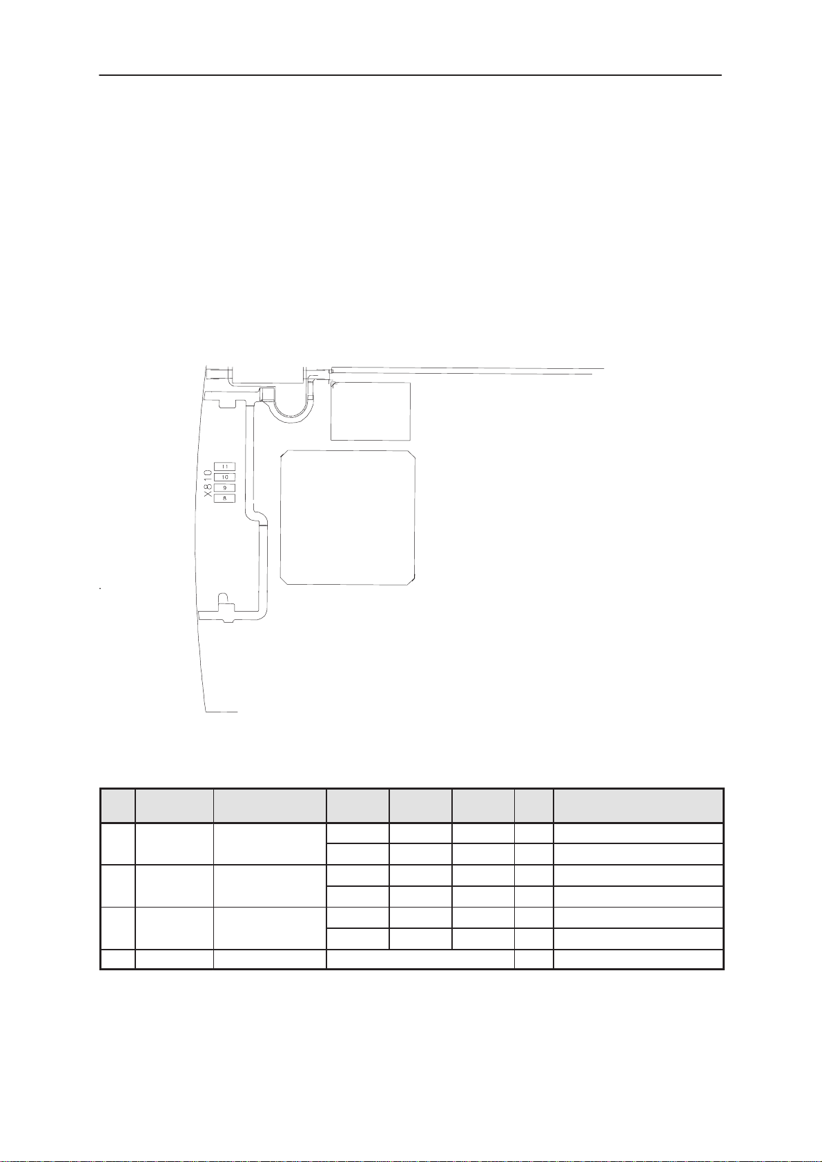
System connector X810
GND
X830
BS8
Page 5 – 6
Section 02/99
Page 7

PAMS
1,2,3,4,5/
RAE–2
Technical Documentation
DC Characteristics
Table 2. Supply Voltages and Power Consumption
Pin /
Conn.
1,2,3,4,5/
X830
X830
E307 VBACK
E312 VSYS
Line Symbol Minimum Nominal Maximum Unit Notes
VBATT
BS1
3.0 3.6 4.1 VDC Battery voltage,
SW limit
900 mA Current
2.4 3.0 3.15 VDC Backup battery
voltage
0.4 0.5 0.7 mA Charge current
0.25 0.4 mA Quiescent current
in suspend mode
2.75 2.8 2.85 VDC System voltage
0.050 300 450 mA Current
E300 V17_OUT
7/X800 V17_i1
8/X800 V17_i2
9/X800 V17_i3
17.1 19.4 21.6 VDC LCD Biasing voltage, NOTE1
19.0 19.8 20.6 VDC LCD Biasing voltage, at +20C
2 5 mA Current
15.8 17.9 19.9 VDC LCD intermediate
voltage1
(12/13xV17_OUT
). NOTE1
17.5 18.3 19.0 VDC at +20C
4 mA Current
14.4 16.4 18.3 VDC LCD intermediate
voltage2
(1 1/13xV17_OUT
). NOTE1
16.1 16.8 17.4 VDC at +20C
4 mA Current
2.6 3.0 3.3 VDC LCD intermediate
voltage3
(2/13xV17_OUT).
Max range
10/X800 V17_i4
Section 02/99
2.9 3.0 3.2 VDC at +20C
4 mA Current
1.3 1.5 1.7 VDC LCD intermediate
voltage4
(1/13xV17_OUT).
NOTE1
1.4 1.5 1.6 VDC at +20C
4 mA Current
Page 5 – 7
Page 8
RAE–2
PAMS
BS1
Table 2. Supply Voltages and Power Consumption (continued)
Conn.
3/X800 V28_1
21/N450 V28_2
46/X830 V28_3
16/X830 VBB
NOTE : Complete temperature range
Technical Documentation
NotesUnitMaximumNominalMinimumLine SymbolPin /
2.70 2.80 2.85 VDC LCD Logic voltage
1 4 mA Current
2.70 2.8 2.85 VDC IrDA Logic voltage
2 4 mA Current
2.75 2.8 2.85 VDC MMC supply voltage
0.01 50 100 mA Current
2.75 2.8 2.85 VDC Base Band operating voltage
mA Current
AC Characteristics
Minimum Nominal Maximum Unit / Notes
External XT AL
CPU clock 33.18 MHz, Rise time
Memory bus clock 33.18 MHz, Rise time
Memory Controller clock 66.3552 MHz, Rise time
MMC clock during data 0.2592 8.294 Mhz, Rise time
MMC clock during identification
32.768 kHz
20 ppm, accuracy
1–2ns
2–3ns
1–2ns
2–3ns, NOTE1
259.2 kHz, Rise time 2–3ns
NOTE: Frequency is a multiple of 259.2kHz
External Signals and Connections
This section describes the external electrical connection and interface levels on BS1 module. The electrical interface specifications are collected
into tables that cover each connector and defined interface.
Table 3. List of Connectors and testpoints
Connector Name Code Notes
UI flex connector X800 CMT/PDA LCD– and Keyboard signals
Board to Board connector X830 CMT PDA interface
System connector pads X810
Page 5 – 8
Section 02/99
Page 9
PAMS
Whol
RAE–2
Technical Documentation
Table 3. List of Connectors and testpoints
(continued)
BS1
NotesCodeConnector Name
Audio connector pads E880, E881,
HF–speaker connection and earpiece connection
E850, E851
Backup battery holder X451
Testpads E300–E315 Testpads ”under” battery pack
Frame connector pads X840 Include manufacturing testpads. Is removed before
assembly
Testpoints J310,
Testpoints around the BS1 PCB.
J400–J404,
J430, J434,
J435,
J440 – J456,
J497 – J499,
J801, J803,
J804, J808,
J854, J880,
J881
UI flex connector
The Interface between the BS2 and BS1 modules comprises a 51–pin
flex connector. The connector includes supply voltage for the BS2 module, and required information signals. Signals from the BS8 module are
also carried via the flex connector.
Table 4. UI flex Connector X800
Pin I/O Name Function Min Nom Max Unit Description /
1 GND Global Ground
2 I LCD_TEMP PDA LCD Temperature
3 O V28_1 PDA LCD Logic voltage 2.70 2.80 2.85 VDC
4 O LCD_ON PDA LCD enable
5 O V17_OUT PDA LCD Biasing voltage 19.0 19.8 20.6 VDC Range at +20C.
6 GND Global Ground
7 O V17_i1
8 O V17_i2
9 O V17_i3 2.9 3.0 3.2 VDC
10 O V17_i4 1.4 1.5 1.6 VDC
11 GND Global Ground
PDA LCD Intermediate bias
voltage
0.2 0.9 2.5 VDC Voltage range
0.2 0.9 0.91 VDC At +25_C
2.30 2.8 2.85 VDC High
17.5 18.3 19.0 VDC
16.1 16.8 17.4 VDC
Note
throught the whole
temperature range.
0 0.4 VDC Low
Whole range can
be seen from
table2
Range at +20C.
e range can
be seen from
table2
Section 02/99
Page 5 – 9
Page 10
RAE–2
B
d
B
d
B
d
B
d
PAMS
BS1
Table 4. UI flex Connector X800
12 O FRM PDA LCD Frame pulse
13 O M PDA LCD AC Modulation
14 GND Global Ground
15 O LC PDA LCD Line pulse
16 GND Global Ground
17 O SCK PDA LCD bus clock
18 GND Global Ground
19 O LCDD0 PDA LCD Data signal
20 O LCDD1 PDA LCD Data signal
21 GND Global Ground
22 O LCDD2 PDA LCD Data signal
23 O LCDD3 PDA LCD Data signal
24 O PDA_BL_ON PDA LCD Backlight enabled
25 O CMT_BL_ON CMT Backlight enabled
26 I ROW3 CMT Keys Row3, Lid closed,
ase band powere
27 I ROW2 CMT Keys Row2, Lid closed,
ase band powere
28 I ROW1 CMT Keys Row1, Lid closed,
ase band powere
29 I ROW0 CMT Keys Row0, Lid closed,
ase band powere
30 O COL4 CMT Keys Col4
31 O COL3 CMT Keys Col3
Technical Documentation
(continued)
Description /
UnitMaxNomMinFunctionNameI/OPin
Note
2.30 2.80 2.85 VDC High
0 0.45 VDC Low
72 100 Hz
% Duty cycle
2.30 2.80 2.85 VDC High
0 0.45 VDC Low
2.5 3.4 kHz
2.30 2.80 2.85 VDC High
0 0.45 VDC Low
32 44.5 kHz
2.30 2.80 2.85 VDC High
0 0.45 VDC Low
2.3 3.2 MHz
2.30 2.80 2.85 VDC High
0 0.45 VDC Low
2.30 2.80 2.85 VDC High
0 0.45 VDC Low
2.30 2.80 2.85 VDC High
0 0.45 VDC Low
2.30 2.80 2.85 VDC High
0 0.45 VDC Low
2.30 2.80 2.85 VDC High, backlight en-
0 0.45 VDC Low
2.1 2.80 2.85 VDC High, backlight en-
0 0.5 VDC Low
2.1 2.80 2.85 VDC High
0 0.5 VDC Low
2.1 2.80 2.85 VDC High
0 0.5 VDC Low
2.1 2.80 2.85 VDC High
0 0.5 VDC Low
2.1 2.80 2.85 VDC High
0 0.5 VDC Low
2.1 2.80 2.85 VDC High
0 0.5 VDC Low
2.1 2.80 2.85 VDC High
0 0.5 VDC Low
abled
abled
Page 5 – 10
Section 02/99
Page 11

PAMS
d
PDA
RAE–2
Technical Documentation
Table 4. UI flex Connector X800
32 O COL2 CMT Keys Col2
33 O COL1 CMT Keys Col1
34 O COL0 CMT Keys Col0
35 I APP_ROW1 PDA Application row1
36 I APP_ROW0 PDA Application row0
37 O APP_COL3 PDA Application col3
38 O APP_COL2 PDA Application col2
39 O APP_COL1 PDA Application col1
40 O APP_COL0 PDA Application col0
41 O LCDCD CMT LCD driver command/
ata selection
42 O LCDSCx CMT LCD driver chip select
43 GND Global Ground
44 O GENSCLK CMT LCD driver bus clock
45 GND Global Ground
46 O GENSDIO CMT LCD driver serial data
47 GND Global Ground
48 O LCDRST CMT LCD Reset
49 VBB 2.7 2.8 2.85 VDC
50 I PWRKEY CMT Power switch
51 VPDA Filtered battery voltage from
2.1 2.80 2.85 VDC High
2.1 2.80 2.85 VDC High
2.1 2.80 2.8 VDC High
2.0 2.80 2.85 VDC High
2.0 2.80 2.85 VDC High
2.3 2.80 2.85 VDC High
2.3 2.80 2.85 VDC High
2.3 2.80 2.85 VDC High
2.3 2.80 2.85 VDC High
2.1 2.80 2.85 VDC High, data
2.1 2.80 2.85 VDC High
2.1 2.80 2.85 VDC High
2.1 2.80 2.85 VDC High
2.1 2.80 2.85 VDC High
2.1 2.80 2.85 VDC Inactive state
3.0 3.6 4.1 V
40 65 mA PDA LCD back-
10 20 mA PDA LCD back-
(continued)
0 0.5 VDC Low
0 0.5 VDC Low
0 0.5 VDC Low
0 0.8 VDC Low
0 0.8 VDC Low
0 0.45 VDC Low
0 0.45 VDC Low
0 0.45 VDC Low
0 0.45 VDC Low
0 0.5 VDC Low, command
0 0.5 VDC Low, chip selected
0 0.5 VDC Low
4.0 MHz
0 0.5 VDC Low
4.0 MHz
0 0.5 VDC Low
0 0.45 VDC L(Pulse)=Power
0 mA PDA and CMT
UnitMaxNomMinFunctionNameI/OPin
BS1
Description /
Note
on/off, min 64ms
backlights off
light ON
light OFF
Section 02/99
Page 5 – 11
Page 12

RAE–2
(SRS)
PAMS
BS1
Technical Documentation
Board to board connector signals
All interfaces from the BS8 module to the BS1 module are fed over a
50–pin board-to-board connector.
The function of the Interface is to transfer the battery voltage from the
BS8 module, and transfer data between the BS8, BS2, and BS1 modules.
The signal definition and the most significant specifications of signals are
collected in the next table.
Table 5. Board to board connector X830
Pin I/O Name Function Min Nom Max Unit Description /
1
2
3
4
5
6 I XEAR Audio Output for Handsfree
VBATT Battery Positive
and Car Kit Use
3.0 3.6 4.1 V Unregulated Bat-
0.3 1000 mA Current from BS8
Note
tery Voltage
module
500 mVpp
7 GND Global Ground Reference for oth-
8 I BATTDET Battery Position Information
9 I HFENA Internal Handsfree Amplifier
Control
10 EARP Earpiece Positive
11 EARN Earpiece Negative
12 GND Global Ground
13 O PWRONx PDA start baseband to ser-
vice Request State
14 O 32kHz Sleep clock for the CMT
15 GND Global Ground
16 VBB CMT System Power
17 O PWRKEYx CMT Power Switch
2.0 2.80 2.85 VDC
0 0 0.8 VDC
2.1 2.80 2.85 VDC High, HF amplifier
0 0.5 VDC Low, HF amplifier
50 223 mVpp Differential signal
2.30 2.8 2.85 VDC High
0 0.45 VDC Low , powering up
2.30 2.8 2.85 VDC high
0 0.45 VDC low
12 mA Maximum current
32768 Hz Pulse frequency
20 50 80 % Duty cycle
1 % Jitter
2.7 2.8 2.85 VDC Regulated CMT
1 mA Maximum current
2.0 2.80 2.85 VDC Inactive state
0 0.45 VDC L(Pulse)=Power
er signals
enabled
disabled
the CMT
for PDA
baseband voltage
on/off, min. 64ms
Page 5 – 12
Section 02/99
Page 13

PAMS
Sel
Clock
D
RAE–2
Technical Documentation
Table 5. Board to board connector X830
18 I CMT_BL_ON CMT UI Light On
19 O ROW3 CMT Keys Row 3
20 O ROW2 CMT Keys Row 2
21 O ROW1 CMT Keys Row 1
22 O ROW0 CMT Keys Row 0
23 GND Global Ground
24 I COL4 CMT Keys Column 4
25 I COL3 CMT Keys Column 3
26 I COL2 CMT Keys Column 2
27 I COL1 CMT Keys Column 1
28 I COL0 CMT Keys Column 0
29 GND Global Ground
30 I LCDCD CMT LCD Command / Data
ect
31 I LCDRSTx CMT LCD Reset
32 I LCDCSx CMT LCD Chip Select
33 GND Global Ground
34 I GENSCLK CMT LCD and CCONT Serial
35 I GENSDIO CMT LCD and CCONT Serial
ata
36 GND Global Ground
37 O FBUS_RXD Fast Serial Data to CMT
38 I FBUS_TXD Fast Serial Data to PDA
BS1
(continued)
Description /
UnitMaxNomMinFunctionNameI/OPin
Note
2.1 2.8 2.85 VDC High, backlight en-
0 0.5 VDC Low
2.5 2.8 2.85 VDC High
0 0.2 VDC Low
2.5 2.8 2.85 VDC High
0 0.2 VDC Low
2.5 2.8 2.85 VDC High
0 0.2 VDC Low
2.5 2.8 2.85 VDC High
0 0.2 VDC Low
2.1 2.80 2.85 VDC High
0 0.5 VDC Low
2.1 2.80 2.85 VDC High
0 0.5 VDC Low
2.1 2.80 2.85 VDC High
0 0.5 VDC Low
2.1 2.80 2.85 VDC High
0 0.5 VDC Low
2.1 2.80 2.85 VDC High
0 0.5 VDC Low
2.1 2.80 2.85 VDC High, data
0 0.5 VDC Low, command
2.1 2.80 2.85 VDC High
0 0.5 VDC Low, LCD reset
2.1 2.80 2.85 VDC High
0 0.5 VDC Low, chip selected
2.1 2.80 2.85 VDC High
0 0.5 VDC Low
3.250 MHz Pulse frequency in
2.1 2.80 2.85 VDC High
0 0.5 VDC Low
1.625 MHz Maximum pulse
2.30 2.80 2.85 VDC High
0 0.45 VDC Low
2.1 2.80 2.85 VDC High
0 0.5 VDC Low
abled
active state
frequency
Section 02/99
Page 5 – 13
Page 14
RAE–2
PAMS
BS1
Table 5. Board to board connector X830
39 GND Global Ground
40 I/O MBUS Bidirectional Serial Bus
41 VSYS PDA System voltage
42 O LIDSWITCH Lid State Information
43 I MMC_SWITCH MMC Cover State Information
44 GND Global ground
45 I/O MMC_CMD MMC Command / Address /
Response, Bidirectional
46 MMC_VSYS MMC Power Supply
47 I/O MMC_DATA MMC Bidirectional Data
48 GND Global ground
Technical Documentation
(continued)
Description /
UnitMaxNomMinFunctionNameI/OPin
Note
2.30 2.80 2.85 VDC High, to the CMT
0 0.45 VDC Low, to the CMT
2.1 2.80 2.85 VDC High, from the
0 0.5 VDC Low, from the CMT
2.75 2.80 2.85 VDC
2 mA
2.75 2.80 2.85 VDC High, Cover open
0 VDC Low, Cover closed
10 kohm. Pull–up resistor
2.75 2.80 2.85 VDC High, Cover open
0 VDC Low, Cover closed
2.30 2.80 2.85 VDC Data to the card
0 0.45 VDC Data to the Card
2.1 2.80 2.85 VDC data from the card
0.34 VDC Data from the card
259.3 kHz frequency
2.75 2.85 VDC
0.01 100 mA Current
2.30 2.80 2.85 VDC Data to the Card
0 0.45 VDC Data to the card
2.1 2.80 2.85 VDC Data from the
0 0.34 VDC Data from the card
8.294 MHz frequency
CMT
High, Pulled up
with 10kohm resistor to MMC_VSYS
in CMT Module
Low
High, Pulled up
with 10kohm resistor to MMC_VSYS
in CMT Module
Low
High, Pulled up
with 10kohm resistor to MMC_VSYS
in CMT Module
Low
Card High, Pulled
up with 10kohm
resistor to
MMC_VSYS in
CMT Module
Low
Page 5 – 14
Section 02/99
Page 15

PAMS
RAE–2
Technical Documentation
Table 5. Board to board connector X830
49 O MMC_CLK MMC Clock
50 GND Global Ground
(continued)
Description /
UnitMaxNomMinFunctionNameI/OPin
Note
2.30 2.80 2.85 VDC High
0 0.45 VDC Low
0.2592 8.294 MHz Frequency
BS1
Section 02/99
Page 5 – 15
Page 16
RAE–2
d
d
PAMS
BS1
System connector pads
The RAE–2 System connector is a multipurpose connector, which is
shared with the BS8 module. In this section are described only the signals that are connected to the BS1 module. These signals are needed for
PC–connectivity. The connector comprises spring type contacts to the
BS1 and BS8 module. The PCB comprises pads on which the springs
are pressed.
Technical Documentation
Table 6. System Connector pads X810
Pin Line
10 DCE_DTR PDA CPU Data set
11 GND Global ground
Symbol
8 DCT_TX PDA CPU Receive
9 DCE_RX PDA CPU Transmit
Page 5 – 16
Parameter Minimum Nominal Maximum Unit Unit / Notes
ata
ata
ready
2.0 2.80 2.85 VDC
0 0.8 VDC
2.30 2.80 2.85 VDC
0 0.45 VDC
2.0 2.80 2.85 VDC
0 0.8 VDC
Section 02/99
Page 17

PAMS
RAE–2
Technical Documentation
Audio connector pads
The audio connector has two contact types. The earpiece contacts are of
spring type, and the contacts for the handsfree speaker are elastomeric
contacts.
Table 7. Audio connector pads
Pin Line
Symbol
E850 EARP Earpiece positive
E851 EARN Earpiece negative
E880 PHFEARN Handsfree speaker
E881 PHFEARP Handsfree speaker
Parameter Minimum Nominal Maximum Unit Unit / Notes
node
node
negative node
positive node
BS1
50 223 mVpp Differential voltage between
EARP and EARN nodes
6.0 Vpp VBATT=4.4V. Differential voltage between PHFEARN and
PHFEARP nodes
4.4 Vpp VBATT=3.6V. Differential voltage between PHFEARN and
PHFEARP nodes
6.0 Vpp VBATT=4.4V. Differential voltage between PHFEARN and
PHFEARP nodes
4.4 Vpp VBATT=3.6VBATT=4.4V. Differential voltage between
PHFEARN and PHFEARP
nodes.
Backup battery
Figure 2. Backup battery insertion direction
NOTE: Positive node is against PCB, it can be identified by 2mm diameter contact plate
Table 8. Backup battery holder X450
Pin Name Function Min Nom Max Unit Description / Note
VBACK Backup battery voltage 2.4 3.0 3.1 VDC
GND Global ground
Section 02/99
Page 5 – 17
Page 18

RAE–2
PAMS
BS1
Internal Signals and Connections
Table 9. IR–transceiver (N300) signals
Pin Line
Symbol
3 TXD Transmit data from CPU
4 RXD Receive data to CPU
Table 10. Signals between PDA CPU and Flash memories
Name Function Min Nom Max Unit Description / Note
SA(21:1) System address
SD(15:0) System data from CPU
ROMCS(2:0) Chip selects for Flash memo-
FLSHWRx Flash write signal
ROMRDx Flash read signal
GPIO_CS1 Write protect for RFD memory
GPIO_CS7 RFD Flash ready
Parameter Minimum Nominal Maximum Unit / Notes
2.30V 2.80V 2.85V
0V 0.45V
2.0V 2.8V 2.85V
0 0.8V
2.30 2.80 2.85 VDC High
2.30 2.8 2.85 VDC High
System data from memory
ries
2.40 2.8 2.85 VDC High
2.30 2.80 2.85 VDC High
2.30 2.80 2.85 VDC High
2.30 2.80 2.85 VDC High
2.30 2.80 2.85 VDC High
2.0 2.80 2.85 VDC High, ready
Technical Documentation
0 0.4 VDC Low
0 0.4 VDC Low
0 0.4 VDC Low
0 0.4 VDC Low
0 0.4 VDC Low, write enabled
0 0.4 VDC Low, read enabled
0 0.4 VDC Low, powered down
0 0.8 VDC Low, busy
Table 11. Signals between PDA CPU and DRAM Memory
Name Function Min Nom Max Unit Description / Note
MA(11:0) Memory address
SD(15:0) Memory data from CPU
Memory data from memory
RAS0 Row access strobe
CAS(1:0) Column access strobe
MWEx Memory write enable
2.30 2.80 2.85 VDC High
0 0.4 VDC Low
2.30 2.8 2.85 VDC High
0 0 0.4 VDC Low
2.0 2.8 2.85 VDC High
0 0 0.6 VDC Low
2.30 2.80 2.85 VDC High
0 0.4 VDC Low
2.30 2.80 2.85 VDC High
0 0.4 VDC Low
2.30 2.80 2.85 VDC High
0 0.4 VDC Low, write enabled
Page 5 – 18
Section 02/99
Page 19

PAMS
RAE–2
Technical Documentation
Table 12. Signals between PDA CPU and PWRU
Name Function Min Nom Max Unit Description / Note
SA(2:0) System address
SD(6:0) System data
CS3x Chip select for Phaser
IOWx Phaser write signal
IORx Phaser read signal
RESETx Reset for CPU, and for Flash
memories.
VBACK Back–up battery voltage 2.40 3.0 3.1 VDC High
V17_EN LCD bias voltage enable
V28_1EN LCD logic voltage enable
2.30 2.80 2.85 VDC High
0 0.4 VDC Low
2.40 2.8 2.85 VDC High
0 0.4 VDC Low
2.30 2.80 2.85 VDC High
0 0.4 VDC Low
2.30 2.80 2.85 VDC High
0 0.4 VDC Low, write enabled
2.30 2.80 2.85 VDC High
0 0.4 VDC Low, read enabled
2.30 2.80 2.85 VDC High
0 0.4 VDC Low
2.30 2.80 2.85 VDC High
0 0.4 VDC Low
2.30 2.80 2.85 VDC High
0 0.4 VDC Low
BS1
Section 02/99
Page 5 – 19
Page 20
RAE–2
PAMS
BS1
Functional Description
Power Unit
V17
V28_1
MMC V28_3
IrDA
HF–
power amp.
V28_2
VPDA
VPDA
VBATT
V28_1
PWRU
V28
VPDA VPDA
Interm.voltages 1–4
PWRGOOD
PWRGOOD
Charging
VBB
IOW
IOR
ADD(2:0)
DATA (6:0)
CS3x
V28_EN
V17_EN
RESETx
VBACK
BS2
TESTPADS
VSYS
Am486 CPU
PMI
NMI
PMI
Technical Documentation
BS1
VSYS
DRAM
VSYS
XIP
XIP
Write protect
NMI
Flashes
RESETx
VSYS
VPP
RESETx
RFD
RFD
Flash
VPP
FRAME CONNECTOR
Backupbattery
Lid Switch
VBATT
VSYS
VBB
BATTDET
MMC_SWITCH
BS8
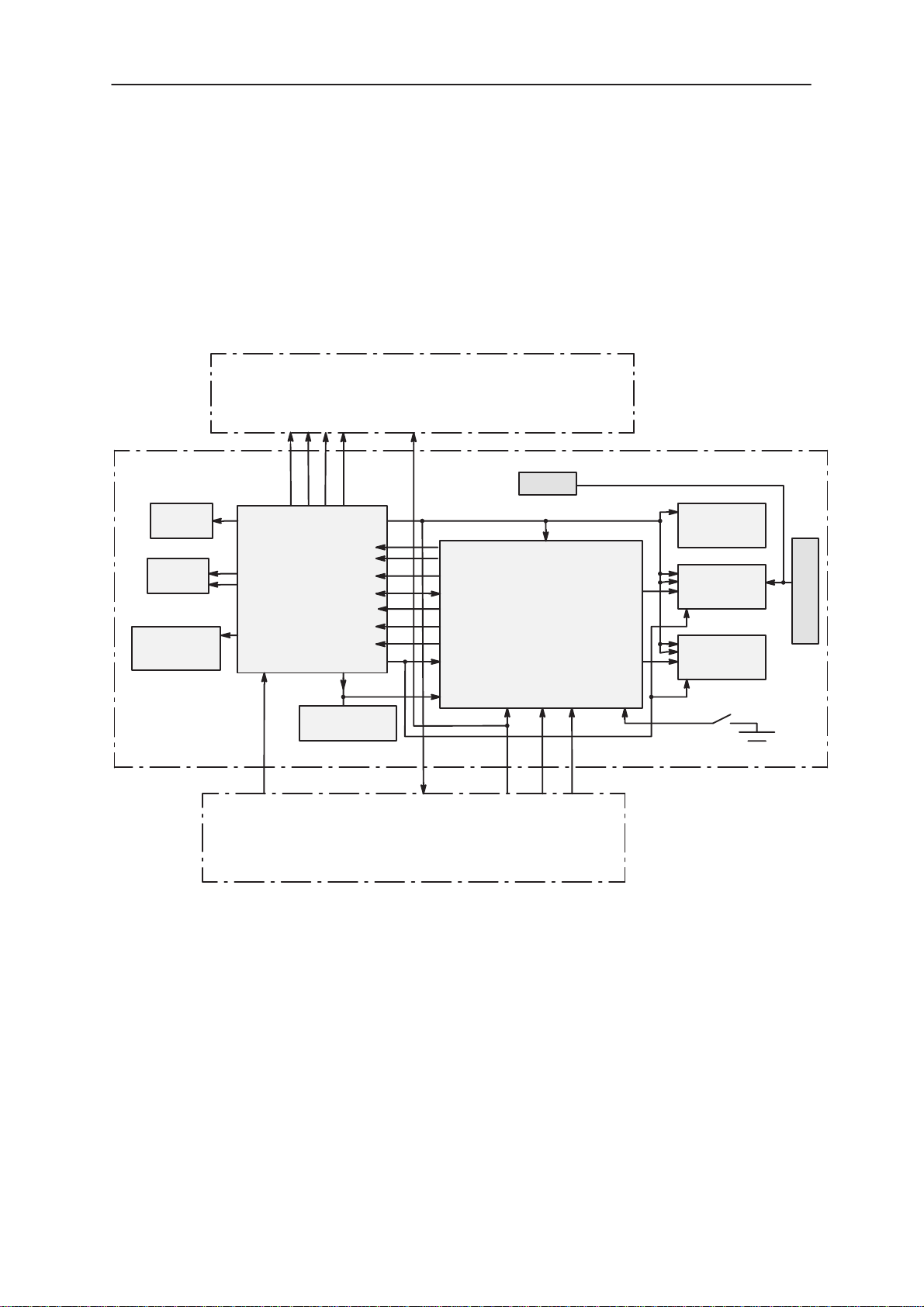
Figure 3. PDA Power distribution diagram
Battery voltage is supplied from the BS8 module through a board to board
connector. In the BS1 module the battery voltage is filtered and then supplied to the Phaser, IR–transceiver circuit, BS2 module, and PHF–speaker circuitry.
The phaser generates internally the system voltage V28, switched voltages V28_1 ,V28_2, V28_3, the LCD bias voltage V17, the LCD intermediate voltages V17_ix, x=1–4 and the backup battery charging voltage
VBACK.
When the battery voltage level is adequate, the PWRU switches V28 on
and after a certain time releases the reset–signal for the CPU. The CPU
Page 5 – 20
Section 02/99
Page 21

PAMS
RAE–2
Technical Documentation
controls the LCD, MMC, and IR–transceiver logic voltages by writing command to the PWRU register. Optionally the CPU can control the LCD logic- and biasing voltage directly by means of I/O signals.
The backup battery supplies power to the CPU’s real time clock. The
PWRU charges the backup battery when the main battery is connected.
The CPU puts the Flash memories to power down mode when they are
not used.
The BS8 signal BATTDET is a warning signal that the battery will be removed soon, when power down procedure is started. VBB is the supply
voltage for the CMT display, located in the BS2 module, and the VBB
provides information for the BS1 CPU whether the CMT powered or not
and it enables the keyboard buffer. The MMC_SWITCH indicates that the
MMC card will be removed, when the CPU controls the Phaser to turn the
V28_3 off.
Input filter
BS1
The Battery voltage is fed from the BS8 module and then filtered by using
a LC–lowpass filter, after filtering the voltage is named VPDA. The VPDA
is then fed to the PWRU, the IR–transceiver, the PHF–speaker circuitry,
and to the BS2 module.
Linear regulator V28
System voltage V28 is generated by a linear regulator. V28 stays on all
the time when the battery voltage is higher than cutoff limit.
Linear regulator V28_1,_2,_3
These regulators are controlled by the CPU. The CPU can enable these
regulators by writing a command to the PWRU’s register. V28_1 is the
switched V28 and is used for the LCD logic. V28_2 is the switched V28
and is used for the IRDA logic. V28_3 is the MMC voltage.
Switchmode regulator V17
The LCD bias voltage V17 is generated by a step–up DC–DC converter.
The control scheme is the current limited pulse width modulation (PWM).
The switching transistor is internal. The regulator output, too, is separated from the battery line by an integrated switch transistor between the
regulator output and load.
Backup battery
The Real time clock is kept running by a backup battery only when the
main battery is not connected. At the nominal RTC load used , the
12mAh capacity of the backup battery provides about 40 days of RTC operation when the main battery is not connected. The backup battery is
Section 02/99
Page 5 – 21
Page 22

RAE–2
PAMS
BS1
rechargeable. It is charged by the Phaser VBACK regulator using 0.5mA
current when the main battery is connected.
Reset and power management
The Phaser is connected to the I/O space of the H3 by using a 7 bit wide
data bus and a 3 bit wide address bus. The BS2 PDAPWRU on the PDA
board supplies two different voltage levels to the system;
2.85V is used as the main operating voltage for all circuits and
about 19V that is needed for the LCD bias (V17). The LCD bias voltage is
used to adjust the contrast ratio of the LCD screen. The LCD bias voltage is controlled by the Phaser ASIC.
The V17 and V28_1 ON/OFF are switched by the Phaser, but optionally
also the CPU can control these signals directly with HW means, independently of the SW controlled register settings. The phaser provides also
the POWERGOOD signal for the CPU. The system reset circuit is part of
the power supply. When the battery voltage is higher than 3.4V a
PWRGOOD is generated for the CPU. The reset circuit also asserts the
reset signal whenever the Vcc supply voltage declines below the threshold, keeping it asserted for at least 50ms after Vcc has risen above the
reset threshold. The reset circuit is designed to ignore fast transients
(t < 64µs) in Vcc.
Technical Documentation
There is an undervoltage lockout (UVLO) block inside the Phaser. Below
the threshold limit the comparator shuts down all Phaser functionality to
prevent the battery from overdischarge. Otherwise the VSYS regulator
current drains the battery when left unused for long period. After the
UVLO there is only reference block in the Phaser drawing current from
the battery. The UVLO has a little hysteresis and is cancelled when the
battery voltage has risen to 2.7V. However, reset to the CPU is given only
when battery voltage rises to 3.45V. This in order to avoid unsuccessful
power–ups. When the lockout voltage level is reached, the battery voltage rises because the load is removed.
PDA CPU
The PDA CPU is a SC450–33CC in a 256 pin plastic ball grid array package.
The core features a 32–bit architecture with internal 8k write–back cache.
The clock rate is 33MHz, which can be slowed down to1MHz. The default clock rate on reset is 8.29MHz. The bus clock rate is 33MHz. A
32kHz clock signal for the BS8 module is provided by the CPU PLL circuit. The clock signal is started when ever the system voltage is applied
to the CPU.
The CORE starts when the reset signal is provided and then it begins to
execute the program code from the Flash memory. The external pull–up
resistor controls the start–up procedure (Boot code Chip select, and data
bus width).
Page 5 – 22
Section 02/99
Page 23

PAMS
RAE–2
Technical Documentation
The memory controllers are integrated to the chip. A ROM controller is
used for Flash interface and a DRAM controller supports extended data
out (EDO) page mode DRAMs. Both memory types (DRAM and Flash)
have their own address and data bus routed directly to the CPU. The
power unit is controlled via an I/O-mapped 7-bit wide data- and 3-bit wide
address bus, which is shared with Flash data- and address bus. The CPU
block diagram is the figure below.
Am486SLE
Core
DMA
controller
8237
Reset
Loop filters
x32kHz
32kHz xtal
Power
management
unit
Clock
generation
Real time
clock
Addr
Data
Addr
Memory
management
unit
Address
decoder
Data
steering
Graphics
controller
MMC bus
controller
BS1
SA bus
Data bus
LCD
MMC bus
JTAG port
GPIO’s
Boundary
scan
AT port
logic
Timer
8254
Interrupt
controller
8259
Memory
controller
Keyboard cntrl
matrix/XT
UART
16550
UART
16550
Elan SC450–33CC
DRAM control
ROM control
IrDA
infrared
controller
Columns
Rows
FBUS
Serial port
R–tranceiver
For serial interface two UART circuits are used. UART2 is a serial interface reserved for data transfer between the BS1 and BS8 modules.
UART2 is disabled or enabled according to the CMT voltage. UART1 is
used for RS–232 interface with external level changer. The UARTs can be
connected together to establish Re–Link connection, where received data
is directly linked to the UART’s transmit data pin. That way the BS8 module can be programmed by using an external RS-interface. Autobauding
detection circuitry is included in the UART1 block.
Section 02/99
Page 5 – 23
Page 24

RAE–2
PAMS
BS1
Technical Documentation
The LCD–controller supports a 4-bit data and 16-grey shades. The display control signals are routed from the CPU. The bigger (640x200) LCD
is located in the lid. The interconnection between the CPU and the LCD
comprises a flex through the hinge. Data and control signals are provided
by the CPU. The required voltages are supplied by the PWRU.
The PDA CPU supports a synchronous serial interface that is compatible
with the Multimedia Card Bus (MMC) Protocol. The MMC is changeable
Flash or ROM memory card with variable memory size. The MMC connector is located on the BS8 Module. MMC signals are routed to the BS8
module through a Board to board connector. The interface consists of
three pins: one clock(output), one command/response (bidirectional), and
one data pin (bidirectional). The controller is capable up to 8Mbits/second
transfer rate.
The keyboard controller includes a matrix keyboard which is used for
PDA keyboard and for PDA lid keys. The PC/AT standard core includes
a 8254 programmable interval timer, two 8259 programmable interrupt
controllers, and a real time clock. The CPU’s general purpose input/outputs (GPIO) are controlled by the CPU’s registers.
I/O Signals
In the Table 13 below are listed BS1 module I/O signals which are
mapped to general purpose pins of the CPU.
Table 13. Spock CPU Controllable I/O Signals
Scotty Pin Signal Name Low High Note
GPIO_CS1 RFD_WPx Write operation Write not possible
GPIO_CS2 XIP_STS Memory busy Memory ready Input, CS(1:0) Flash memory status
GPIO_CS5 TESTMODEx Testmode acti-
vated
GPIO_CS6 PWRONx Powering the
CMT up
GPIO_CS7 Flash_RDY Flash performing
an internal operation
GPIO_CS8 MMC_Switch MMC cover
closed
GPIO_CS9 MBUS Output during BS8 Flashing from BS1
GPIO_CS11 Phaser_CSx Chip Selected Chip not selected Output.
GPIO_CS12 VBB CMT off Reset, CMT on Input.
GPIO_CS13
GPIO16 LCDBL_EN Reset, Suspend,
BL disabled
GPIO18 BZR_EN Reset, Suspend Operation Enables the PA.
BL1 BATTDET Battery con-
nected
SUS/RES LIDSWITCH Cover closed Cover open STI. Indicates when the coved is open
Reset, Suspend,
Operation
Reset, Suspend Activate the power on procedure for the
Flash ready for
new command
Reset, MMC cover open
Backlight activated
Battery removed Indicates when the battery is going to
Input.
CMT
Input. Open drain output, processor’s
internal pull–up is used. (Only for the
RFD)
Input. MMC cover status indication
module, Input otherwise.
Backlight EL driver controller.
be removed. Pin has build in 15ms debounce
or closed
Page 5 – 24
Section 02/99
Page 25

PAMS
RAE–2
Technical Documentation
Table 13. Spock CPU Controllable I/O Signals (continued)
LVDD LVDD Reset, Suspend PDA LCD Logic
LVEE LVEE Reset, Suspend PDA LCD bias
voltage activated
voltage activated
Memories
The memory units of the module are connected to the CPU via a 16–bit
wide data bus. Both memory types (DRAM and Flash) have an own
data– and address bus.
MD [15:0]
MA [11:0]
control [3:0]
DRAM
BS1
Routed to the Phaser
Routed to the Phaser
control [7:0]
BS1 CPU
SD [15:0]
SA [21:0]
DRAM memory
The 1Mx16bit DRAM is connected to the CPU with a dedicated 16–bit
wide data- and 12-bit wide address bus. The DRAM type used is the extended data out (EDO) DRAM with 60ns access time, and self–refresh
capability. DRAM is packaged in a 5.55mmX9.10mm, 40–ball uBGA
package.
XIP Flash 1RFD Flash XIP Flash 0
When the DRAM is driven by the CPU, no wait states is needed.
Flash memory
Three 1Mx16bit Flash memory devices are used for non–volatile memory.
The Flash type features a 120ns access time. The Flash is packaged in
8mmX11mm 64–ball CSP package. When the Flash is read by the CPU,
4 wait states are needed to ensure proper timing.
Section 02/99
Page 5 – 25
Page 26

RAE–2
PAMS
BS1
External Serial Interface
The UART1 External serial interface is used for PC–connectivity. The RS–
connection is provided by a 3–signal interface (RXD,TXD, and DTR)
which is routed to the system connector. Maximum data rate is
230.4kbps.
The re–link feature connects the UART1 and the UART2 (FBUS) internal-
ly together. This provides the signal routing from the system connector to
the CMT.
The Autobaud detection circuitry can detect bit rates from 300 bps tp
115.2kbps. The autobaud state machine starts when enabled by the CPU.
The bit rate measurement begins on the first negative edge of the
CPU_RXD line. After detecting the start bit width, and therefore the bit
rate, the remainder of the incoming data stream is sampled at this rate.
This UART is shared with the IrDA circuitry and thus only one of them can
be used at a time.
Technical Documentation
IR–Transceiver
The IR–transceiver controller is shared with the UART1. Infrared data
transfer is started with 9600bps and then the data rate is increased to
115.2kbps if the connected device supports higher speed. The protocol is
the standard one of the Infrared Data Association. The CPU hardware
implementation includes bit stuffing (when transmitting), CRC calculation,
removing bit stuffing, and removing beginning of frame (when receiving) .
Handsfree loudspeaker
The Handsfree speaker power amplifier circuitry is located on the BS1
module. The HF–speaker is used to produce the PDA key–click sounds,
error beeps, and tunes. When the lid is opened, the loudspeaker is used
as an handsfree speaker, producing key–click sound when a PDA
QWERTY key is pressed, and producing tunes. The HF–speaker power
amplifier can be controlled by the PDA CPU, or CMT.
Keyboard
The keyboard interface comprises 10x8 matrix lines. The QWERTY keyboard pads are located on the other side of the BS1 module board. 4x2
(2Row/4Column) matrix is routed to the lid. Four columns are multiplexed
with CMT keyboard columns. Multiplexing is done by using buffer located
on the BS1 module. This buffer is controlled by Baseband voltage (VBB).
When the lid is closed these four columns are switched to inputs and they
are not read by the CPU.
Page 5 – 26
Section 02/99
Page 27

PAMS
RAE–2
Technical Documentation
Table 14. Key Reference Numbers vs. Senses and Drives.
Col0 Col1 Col2 Col3 Col4 Col5 Col6 Col7
Row0 S730 S732 S734 S736 S331 S337 S343
Row1 S731 S733 S735 S325 S330 S336 S341 S342
Row2 S300 S318 S347 S324 S335 S31 1 S303 S305
Row3 S306 S307 S308 S327 S328 S310 S309 S323,
Row4 S312 S313 S314 S332 S333 S316 S315 S317
Row5 S301 S319 S320 S321 S322 S348 S349 S302
Row6 S352 S353 S354 S338 S339 S356 S355
Row7 S357 S358 S359 S344 S345 S361 S360 S346
Row8 S362 S363 S364 S326 S351 S365 S350
Row9 S304,
BS1
Column
S329,
S334
S340
NOTE1: Shift pads has dedicated Sense line (ROW9), These shift pads
are connected parallel
NOTE2: Grey shaded switches are located in BS2 module.
Figure 4. BS1 PDA keyboard
Section 02/99
Page 5 – 27
Page 28
RAE–2
PAMS
BS1
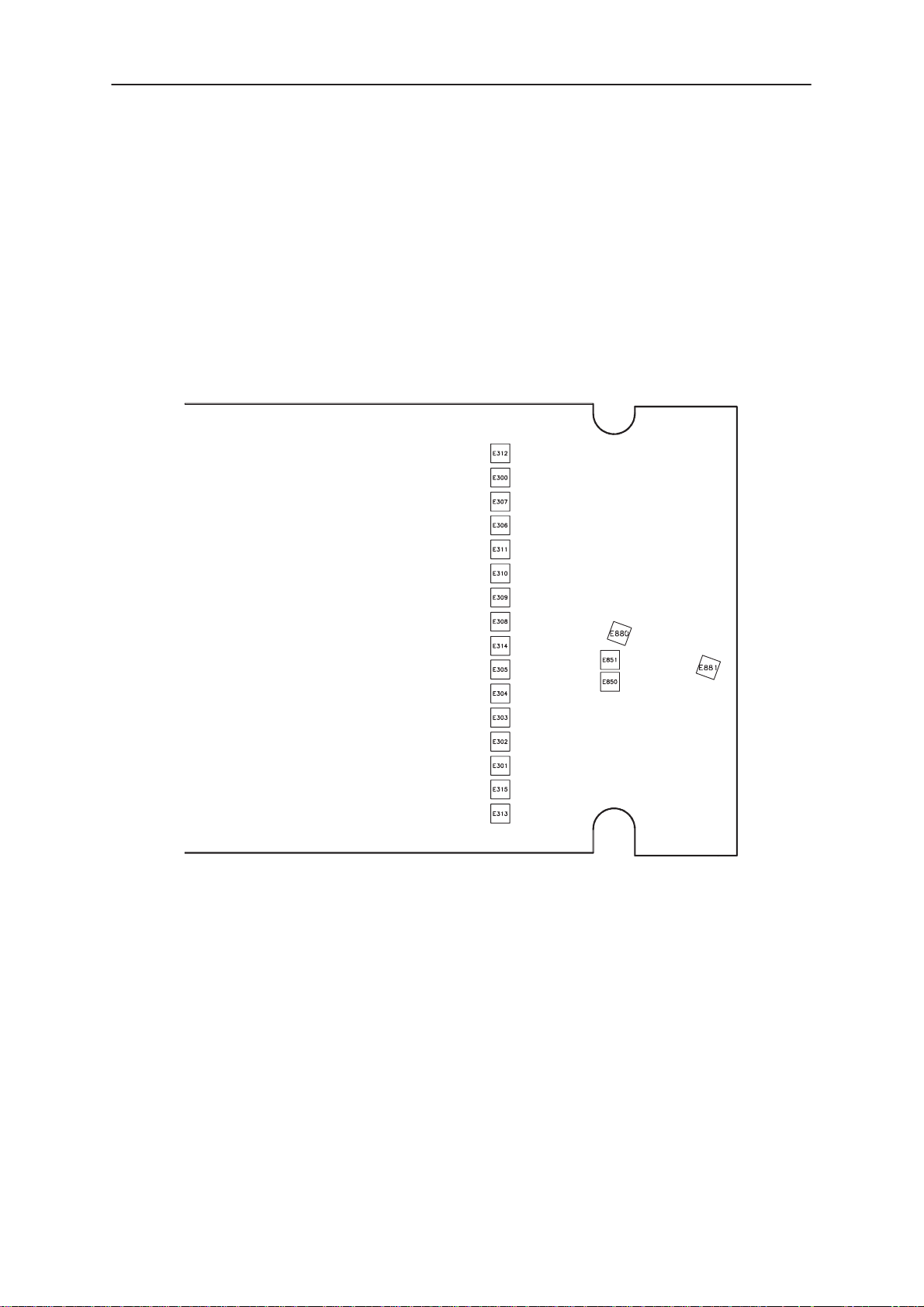
Test pads
Test pads are located under the battery pack. They include JTAG port
which is used for After Sales Flashing purposes. The different voltages
can be measured from these testpads. Serial data transfer test pads are
used for data transfer between the BS1 and BS8 modules.
Technical Documentation
Page 5 – 28
Figure 5. Test pad layout
Section 02/99
Page 29

PAMS
E310
RAE–2
Technical Documentation
Table 15. Test pads
Pin I/O Name Function Min Nom Max Unit Description /
E300 V17_OUT PDA LCD Biasing voltage
E301 I BNDSCN_TMS Boundary scan Test mode se-
E302 I BNDSCN_TCK Boundary scan test clock
E303 I BNDSCN_TDI Boundary scan data in
E304 O BNDSCN_TDO Boundary scan data out
E305 I BNDSCN_EN Boundary scan enabled
E306 I Flash VPP Flashing voltage for XIP
E307 VBACK Backup battery voltage 2.40 3.0 3.10 VDC High
E308 O FBUS_RXD PDA CPU Tx–pin
E309/
E311 I/O MBUS Bidirectional Serial Bus
E312 VSYS System voltage 2.75 2.80 2.85 VDC
E313 GND Global Ground
E314 I FLSHWRx Write signal for Flash memo-
E315 I TESTMODEx testmode activation
I FBUS_TXD1,2 PDA CPU Rx–pin
lect
Flashes.
ries
Note
13.8 19.4 22.2 VDC High
0 VDC Low
2.0 2.80 2.85 VDC High, test mode
selected
0 0.8 VDC Low
2.0 2.80 2.85 VDC High
0 0.8 VDC Low
2.0 2.80 2.85 VDC High
0 0.8 VDC Low
2.30 2.80 2.85 VDC High
0 0.45 VDC Low
2.0 2.80 2.85 VDC High, boundary
scan enabled
0 0.8 VDC Low
2.75 2.80 2.85 VDC Connected to
VBATT inside
the Service
battery.
2.30 2.80 2.85 VDC High
0 0.45 VDC Low
2.0 2.80 2.85 VDC High
0 0.8 VDC Low
2.30 2.80 2.85 VDC High, to the
CMT
0 0.45 VDC Low, to the
CMT
2.1 2.80 2.85 VDC High, from the
CMT
0 0.5 VDC Low, from the
CMT
2.30 2.80 2.85 VDC High
0 0.45 VDC Low, write en-
abled
2.0 2.80 2.85 VDC High
0 0.8 VDC Low, testmode
enabled
BS1
NOTE : Testpad E308 ... E310 is reserved for R&D use.
Section 02/99
Page 5 – 29
Page 30

RAE–2
PAMS
BS1
Testpoints
Testpoints are located around the PDA PCB. They include clock, control,
data signals and voltages which is used for R&D, fault finding and testing
purposes.
Technical Documentation
Figure 6. Testpoints layout
Table 16. Testpoints
Point I/O Name Function Min Nom Max Unit Description /
J310 LID_SWITCH_IF Lid switch state
J400 33MHz CPU core clock
J401 O X32_CLK CMT sleep clock
J402 I VBB CMT baseband voltage
2.75 2.8 2.85 VDC High, lid open
0 VDC Low, lid closed
2.3 2.80 2.85 VDC High
0 0.45 VDC Low
2.3 2.80 2.85 VDC High
0 0.45 VDC Low
2.7 2.80 2.85 VDC High
1.0 mA Maximum cur-
Note
rent
Page 5 – 30
Section 02/99
Page 31

PAMS
CPU
RAE–2
Technical Documentation
Table 16. Testpoints
J403 I/O MBUS Bidirectional Serial Bus
J404 O PWR_ONx
J430 LF_INT Intermidiate PLL loop filter 1.2 VDC When PLLs are
J434 I X32IN
J435 O X32OUT
J440 ROMCS2 RFD flash chip select
J441 ROMCS0 XIP1 flash chip select
J442 FLASHWRx XIP and RFD flashes write
enable from
I XIP and RFD flashes write
enable from frame connector
or testpads
J443 ROMRDx RFD flash read enable
J444 WP RFD flash write protect
J445 ROMCS1 XIP2 flash chip select
J446 RASx DRAM row address strobe
J447 MWEx DRAM write enable
J448 CASL1x DRAM upper column address
select
J449 CASL0x DRAM lower column address
select
J450 FLASH_CTRL2 RFD flash status
(continued)
UnitMaxNomMinFunctionNameI/OPoint
2.30 2.80 2.85 VDC High, to the
0 0.45 VDC Low, to the
2.1 2.80 2.85 VDC High, from the
0 0.5 VDC Low, from the
2.0 2.80 2.85 VDC High
0 0.45 VDC Low
1.35 VDC High, Sini vawe
0 VDC Low
1.0 VDC High
–0.3 VDC Low
2.3 2.80 2.85 VDC High
0 0.45 VDC Low, chip se-
2.3 2.80 2.85 VDC High
0 0.45 VDC Low, chip se-
2.3 2.80 2.85 VDC High
0 0.45 VDC Low, write en-
2.0 2.80 2.85 VDC High
0 0.8 VDC Low, write en-
2.3 2.80 2.85 VDC High
0 0.45 VDC Low, read en-
2.3 2.80 2.85 VDC High
0 0.45 VDC Low, write pro-
2.3 2.80 2.85 VDC High
0 0.45 VDC Low
2.3 2.80 2.85 VDC High
0 0.45 VDC Low
2.3 2.80 2.85 VDC High
0 0.45 VDC Low
2.3 2.80 2.85 VDC High
0 0.45 VDC Low
2.3 2.80 2.85 VDC High
0 0.45 VDC Low
2.4 2.80 2.85 VDC High
0 0.4 VDC Low
BS1
Description /
Note
CMT
CMT
CMT
CMT
locked
lected
lected
abled
abled
abled
tected
Section 02/99
Page 5 – 31
Page 32
RAE–2
d
PAMS
BS1
Table 16. Testpoints
J451 STS1 XIP1 flash status
J452 STS2 XIP2 flash status
J453 SD1 System data bus line 1
J454 SA4 System address bus line 4
J455 D0 Memory data bus line 0
J456 MA3 Memory address bus line 3
J497 VCOMP1 1.24 1.285 VDC
J498 CS3x Phaser chip select
J499 RESETx Reset from Phaser to CPU
and flash memories
J801 O GENSDIO CMT LCD and CCONT serial
ata
J803 I/O LCDCD CMT LCD command / data
select
J804 I/O LCDCSx CMT LCD chip select
J808 O SCK PDA LCD data clock 2.3 2.80 2.85 VDC High
J854 BZR_IF Buzzer signal
J880 HFENA Handsfree earpiece enable
J881 O XEAR Audio output for handsfree
use
(continued)
2.4 2.80 2.85 VDC High
2.4 2.80 2.85 VDC High
2.3 2.80 2.85 VDC High, data to
2.4 2.8 2.85 VDC High, data to
2.3 2.80 2.85 VDC High
2.3 2.80 2.85 VDC High
2.3 2.80 2.85 VDC High
2.3 2.80 2.85 VDC High
2.5 2.80 2.85 VDC High
2.0 2.80 2.85 VDC High
2.0 2.80 2.85 VDC High, data
2.1 2.80 2.85 VDC High
2.0 2.80 2.85 VDC High
2.3 2.80 2.85 VDC High, HF ampli-
Technical Documentation
UnitMaxNomMinFunctionNameI/OPoint
0 0.4 VDC Low
0 0.4 VDC Low
0 0.45 VDC Low, data to
0 0.4 VDC Low, data to
0 0.45 VDC Low
0 0.45 VDC Low
0 0.45 VDC Low
0 0.4 VDC Low, chip se-
0 0.5 VDC Low
0 0.5 VDC Low
0 0.6 VDC Low, command
0 0.5 VDC Low, chip se-
0 0.6 VDC Low
0 0.45 VDC Low, HF ampli-
2.0 Vpp
Description /
Note
memory
memory
CPU
CPU
lected
lected
fied enabled
fied disabled
Page 5 – 32
Section 02/99
 Loading...