

Page 1

PAMS Technical Documentation
RAE–2 Series
Chapter 7
Troubleshooting
Original 02/99
Copyright 1999. Nokia Mobile Phones. All Rights Reserved.
Page 2
RAE–2
PAMS
Troubleshooting
Amendment
Number
Date Inserted By Comments
02/99 Original
Technical Documentation
AMENDMENT RECORD SHEET
Page 7 – 2
Original 02/99
Page 3

PAMS
RAE–2
Technical Documentation
CONTENTS –Troubleshooting
Introduction 7 – 5. . . . . . . . . . . . . . . . . . . . . . . . . . . . . . . . . . . . . . . . . . . .
General 7 – 5. . . . . . . . . . . . . . . . . . . . . . . . . . . . . . . . . . . . . . . . . . . . . . . .
Current consumption 7 – 5. . . . . . . . . . . . . . . . . . . . . . . . . . . . . . . . . .
Finding faulty module 7 – 5. . . . . . . . . . . . . . . . . . . . . . . . . . . . . . . . .
CMT Troubleshooting 7 – 7. . . . . . . . . . . . . . . . . . . . . . . . . . . . . . . . . . .
Baseband faults 7 – 7. . . . . . . . . . . . . . . . . . . . . . . . . . . . . . . . . . . . . .
CMT is totally dead 7 – 8. . . . . . . . . . . . . . . . . . . . . . . . . . . . . . . . .
Power doesn’t stay on or phone is jammed 7 – 9. . . . . . . . . . . .
Display Information: Contact Service 7 – 10. . . . . . . . . . . . . . . . . .
The phone doesn’t register to the network... 7 – 10. . . . . . . . . . .
SIM card is out of order 7 – 13. . . . . . . . . . . . . . . . . . . . . . . . . . . . .
Audio fault 7 – 14. . . . . . . . . . . . . . . . . . . . . . . . . . . . . . . . . . . . . . . .
Charging fault 7 – 16. . . . . . . . . . . . . . . . . . . . . . . . . . . . . . . . . . . . .
Flash programming doesn’t work 7 – 17. . . . . . . . . . . . . . . . . . . . .
RF Fault 7 – 21. . . . . . . . . . . . . . . . . . . . . . . . . . . . . . . . . . . . . . . . . .
Required Servicing Equipment: 7 – 21. . . . . . . . . . . . . . . . . . . . . .
Test Points on BS8 Module 7 – 21. . . . . . . . . . . . . . . . . . . . . . . . . .
Transmitter fault 7 – 24. . . . . . . . . . . . . . . . . . . . . . . . . . . . . . . . . . . .
Receiver fault 7 – 26. . . . . . . . . . . . . . . . . . . . . . . . . . . . . . . . . . . . . .
AFC Fault 7 – 27. . . . . . . . . . . . . . . . . . . . . . . . . . . . . . . . . . . . . . . . .
1st IF 7 – 28. . . . . . . . . . . . . . . . . . . . . . . . . . . . . . . . . . . . . . . . . . . . .
2nd IF 7 – 29. . . . . . . . . . . . . . . . . . . . . . . . . . . . . . . . . . . . . . . . . . . .
UHF LO 7 – 30. . . . . . . . . . . . . . . . . . . . . . . . . . . . . . . . . . . . . . . . . . .
VHF LO 7 – 31. . . . . . . . . . . . . . . . . . . . . . . . . . . . . . . . . . . . . . . . . . .
Troubleshooting
Page No
PDA Troubleshooting and Service 7 – 32. . . . . . . . . . . . . . . . . . . . . . . . .
Required Servicing Equipment: 7 – 32. . . . . . . . . . . . . . . . . . . . . . . . .
Block Diagram 7 – 32. . . . . . . . . . . . . . . . . . . . . . . . . . . . . . . . . . . . . . .
BS1 PDA Components 7 – 34. . . . . . . . . . . . . . . . . . . . . . . . . . . . . . . .
BS1 Troubleshooting 7 – 35. . . . . . . . . . . . . . . . . . . . . . . . . . . . . . . . . .
Power–on malfunction 7 – 37. . . . . . . . . . . . . . . . . . . . . . . . . . . . . .
Power Circuitry Check 7 – 39. . . . . . . . . . . . . . . . . . . . . . . . . . . . . .
Troubleshooting Diagram of the PLL clock 7 – 40. . . . . . . . . . . .
Troubleshooting Diagram of the LCD 7 – 44. . . . . . . . . . . . . . . . .
Troubleshooting Diagram of the PDA LCD Backlight 7 – 45. . . .
Troubleshooting Diagram of the PDA Keyboard 7 – 46. . . . . . . .
Troubleshooting Diagram of the serial connections 7 – 47. . . . .
Troubleshooting Diagram of the IR connection 7 – 49. . . . . . . . .
Troubleshooting Diagram of the lid switch 7 – 50. . . . . . . . . . . . .
Troubleshooting Diagram of the HF Speaker 7 – 51. . . . . . . . . . .
Troubleshooting Diagram of the Earphone 7 – 52. . . . . . . . . . . . .
Original 02/99
Page 7 – 3
Page 4

RAE–2
PAMS
Troubleshooting
Troubleshooting Diagram of the Memory Card interface 7 – 53.
POST BEEP Codes 7 – 54. . . . . . . . . . . . . . . . . . . . . . . . . . . . . .
UI Troubleshooting 7 – 55. . . . . . . . . . . . . . . . . . . . . . . . . . . . . . . . . . . . . .
Mechanical Troubleshooting 7 – 55. . . . . . . . . . . . . . . . . . . . . . . . . . .
Keyboard Troubleshooting 7 – 55. . . . . . . . . . . . . . . . . . . . . . . . . . . . .
CMT LCD Module Troubleshooting 7 – 56. . . . . . . . . . . . . . . . . . . . .
PDA LCD Display Troubleshooting 7 – 59. . . . . . . . . . . . . . . . . . . . . .
CMT Backlighting Circuit Troubleshooting 7 – 63. . . . . . . . . . . . . . . .
PDA LCD Backlighting Circuit Troubleshooting 7 – 64. . . . . . . . . . .
Technical Documentation
Page 7 – 4
Original 02/99
Page 5
PAMS
RAE–2
Technical Documentation
Introduction
This document is intend to be a guide for localizing and repairing electrical faults in RAE–2 device. First there is short guide for fault localizing.
Then fault repairing is divided into three troubleshooting paths, each per
any module. Needed equipments are present before any actions.
Before any service operation you must be familiar with RAE–2 product
and module level architecture. You must also be familiar with RAE–2
specified service tools like the WinTesla service software, Flashing tools
and softwares. Basic skills of using RF measurement devices are required when you are starting to follow RF troubleshooting paths.
General
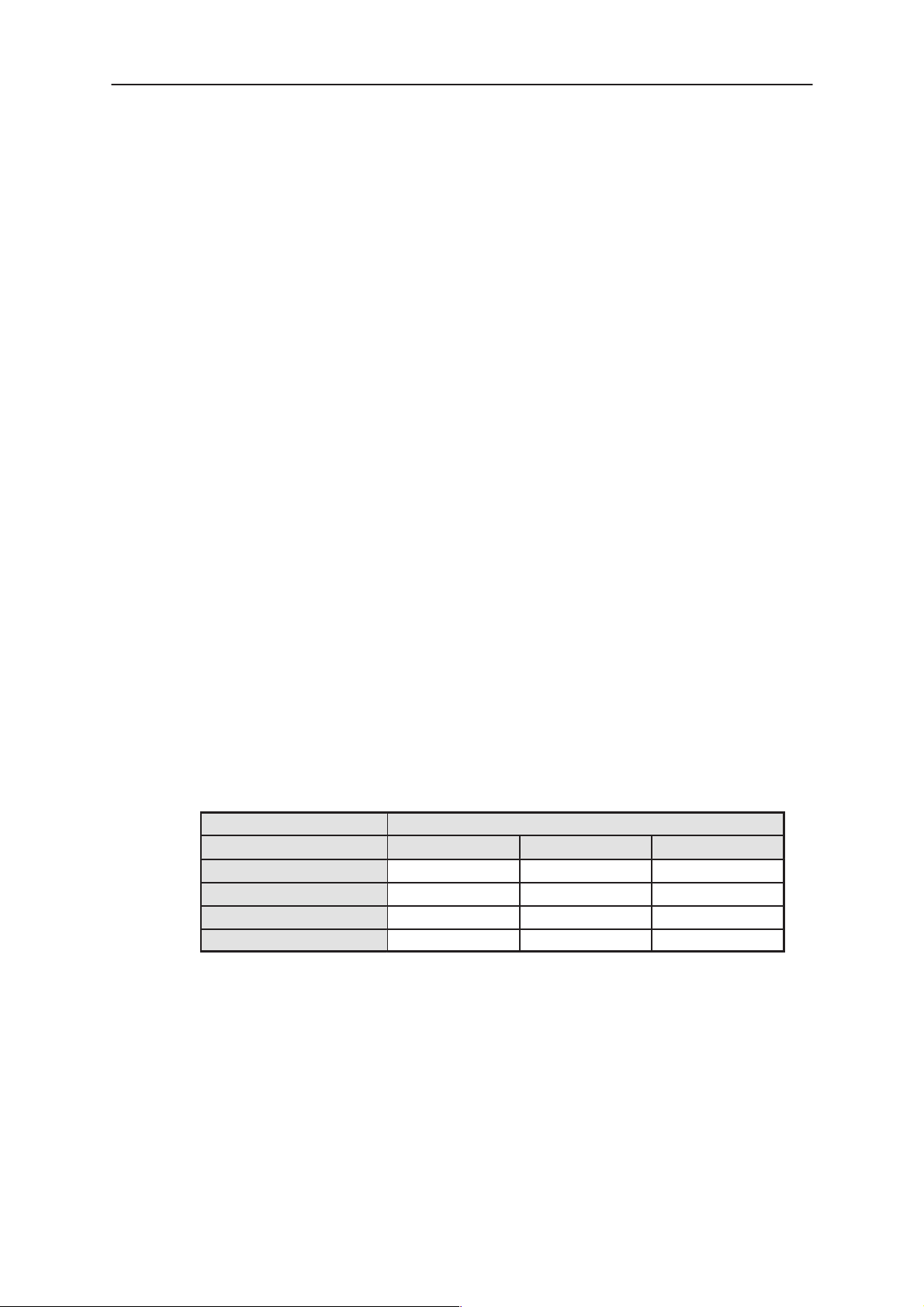
When you have a faulty RAE–2 device and you are starting troubleshooting it, check first the following basics.
Troubleshooting
–
Device hasn’t any mechanical damage.
– Device, especially connectors, are not dirty or moist.
– Screws are tightened as specificed.
– Battery voltage is high enough (nominal battery voltage is 3.6V).
– Current consumption is in normal area (this can be checked with Service Battery
BBS–5, if ReLink mode is disabled).
Current consumption
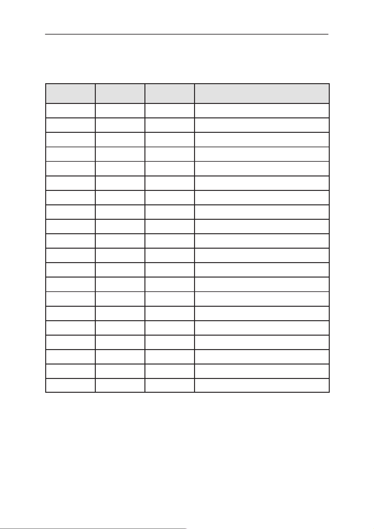
PDA mode (PDA current) Off (< 1.0mA) Idle (3–40mA) Call (140–320mA)
Active (200–380mA) 200–380mA 203–420mA 340mA–700mA
Standby (35–65mA) 35–45mA 38–85mA 175–365mA
Suspended (2–4mA) 2–3mA 5–43mA 142–323mA
Reset <1.0mA 3–40mA 140–320mA
Note1: CMT peak current consumption might be 5x more than is specified above.
Finding faulty module
CMT mode (CMT current)
Then you define the faulty module. Normally this isn’t difficult because
the RAE–2 device has three quite independent modules; CMT, PDA and
UI.
If you can’t conclude which is the faulty module, try to program new software to the RAE–2. Usually when a module has a real fault also its programming fails. If programming succeeds, it means that the CMT and
Original 02/99
Page 7 – 5
Page 6

RAE–2
PAMS
Troubleshooting
PDA modules basically work and the fault might be in UI module or flex
connectors between PDA and UI module. Before CMT programming
check that PDA goes to the ReLink mode (use BBS–5 service battery).
After that you can replace the faulty module with the reference (Golden
Sample) module and be sure that module is really faulty. Alternatively
you can change the suspected faulty module to the reference RAE–2 device. After this cross–checking you should have found certainty about the
faulty module(s) and you can start to study module level problems.
Technical Documentation
Page 7 – 6
Original 02/99
Page 7

PAMS
RAE–2
Technical Documentation
CMT Troubleshooting
The following hints should facility finding the cause of the problem when
the CMT circuitry seems to be faulty. This troubleshooting instruction is
divided in main level to BaseBand and RF faults.
The first thing to do is carry out a through visual check of the module. Ensure in particular that there are not any mechanical damages and soldered joints are OK. If the CMT module is able to communicate with WinTesla software, you can use it to find out faulty circuits from CMT module.
Selftest checks all CMT baseband Asics and memory components and
reports the result as passed or failed. If every test is passed, you can
perform different kind of calibration and tuning operations and deduce
which is the faulty circuit.
Baseband faults
At least the following measurement devices are needed for fault debugging in BaseBand section:
Troubleshooting
– PC for the Wintesla with software protection key (dongle)
– RS–232 cable (DAU –9C)
– Repairing jig MJS–4
– Flashing Tools FLA–7, FPS–4 and TDF–4
– Service Battery BBS–5
– Calibration Unit JBE–1
– power supply, digital multimeter and oscilloscope
Original 02/99
Page 7 – 7
Page 8
RAE–2
PAMS
Troubleshooting
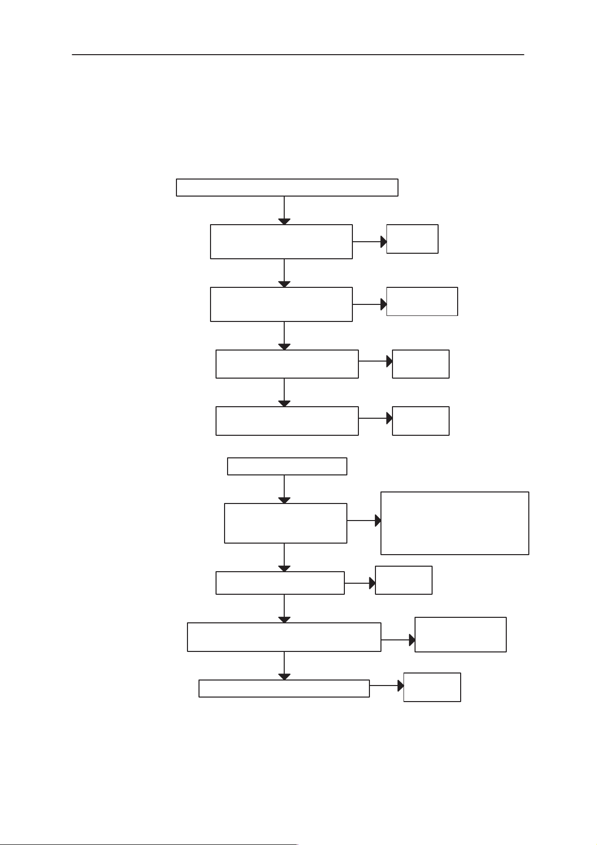
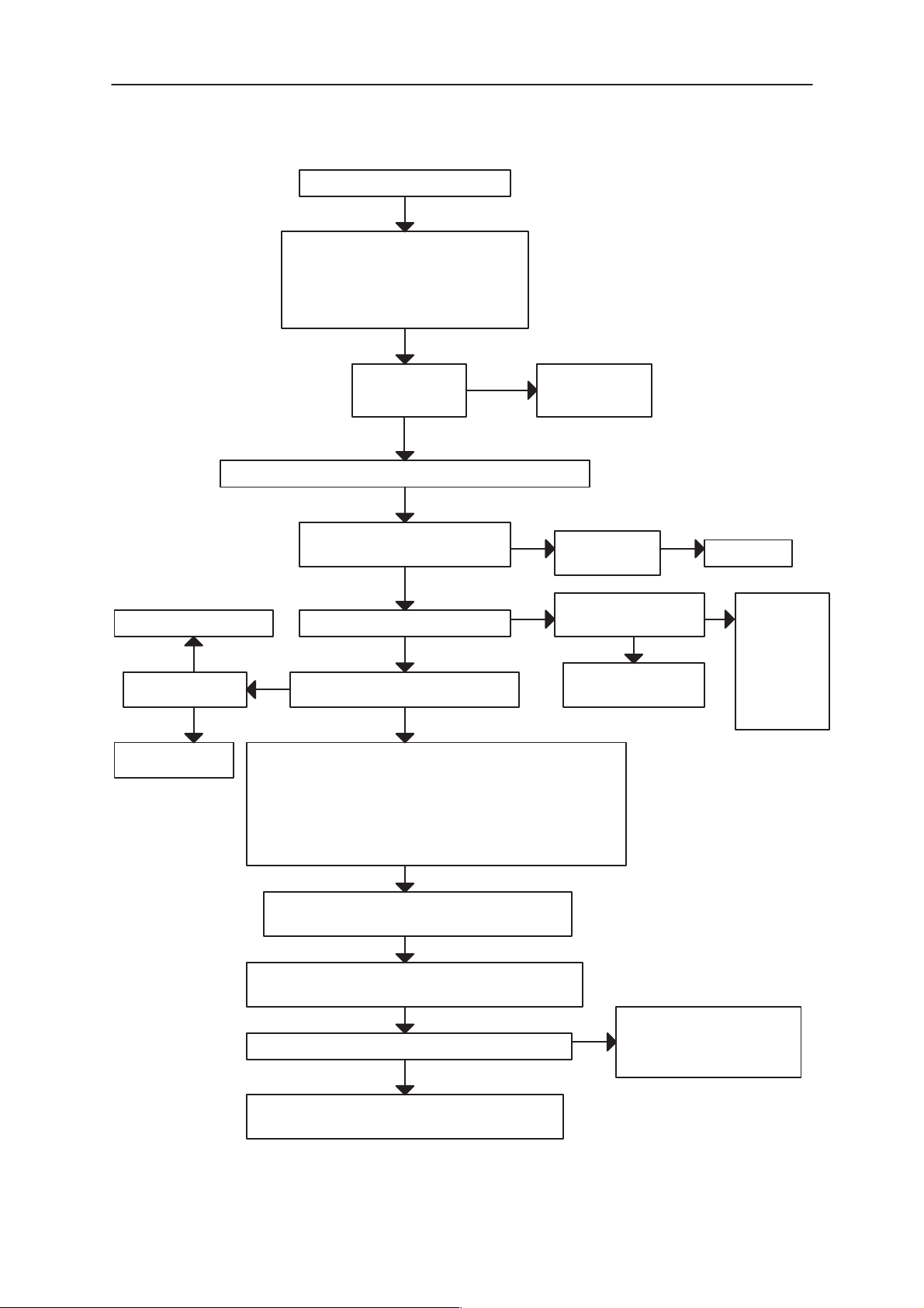
CMT is totally dead
Phone is totally dead
YES
J111
VBAT is 3.6 V
YES
J113 (PWRONx) 3.6 V
NO
Failure in VBAT line
Check X160,L103
Check shortcircuits
NO
Technical Documentation
This means that CMT doesn’t take current at all when
the power switch is pressed or when the Watchdog
Disable signal (J113) is rounded. Used battery voltage must be at least the nominal, 3.6 V.
Faulty circuit N110
YES
J109 (VBB) 2.8 V
N110 pin 25 (VXO) 2.8 V
when PWR switch is pressed
or watchdog disable pin is grounded
YES
See section: Power Doesn’t Stay On
Figure 1. Trouble Shooting Diagram for Phone is totally dead failure
PWRONX level (J113) low when
NO
PWR switch is pressed or
watchdog disable pin is (J100)
grounded
Faulty circuit N110
YES
Check V195, R195
NO
Check UI module
Page 7 – 8
Original 02/99
Page 9
PAMS
RAE–2
Technical Documentation
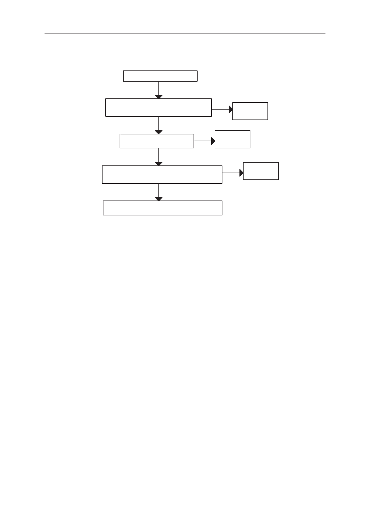
Power doesn’t stay on or phone is jammed
Normally the power will be switched off by CCONT (N110) after 30 seconds, if the watchdog of the CCONT can not be served by software. The
watchdog updating can be seen by oscilloscope at pin 50 (DataselX) of
CCONT. In normal case there is a short pulse from ”1” –> 0 every 8 seconds.
The power off function of CCONT can be prevented by connecting a short
circuit wire from CCONT pin 29 (or J113) to ground.
Power doesn’t stay on or phone is jammed
YES
CCONT watchdog is served?
(pin 50 pulses 1 –> 0)
NO
YES
Troubleshooting
software is able to run
check UI module
If power is switched off
after few seconds, check
BSI and BTEM lines
connect the shortcircuit wire from J113 to ground (watchdog)
OK
check C213, R213
YES
J706 (RFC) 13 MHz
800 mV min
NO
check buffer V702 and
VCXO G690
J109 (VBB) 2.8V
J704 (VXO) 2.8V
YES
J240 master reset (Purx) =”1” (2.8V)
YES
NO
J219: 13MHz sine wave
clock signal: 500 mVpp min.
YES
Open pins or faulty circuit:
D200, D210, D221, N110
NO
VBAT is correct
3.6 V
NO J241 sleep clock (SLCK)
square wave 32 kHz
Faulty circuit N110
or over loaded PURX line
YES
YES
N110 is faulty
N110 is faulty
YES
NO
32 kHz in J100?
check PDA 32kHz
circuit and its
connections to
Figure 2. Trouble Shooting Diagram for Power Doesn’t Stay On or phone is jammed failures
NO
CMT
Original 02/99
Page 7 – 9
Page 10
RAE–2
PAMS
Troubleshooting
Technical Documentation
Display Information: Contact Service
This fault means that software is able to run and thus the watchdog of
CCONT (N110) can be served. Selftest functions are run when power is
switched on and the software is started to execute from flash. If any of the
self–tests fails, Contact Service text will be shown on the display. Find
out which circuit is faulty using the WinTesla software (select from Testing
menu item Self Tests... and WinTesla shows which circuit are not passed
selftests).
The phone doesn’t register to the network or phone doesn’t make a call
If the phone does not register to the network or the phone does not make
a call, the reason could be either the baseband or the RF part. The phone
can be set to wanted mode by WinTesla service software and determinate
if the fault is in RF or in baseband part (RF interface measurements).
The control lines for RF part are supplied both the System Asic (MAD2;
D200) and the RFI (Cobba; N250). MAD2 handles the digital control lines
(like synthe, TxP etc.) and Cobba handles the analog control lines (like
AFC, TxC etc.).
The DSP software is constructed so that the operation states of DSP
(MAD2) can be seen in external flag (DSPXF) output pin (J222). After
power up, the DSP signals all completed functions by changing the state
of the XF pin.
1. DSP initialization done
2.Synchronization to network
done
3. Registrarition to network
done.
1 2 3
Page 7 – 10
MAD2 (DSPXF)
J222
Original 02/99
Page 11
PAMS
RAE–2
Technical Documentation
init
initialize
1
patch code
download
2
dsp
constants
download
initialization
done
Troubleshooting
MAD2 (DSPXF)
J222
channel
scan starts
PSW
search last PSW
OK
3
send RACH
RACH OK
go SDCCH
imediate assigment
OK
synchronization
OK
MAD2 (DSPXF)
J222
MAD2 (DSPXF)
J222
Original 02/99
Figure 3. The states of DSP after power on
Page 7 – 11
Page 12
RAE–2
PAMS
Troubleshooting
Phone doesn’t register to the network
or
phone doesn’t make a call
YES
Analog supply voltage VCOBBA is >2.7 V)
at testpad J110
YES
Analog reference voltage Vref is 1.5 V
at J107
YES
Supply voltage VCP (N110 pin 32) > 4.8 V
Supply voltage VRX (N110 pin 9) > 2.7 V
Supply voltage VSYN_1 (N1 10 pin 15) > 2.7 V
Supply voltage VSYN_2 (N1 10 pin 4) > 2.7 V
during the receiving slot
Supply voltage VTX (N110 pins 11, 20) > 2.7 V
during the transmitting slot
NO
Check VCOBBA line
and N110 (CCONT)
NO
Check
R251
NO
Technical Documentation
Fault in N110 (CCONT)
or D200 (MAD2)
YES
Synthesizer lines: SEna (N690 pin 7),
SClk (N690 pin 5)
SData (N690 pin 6)
pulses 0 –> 1 during receiving slot
YES
NO
Fault in
D200 (MAD2)
RF control lines: RxC (N690 pin 36) 0 –> 2.3 Vmax during receiving slot
AFC (R547) 0 – 1.2 V typ. during receiving slot
YES
Analog data signal RxIP (N690 pin 24) 0–> 1.5 V DC during receiving slot
Analog data signal RxIN (N690 pin 23) 0–> 1.5 V DC during receiving slot
Used benefit signal is biased to DC and its amplitude is 50 mVpp
nominal and frequency is 13 MHz
YES
NO
DAX signal (J254) pulses 1 –> 0 during receiving slot
YES
RF control lines: TxC (N690 pin 34) 0 –> 2.3 Vmax during transmit slot
TxP (N690 pin 32) 0–>1 (2.8 V) during transmit slot
YES
NO
Fault in
N250 (COBBA)
NO
Fault in
N250 if DC is failed
Check
RF part if benefit signal is failed
Fault in
N250 (COBBA)
Fault in
NO
N250 if TxC is failed
Check
D200 if TxP is failed
Page 7 – 12
Analog data signals: TxIN (N690 pin 3) 0–> 0.8 V DC during transmit slot
TxIP (N690 pin 4) 0 –>0.8 V DC during transmit slot
TxQN (N690 pin 1) 0 –>0.8 V DC during transmit slot
TxQP (N690 pin 2) 0 –>0.8 V DC during transmit slot
Used benefit signal is biased to DC and its amplitude is 300 mVpp
nominal and frequency is 64 kHz
Figure 4. The phone doesn’t register or doesn’t make a call
NO
N250 (COBBA)
YES
Check
RF part
Original 02/99
Fault in
Page 13
PAMS
RAE–2
Technical Documentation
SIM card is out of order
The hardware of the SIM interface from the MAD2 (D200) to the SIM connector (X150) can be tested without SIM card. When the power is
switched on and if the BSI line (X160;2) is grounded by resistor, all the
used lines (VSIM, RST, CLK, DATA) rise up to 5 V four times. Thus ”In-
sert SIM card” faults can be found without SIM card. The fault information ”Card rejected” means that the ATR message (the first message is
always sent from card to phone) is sent from card to phone but the message is somehow corrupted, data signal levels are wrong etc. or factory
set values (stored to the EEPROM) are not correct.
Card Rejected fault
YES
VSIM is according the specification
VSIM = 2.8 V min (with 3 V SIM card)
VSIM = 4.5 V min (with 5 V SIM card)
NO
N110 (CCONT)
Troubleshooting
faulty circuit
YES
The ATR data can be seen at pin 43
(CCONT, N110)
YES
The ATR data can be seen
at pin 44 (CCONT, N110)
YES
SIMIOControl line (N110 pin 39)
is ”1”during the ATR message
YES
Check D200
NO
Fault in
NO
N110 (CCONT)
NO
Fault in
D200 (MAD2)
Check X302, R124,
X150 and shorcircuit
in V140, R141
Insert SIM card fault
YES
Voltage level < 1.5 V
at pin 2 of D100 when
BSI resistor is connected
YES
VSIM, DATA, RESET and CLOCK lines
rises up to 5 V after power on at pins
of SIM card
NO
VSIM(36), DATAO(43),SIMRSTO(42) and SIMCLKO(38) lines
rises up to 5 V after power on at pins of N110 (CCONT)
NO
SIMPWR(30), DATAA(44), SIMRSTA(40), SIMCLK(41) and
SIMIOC(39) lines rises up to 2.8V after power on pins of N110
NO
NO
Check
R120, R122, X160
YES
Check
SIM card and SIM
reader connectors
YES
Check X105,
R124, R125,
R128, V140,
R141
YES
faulty circuit
N110 (CCONT)
Original 02/99
Check again that voltage level at pin 2 (SIMCardDetX) of D110 is lower than 1.5V
If it is, change D200
Figure 5. Troubleshooting for SIM card faults
Page 7 – 13
Page 14
RAE–2
PAMS
Troubleshooting
Audio fault
Troubleshooting tree for Audio fault:
Uplink (microphone) and downlink (earphone) are broken
Voltage at resistor R260 is 2.8 V
(without external audio devices)
HOOKDET
Voltage at resistor R261 is 2.8 V
(without external audio devices)
HEADDET
Frequency at J256 is 1 MHz, square
wave 2.8 Vpp
YES
YES
YES
Technical Documentation
NO
Check
R259, R260
NO
NO
Check
R257, R256, R261
Fault in
N250 (Cobba)
YES
Frequency at J257 is 8 kHz, square
wave 2.8 Vpp
Uplink (microphone) is broken
YES
Voltage at pin 1 of V271 is 1.8 V
Voltage at pin 3 of V271 is 0.3 V
during a call
YES
DC voltage at capacitors C273 and
C274 is 1.4 V during a call
YES
Analog audio signal (few millivolts) at capacitors C273
and C274 during a call
YES
Digital PCM data at J255 during a call
NO
NO
NO Fault in
Fault in
N250 (Cobba)
Check microphone, mic connections to
PCB and micbias components V250...
If OK, check that micbias control line
is (V270 base) 2.8 V during a call.
If no there is fault in D200 (MAD)
N250 (Cobba)
NO
NO
Check
C273, C274 and PCB
routings
Fault in
N250 (Cobba)
Page 7 – 14
Figure 6. Trouble Shooting Diagram for Audio Failure
Original 02/99
Page 15
PAMS
RAE–2
Technical Documentation
Digital PCM data at J258 during a call
DC voltage at capacitors C252
and C256 is 1.4 V during a call
Analog audio signal (some ten millivolts) at C252 and
C256 during a call
Check earpeace connections to PDA module and
earpiece signal routing from CMT to PDA.
Downlink (earphone) is broken
YES
YES
YES
YES
NO
NO
N250 (Cobba)
Fault in
D200 (MAD2)
Fault in
NO
Troubleshooting
Fault in
N250 (Cobba)
Figure 7. Trouble Shooting Diagram for Audio Failure
Original 02/99
Page 7 – 15
Page 16
RAE–2
PAMS
Troubleshooting
Charging fault
When you are charging totally empty battery, remember that start–up
charging might take 2 minutes with ACP–9 charger and several minutes
with ACP–7 charger. During this time display is blank.
If charger is not
NMP approved type
then the software
doesn’t start charging.
Remove and reconnect battery and
charger few times
before you start to
measure module.
This check ensure if
module fault really
exist.
Display Information: Not charging
YES
Technical Documentation
Nothing happens when charger is connected
YES
Voltage level at pin 60 of CCONT (N110)
is higher than 0.4 V when charger is connected
YES
Check with WinTesla software if SW has
detected charger and measured charger
current and voltage properly.
YES
Perform Energy Management
Calibration with WinTesla software and JBE–1 set and recheck
charger detection. If still fails
(CHAPS or CCONT) is broken.
NO
NO
Check
X170, F170
L170 and R170
Fault in N110
(CCONT)
Voltage level at pin 62 of CCONT (N110)
is about 0.45 V when power is connected.
BSI resistor value should be 33 k
YES
Voltage level at pin 63 of CCONT (N110)
is about 0.5 V when power is connected
BTEMP resistor value should be 47 k
YES
Check with WinTesla software if SW is
detected approved charger and measured
charger current and voltage properly.
YES
32 Hz square wave frequency at pin 7 of CHAPS (N120)
YES
Voltage levels at pins 5 and 12 of CHAPS (N120)
are same as VB
YES
Voltage levels at pins 5 and 12 of CHAPS (N120)
rises when charger is connected
NO
NO Check
NO
Check
X160, R121, R122,
D100, R123 and
VSYS = 2.8V
X160, R121, R122
Perform Energy Management
Calibration with WinTesla software and JBE–1 set and recheck charger detection, charger voltage and current. OK?
YES
NO
NO
NO
Charging?
Check
R131, N120
(CHAPS)
Fault in
N120 (CHAPS)
NO
Fault in N110
(CCONT) or
SW corrupted
Fault in
N110 (CCONT)
Page 7 – 16
Figure 8. Trouble Shooting Diagram for Charging Failure
Original 02/99
Page 17

PAMS
RAE–2
Technical Documentation
Flash programming doesn’t work
The flash programming is done over the system connector X170.
In flash programming error cases the flash prommer can give some in-
formation about a fault. The fault information messages could be:
– MCU doesn’t boot
– Serial clock line failure
– Serial data line failure
– External RAM fault
– Algorithm file or alias ID don’t find
– MCU flash Vpp error
In cases that the flash programming doesn’t succeed there is a possibility
to check short circuits between the memories and the MCU (MAD2).This
test is useful to do, when the fault information is:
MCU doesn’t boot,
Serial clock line failure or
Serial data line failure.
Troubleshooting
The test procedure is following:
1. Connect the short circuit wire between the test points J229 and ground.
2. Switch power on
3. If the voltage level in testpoint J203 is 2.8 V (”1”), the interface is OK. If
there is a short circuit, the voltage level in testpoint J203 stays low and
32kHz square wave signal can be seen in the lines which are already tested.
One must be noticed that this test can be found only short circuits, not
open pins. Also upper data lines (15:8) of flash circuit D210 are not included to this test.
Original 02/99
Page 7 – 17
Page 18
RAE–2
PAMS
Troubleshooting
passed
Technical Documentation
CCONT pin 54
J240
MAD pin N3
SRAM pin 20
MAD pin B15
J203
(PURX)
(MCUAD0)
(FlashRP)selftest
Figure 9. MAD selftest indication after power on (passed)
Page 7 – 18
Original 02/99
Page 19
PAMS
RAE–2
Technical Documentation
Flash programming doesn’t work
If the fault information from the prommer is:
Note:
When
Relink
OK,
PDA display
shows text
”Relink enabled”.
connect the short circuit wire J113 (WDOG) to ground
EEPROM (D240) pin 8 (VBB) 2.8 V
YES
a) MCU doesn’t boot
b) serial data line failure
c) serial clock line failure
Check ReLink
OK
OK
J704 (VXO) 2.8 V
YES
NOT OK
NO
PDA fault
VBAT is correct
3.6 V
Troubleshooting
YES
N110 is faulty
check C213, R213, V702 ...
YES
J706 (RFC) 13 MHz
800 mV min
NO
check
VCXO G690
NO J100 sleep clock (clk32k)
J240 master reset (PURX) = ’1’ (2.8 V)
YES
NO
check also pullup and pulldown resistors: R216, R215, R201
Enable the selftest function of D200 by connecting
shortcircuit between testpoints J229 and ground
Connect an oscilloscope to testpoint J203 and switch
Voltage level rises to ”1” after power on at testpoint J203
J219: 13 MHz sine wave
clock signal: 500 mVpp min.
YES
Check that following lines are correct:
FCLK (MBUS) line: X170 pin 7 –> J208
FTX (fbus_tx) line: X190 pin 38 –> J207
FRX (fbus_rx) line: X190 pin 37 –> J206
and series resistors R240
GND : X170 pin 1 –> GND
OK
power on
YES
or overloaded PurX line
square wave 32 kHz
YES
Faulty circuit N110
NO
There is a shortcircuit
somewhere in memory control
lines or MCU address lines or
MCU lower (7:0) data lines
NO
pin 14 –> J100
Check 32kHz
clock line
X173 pin 9
or
C190 pin 14
There could be open pins in circuits D200 (D210, D230)
If not, the PCB or D200 (D210, D230) is faulty
Figure 10. Trouble Shooting Diagram for flash programming doesn’t work (via system connector X170)
Original 02/99
Page 7 – 19
Page 20
RAE–2
PAMS
Troubleshooting
Flash programming doesn’t work
YES
If the fault information from the prommer is:
External RAM fault
YES
Check pins of SRAM (D220)
Check control lines of SRAM:
RAMSelX ...
Flash programming doesn’t work
YES
Technical Documentation
If the fault information from the prommer is:
Algorithm file or alias ID don’t find, ID is unknown etc.
Faulty component D210 or faulty lines
Flash programming doesn’t work
YES
If the fault information from the prommer is:
MCU flash Vpp error
YES
Vpp > 4.5 V in C212
YES
Check components C212, R211
OK
NO
YES
Vpp > 4.5 V in C131
NO
Check C131, C132, V116, N110...
YES
Check regulator N201
Faulty component D210
Figure 11. Trouble shooting Diagram for Flash programming doesn’t work (via system connector X170)
Page 7 – 20
Original 02/99
Page 21

PAMS
RAE–2
Technical Documentation
RF Fault
Here is a block diagram for repairing the RF section. First select the fault
and follow the diagram.
Required Servicing Equipment:
– PC for the Wintesla
– Power supply
– Digital multimeter
– Oscilloscope
– Spectrum analyzer
– GSM MS test set
– Signal generator
– RF probe
– Phone test jig
Test Points on BS8 Module
Troubleshooting
Test points are placed on baseband for service and production trouble
shooting purposes in some supply voltage and signal lines.
Because some of baseband signal are routed totally inner layers (due to
uBGA packages) some testpoints are added for these signals.
Original 02/99
Page 7 – 21
Page 22

RAE–2
PAMS
Troubleshooting
MCUGenIO15
McuGenIO1
DSPXF
RFClk
D220
MCUGenIO12
MCUGenIO13
MCUGenIO14
MCUGenIO11
MCUGenIO10
MCUGenIO09
MCUGenIO8
D210
ExtSysRSTX
MCUAD19
Technical Documentation
Flash Chip Select
MCUAD18
Flash Write Protection
N120
AccTXData
D200
AccRxData
McuGenIO4
PCMRxData
TestMode
PCMTxData
PCMDCLK
PCMSLCK
COBBADAX
COBBACKL
RFIWrX
COBBAAd0
RFIRdX
ROW5LCDCD
COBBADa0
ResetX
MBUS
DSPGenOut1
VCORE
CCONTINT
PURX
GENSCLK
VBB
SLCLK
32kHz
V5V
GENSIO
N110
VCXOPwr
D250
VREF
The figure above describes and the next table lists the test points.
VB
PWRONx
VCOBBA
Page 7 – 22
Original 02/99
Page 23

PAMS
RAE–2
Technical Documentation
Test Point Name Description
J100 32kHz 32kHz clock from BS1 module
J103 CCONTINT CCONT interrupt output
J105 GENSCLK Serial data clock
J106 GENSIO Serial data
J107 VREF Reference voltage
J108 V5V Supply voltage for flash programming (Vpp) and RF circuits.
J109 VBB Supply voltage for digital circuits
J110 VCOBBA Supply voltage for analog circuits
J111 VB Battery voltage
J112 VCORE Supply voltage for MAD c07 core
J113 PWRONx CCONT’s PWRONx / Watchdog disable signal
J203 ExtSysRSTX Testpoint for fault diagnostic. If missing, check power supply , PurX line and 13 MHz clock
signal.
J204 VCXOPwr Control line for VCXO module. If low, 13 MHz clock signal for baseband is disable.
J206 AccRxData FBUS RX
J207 AccTxData FBUS TX
J208 MBUS Serial data bus max 9600b/s. Flash programming clock
J209 McuGenio4 General purpose out in MAD
J211–J218 MCUGenIO(8:15) Test point for fault diagnostic. MCUDA(15:8)
J219 RFClk 13 Mhz System clock
J220 TestMode MAD test mode select input
J221 DSPGenOut1 General purpose DSP out
J222 DSPXF Test point for fault diagnostic.
J223–J224 MCUAD(18:19) Memory address signals
J225 Flash Chip Sel Flash chip select pin
J226 Flash Write Prot Flash write protection pin
J229 ROW5LCDCD Selftest pin. If shortcircuit is made between testpoint J229 and J230, the selftest will be
executed.
J232 COBBAAd0
J233 COBBADa0
J240 PurX Reset line from CCONT to MAD. If low, the BB circuits are in reset state.
J241 SLCLK 32 kHz clock from CCONT to MAD
J243 McuGenio1 General purpose input in MAD
J250 RFIRdX COBBA paraller interface read strobe
J251 RFIWrX COBBA paraller interface write strobe
J252 ResetX COBBA master reset
J253 COBBACLK COBBA 13Mhz clock
J254 COBBADAX COBBA paraller interface data available strobe
J255 PCMTxData COBBA PCM bus transmit data
J256 PCMDCLK COBBA bus data transfer clock
J257 PCMSCLK COBBA bus 8kHz frame sync
J258 PCMRxData COBBA PCM bus receive data
Troubleshooting
Original 02/99
Page 7 – 23
Page 24

RAE–2
PAMS
Troubleshooting
Transmitter fault
Troubleshooting tree for Transmitter fault:
Technical Documentation
Ref1
ref4
ref5
ref2
ref3
Page 7 – 24
Figure 12. Transmitter fault TX level 5
Original 02/99
Page 25

PAMS
RAE–2
Technical Documentation
Troubleshooting
ref6
ref7
ref8
ref9
ref10
ref11
ref12
Figure 13. Transmitter 1 TX level 5
Original 02/99
Page 7 – 25
Page 26

RAE–2
PAMS
Troubleshooting
Receiver fault
Troubleshooting tree for Receiver fault:
Technical Documentation
Page 7 – 26
Original 02/99
Page 27

PAMS
RAE–2
Technical Documentation
AFC Fault
Troubleshooting tree for AFC fault:
Troubleshooting
Original 02/99
Figure 14. AFC
Page 7 – 27
Page 28

RAE–2
PAMS
Troubleshooting
1st IF
Troubleshooting tree for First IF fault:
ref19
ref21
Technical Documentation
ref20
N690
ref22
ref23
ref24
Page 7 – 28
Figure 15. 1st IF 71MHz
Original 02/99
Page 29

PAMS
RAE–2
Technical Documentation
2nd IF
Troubleshooting tree for Second IF fault:
ref25
ref26
Troubleshooting
ref27
ref28
ref31
ref29
ref30
900X910
Original 02/99
Figure 16. 2nd IF 13MHz
Page 7 – 29
Page 30

RAE–2
PAMS
Troubleshooting
UHF LO
Troubleshooting tree for UHF LO fault:
Technical Documentation
Page 7 – 30
Figure 17. UHF LO
Original 02/99
Page 31

PAMS
RAE–2
Technical Documentation
VHF LO
Troubleshooting tree for VHF LO fault:
Troubleshooting
2.5V
1.2V
Figure 18. VHF LO
1.8V
Original 02/99
Page 7 – 31
Page 32

RAE–2
PAMS
Troubleshooting
PDA Troubleshooting and Service
The purpose of this sectionis to provide methods to find the component
that is malfunctioning in the PDA module of the RAE–2. Due to the large
integration scale of used components, it is always not possible to point
the faulty component for sure. However the flow diagram introduced here
is made to fulfill the aim as well as it is possible.
Required Servicing Equipment:
– PC for the Wintesla
– Service battery BBS–5
– Service cable DAU–9C
– Combox TDC–4
– IR transceiver module JLP–1
– digital multimeter
– oscilloscope
– frequency counter (optional)
Technical Documentation
Block Diagram
The block diagram of the BS1 PDA is described in the next figure:
Page 7 – 32
Original 02/99
Page 33

PAMS
RAE–2
Technical Documentation
PDALCD
GND
LCD PWR IF(6:0)
PWRU
V28_3
VPDA
D6:0
SA1:0
Charging
io(3:0)
Backupbattery
control (6:0)
VBACK
X32kHz out
X32kHz in
sio(1:0)
VSYS
VBATT
FLASH
1Mx16
LCD(10:0)
MMC(3:0)
BS2
Flex connector
FLASH
1Mx16
MA(11:0)
D(15:0)
Am486 CPU
SA(21:0)
SD(15:0)
JTAG(4:0)
io(5:0)
Softkeys
FLASH
1Mx16
FBUS_RXD
FBUS_TXD
MBUS
C(3:0), R(1:0)
C(7:0), R(9:0)
io(1:0)
RS_IF(2:0)
io(3:0)
x32
CMT
Keypad
Troubleshooting
CMT LCD
CMTLCD(5:0)
X800
BS1
QWERTY
Keyboard
Audio
Earpiece
HF
HF_IF(1:0), EAR(1:0)
VBATT
IR transceiver
GND
FBUS_RXD
DRAM
1Mx16
Test–
pads
FBUS_TXD
FBUS_TXD2
MBUS
BoBo
Connector
Memory Card
Figure 19. BS 1 PDA block in RAE–2 product
CMT
PWRKEY
C4:0,R3:0
System connector X810
GND
X830
BS8
Original 02/99
Page 7 – 33
Page 34

RAE–2
PAMS
Troubleshooting
BS1 PDA Components
The following components of the BS1 have an dramatic effect to the
functionality of the module, a fault in any of these may cause the module
to appear totally ‘dead’:
– PDA power unit
– CPU
– PLL clock generation circuit
– UCS Flash chip
If the device has some functionality, then the following components, along
with the ones above, can be tested:
– DRAM chip
– CS1 and CS0 Flash chips
– Handsfree speaker circuitry
Technical Documentation
– Earpice circuitry
– IR transceiver
– keyboard
– LCD module
– Memory Card interface
– Serial connections (FBUS and system bus)
Page 7 – 34
Original 02/99
Page 35

PAMS
RAE–2
Technical Documentation
BS1 Troubleshooting
The highest level of the RAE–2 PDA troubleshooting diagram is shown in
the following figure. All the diagrams are made assuming that there is no
visible faults, such as short–circuits or loose pins, on the PDA.
The module check begins with connecting the supply voltage to the PDA.
If the current consumption differs a great deal from the normal limits, it is
good to proceed to the Power–On check.
During BIOS detects some error during POST it tries to beep the buzzer
for further fault analysis for the user. The POST beep codes, number of
beeps are in the Appendix A on p.54.
If the current consumption is OK, it can be tried if the wintesla service
software is able to get connection to the PDA. If the target PDA does not
respond to the pings from the host, it is good to check the Power–On procedure.
Troubleshooting
When the PDA responds to the wintesla, further peripheral tests may be
carried out. The execution order is not significant and it may be freely
changed. Along with the actual tests, wintesla offers advanced methods
for isolating the possible cause of the fault.
After all the functional tests are working, the device under test should be
re–booted, and the normal usability of the GEOS, along with the CMT
module should be checked before the PDA can be considered to be fully
functional.
Original 02/99
Page 7 – 35
Page 36

RAE–2
PAMS
Troubleshooting
PDA MODULE CHECK
Connect VBatt
Current
consumption
OK?
YES
Respond
to wintesla?
YES
POST–code
check
PLL clock circuits
check
NO
NO
Technical Documentation
See Power On
malfunctions
See Power On
malfunctions
DRAM
check
Flash memories
check
LCD
check
Backlight
check
keyboard
check
Serial connections
check
IR
check
Lid Switch
check
Handsfree speaker
check
Earphone
check
Page 7 – 36
Memory card interface
check
OS BOOT
GEOS
Usage Test
OK
Figure 20. The highest level of the PDA troubleshooting diagrams
Original 02/99
Page 37

PAMS
RAE–2
Technical Documentation
Power–on malfunction
The following picture illustrates the troubleshooting diagram for Power–
On malfunctions.
Start
POST
BEEP Code
error?
YES
NO
Vsys
OK? E312
YES
Troubleshooting
NO
CPU
related error?
YES
Memory
fault
in Flash
NO
Program
V alid boot code
Check
External RS
Memory
flash
NO
YES
fault
NO
INT_PLL
OK? J400
(1.4MHZ)
YES
Bus activity?
D/A, R/W, CS
J440–J449
YES
Reboot and ping
from the wintesla
while in TestMode
Respond to
Power On
OK!
5.
PING from host?
YES
NO
NO
Check
PLL–circuit
Reset OK ?
J449
Check PDA
power unit
Original 02/99
Figure 21. Troubleshooting of the power–on malfunction
Page 7 – 37
Page 38

RAE–2
PAMS
Troubleshooting
Power Circuitry Check
The following figure illustrates how to check power circuits. The upper
part of the flowchart must be passed before the swicthable voltages (lower part of the flowchart) can be considered to be alright.
The LCD temperature compensation affects the LCD bias voltage values.
Because of this temperature compensation, the LCD bias voltages are
different in different temperatures, but anyway bias voltage maximum and
minimum values should differ 4 Volts from the typical value (DAC 63) in
every temperature.
Figure on the next page.
Technical Documentation
Page 7 – 38
Original 02/99
Page 39

PAMS
RAE–2
Technical Documentation
Power
check
NO
NO
NO
Check
Input filter
Power ASIC
fault
VBATT
OK?
YES
VPDA
OK?
YES
VBACK
OK?
Check
CMT
YES
Board to board
connector
OK?
NO
Troubleshooting
Change
connector
YES
VSYS
OK?
YES
RESET
OK?
YES
(If you can not enable some voltage, try enable some other to be sure that CPU and bus from/to it is OK)
Select
I/O functions/
Phaser calibration
in WinTesla
LCDTEMP
OK?
NO
Hinge flex
OK?
YES
NO
NO
NO
DAC value 63
BATTDET
OK?
SELECT TROUBLE RELATED BRANCH
Select
I/O functions/
Phaser calibration
in WinTesla
Select max.
V17OUT
V17OUT
MAX voltage?
YES
Select
YES
NO
Power ASIC
fault
Power ASIC
fault
YES
VCOMP1
OK?
Select
I/O functions/
Signal control
in WinTesla
Enable LCD
V28_1
OK?
NO
Signal control Signal control
PDA LCD
locig
voltage OK
Check
R461 – R463
R469
R493 – R495
YES
N496
OK?
Select
I/O functions/
in WinTesla
Enable IR
V28_2
OK?
NO
NO
I/O functions/
YES
IR–
transceiver
logic
voltage OK
Change
N496
Select
in WinTesla
Enable
MMC power
V28_3
OK?
NO
YES
Memory
card
power OK
NTC OK
on UI?
YES
Power ASIC
fault
Original 02/99
V17OUT
typical vol–
tage?
YES
PDA LCD
bias voltage OK
Figure 22. Power unit troubleshooting diagram
NO
Power ASIC
fault
Page 7 – 39
Page 40

RAE–2
PAMS
Troubleshooting
Technical Documentation
Troubleshooting Diagram of the PLL clock generation circuit
The following diagram illustrates how to check PLL clock generation circuits.
PLL Circuit
check
X32_CLK
OK?
J401
YES
NO
Vback OK?
E307
YES
NO
Check power
ASIC N450
PLL intermediate
voltage 1.2V?
J430
YES
check
XIP
flashes
XIPs
OK?
NO
YES
NO
1.4MHZ
OK?
J400
YES
PLLs
OK
components on
Discrete
PLL OK?
YES
CPU
fault
XTAL OK?
32kHz
J434, J435
NO
NO
Change faulty
discrete
component
Check
XTAL
Page 7 – 40
Figure 23. PLL clock generation circuit check
Original 02/99
Page 41

PAMS
RAE–2
Technical Documentation
Troubleshooting Diagram of the DRAM
The following figure illustrates how to check DRAM. Open DRAM test in
WInTesla and select RandomTest. If test passed DRAM should be alright.
If the test is not passed, run test again and measure the data and control
lines activity.
DRAM
check
Start the DRAM
Random test
Troubleshooting
DRAM test
succesful?
YES
DRAM
OK
NO
Figure 24. DRAM troubleshooting diagram
Bus activity?
(R/W, CAS, RAS, ADD)
J446–J449
J4555,J456
YES
DRAM or
CPU fault
NO
CPU
fault
Original 02/99
Page 7 – 41
Page 42

RAE–2
PAMS
Troubleshooting
Troubleshooting Diagram of the Flash memories
The PDA comprises two kind of flash memories, two XIP (eXecute In
Place) flashes and one RFD flash.
The XIP flash can be checked by comparing image checksum and calculated checksum.
If you can read and write from/to RFD flash, it is likely to be OK.
Technical Documentation
Page 7 – 42
Original 02/99
Page 43

PAMS
RAE–2
Technical Documentation
XIP
Flashes
check
Read
image checksum
Compare
calculated checksum
and
image checksum
Are
Checksums
equal?
YES
XIP flashes
OK
NO
Bus activity ?
(AD, D, CE, WE)
J441, J442
J453, J454
NO
CPU
fault
YES
Troubleshooting
Flash fault
NO
Flash
status output
STSx(J451 or J452)
OK?
YES
CPU fault
RFD
flash
check
Write to
RFD flash
Read from
RFD flash
write and read
OK?
YES
RFD flash
OK
Flash fault
NO
NO
Figure 25. Flash memories troubleshooting diagrams
Bus activity ?
(AD, D, CE, OE, WE, WP)
J440, J442–J444
J453, J454
NO
CPU
fault
YES
status output
STSx (J450)
YES
Flash
OK?
CPU fault
Original 02/99
Page 7 – 43
Page 44

RAE–2
PAMS
Troubleshooting
Troubleshooting Diagram of the LCD
The idea of the following diagram of the LCD Check is to make the difference whether the LCD BS2 module or the PDA BS1 is broken. The case
where the fault is in the BS2 module is beyond the scope of this document. The fix in that case is likely the change of the whole module.
0.
Start
1.
NO
LCD ON?
1.1
Disconnect UI
flex
Technical Documentation
YES
5.
Test–patterns
OK?
YES
LCD OK!
NO
1.2 1.2.1
V28_1
OK? N450/22
YES
V17
OK?
E300
YES
1.4 1.5
UI flex OK?
NO YES
NO V28_OUT
1.2.2
CPU fault
1.3
NO V17_OUT
NO
active?
N450/61
NO
NO
1.3.1
active?
N450/60
1.3.2 Check
PDA PWRU
CPU fault
LCD control
signals OK?
J805–J808
YES
1.5.2
Page 7 – 44
1.4.1 UI flex
fault
Figure 26. Troubleshooting of LCD signals
1.5.1 LCD
module fault
Original 02/99
Page 45

PAMS
RAE–2
Technical Documentation
Troubleshooting Diagram of the PDA LCD Backlight
This troubleshooting diagram describe troubleshooting procedure on the
PDA LCD backlight. If PDA is OK, look then backlight troubleshooting procedure from next chapter UI TROUBLESHOOTING.
PDA LCD
Backlight
check
Enable
backlight
Troubleshooting
Check
hinge flex
connector
NO
Backlight
OK?
YES
Backlihgt
OK
NO
Disconnect
hinge
flex
Figure 27. PDA LCD backlight troubleshooting
Backlight
enable signal
(X800/24)
OK?
NO
CPU fault
YES
VPDA
OK?
(X800/51)
YES
Check
backlight
connections
on UI module
Original 02/99
Page 7 – 45
Page 46

RAE–2
PAMS
Troubleshooting
Troubleshooting Diagram of the PDA Keyboard
This section describe PDA keyboard troubleshooting procedure. Possible
cause to keyboard faults are keyboard interface in CPU, broken keymat
or keydomes (UI) . Also, dirty keymat or keypad area can cause the fault.
Keyboard
check
Start the
keyboard test
Technical Documentation
Press a QWERTY/
softkey
Keypress
regognized?
YES
NO
pressed
keyboard
All
keys
YES
OK
NO
Figure 28. Keypad troubleshooting diagram
Other
same row or
column keys
regognized?
NO
CPU fault
YES
pressed key
YES
hinge flex and
softkey domes on UI
Was
a lidkey
Check
NO
Keypad
or keymat
fault
Page 7 – 46
Original 02/99
Page 47

PAMS
RAE–2
Technical Documentation
Troubleshooting Diagram of the serial connections
External bus connection is alright if the device is PINGing, if not is good to
check system connector and discrete components on RX and TX lines.
External bus use RS232 data protocol, but signal voltage levels on PDA
and system connector are only 2.8V digital voltage levels. External buffer
cable needed (DLR–2) for connecting to PC.
Serial connection between CMT and PDA (FBUS) can be checked as following flow chart described.
FBUS
check
Troubleshooting
Open RS test
and run COM2
local loop test
COM2
local loop test
OK?
NO
CPU
fault
Remove CMT
YES
Figure 29. FBUS troubleshooting diagram
and connect
RX and TX
together on
board to board
connector
Run COM2
external loop
test
Check
CMT side
YES
COM2
external loop
OK?
NO
Check
board to board
connector
Original 02/99
Page 7 – 47
Page 48

RAE–2
PAMS
Troubleshooting
External
RS
check
PiNG
target?
NO
Test
connections
OK?
NO
Repair
test
connections
YES
YES
External
RS
OK
RX
signal OK?
(X810/8)
X810
V870, V871,
R806
OK?
YES
NO
YES
CPU
fault
Technical Documentation
TX
signal OK?
(X810/9)
NO
X810 and
V870
OK?
YES
Figure 30. External serial connection troubleshooting diagram
Page 7 – 48
Original 02/99
Page 49

PAMS
RAE–2
Technical Documentation
Troubleshooting Diagram of the IR connection
This section describe infrared connection troubleshooting procedure.
IR test need Combox TDC–4 with IR transceiver JLP–1.
Place PDA so that IR transceiver have clear light route to JLP–1 and run
the IR test. If test not passed follow flowchart to find out the fault.
IR shutdown is not in use.
Check
power ASIC
N450
YES
R301, C301
OK?
NO
V28_2
OK?
(N300/6)
YES
IR
check
IR
test
OK?
NO
test connections
Repair
test
connections
NO
External
Ok?
YES
Troubleshooting
Check
R300,
R302–R304
C300
NO
VPDA
OK?
(N300/1)
YES
IrDA
OK
YES
CPU fault
CPU fault
Figure 31. IR connections troubleshooting diagram
NO
COM1
local loop
test OK?
YES
IR–
transceiver
fault
NO
YES
NO
YES
TXD
OK?
(N300/3)
RXD
OK?
(N300/4)
Original 02/99
Page 7 – 49
Page 50

RAE–2
PAMS
Troubleshooting
Troubleshooting Diagram of the lid switch
The idea of this diagram is to find out whether the CPU or the reed relay
circuit is not working.
If CPU and reed relay circuit on PDA is alright, then possible cause of
fault is magnet in lid.
Lid
switch
check
Open
WinTesla
Signal control
Technical Documentation
Lid switch
OK
LID OPEN?
NO
LID_SWITCH_IF
high?
J310
NO
R310
OK?
NO
Change
R310
YES
YES
Place magnet
near the reed
relay
CPU
fault
Figure 32. Lid switch troubleshooting diagram
Select
Refresh
in WinTesla
YES
LID CLOSED?
NO
LID_SWITCH_IF
low?
J310
NO
Reed relay
fault
Page 7 – 50
Original 02/99
Page 51

PAMS
RAE–2
Technical Documentation
Troubleshooting Diagram of the HF Speaker
The idea of this diagram is to find out whether the CPU, loudspeaker, or
power amplifier or it circuitry is not working.
Start
VAMP OK?
R855/R856
YES
NO
Check
R891, R892 and
C880 – C882, C892
Troubleshooting
Signal from
COBBA OK?
J881
YES
PA–Enabled?
N880/1
NO
V880 NO
OK?
Check
CMT CPU
NO
YES
Check COBBA
on CMT
Signal amplified?
Change V880
Speaker fault
N880/5,8
YES
NO
HFPA–Fault
Original 02/99
Figure 33. HF–Speaker troubleshooting diagram
Page 7 – 51
Page 52

RAE–2
PAMS
Troubleshooting
Troubleshooting Diagram of the Earpiece
The following diagram illustrates how to check earpiece connections on
the PDA side.
Run the wintesla buzzer test. If the sound is not good then check earpiece connections as following flowchart illustrates.
Earpiece
connection
check
Start
buzzer
test
Technical Documentation
Buzzer
sound Ok?
NO
BZR_IF
signal OK?
J854
YES
VAMP OK?
(R855/R856)
NO
Check
R891, R892 and
C880 – C882,
C892
YES
NO
YES
Buzzer OK
Check PDA CPU
V872
and
V873
OK?
NO
Change faulty
component
YES
Check
Earphone
Page 7 – 52
Figure 34. Earphone troubleshooting diagram
Original 02/99
Page 53

PAMS
RAE–2
Technical Documentation
Troubleshooting
Troubleshooting Diagram of the Memory Card interface
To check the memory card interface:
Take a good memory card and place it in the memory card
connector.
Run Wintesla MMC test. If test failed then take memory
card out and run test again.
Measure memory card system voltage and bus signals
when test running.
If the signal and the card voltage are OK, then the interface is likely to be
OK. If everything is not alright check interface connections as the flowchart illustrate.
Memory Card
interface
check
Run
MMC
test
Test
OK?
NO
MMC_DAT,
MMC_CMD and
MMC_CLK
OK?
YES
MMC_SYS
OK?
NO
Enable
MMC power
in WinTesla
NO
YES
Board to
board and memory
card connectors
OK?
YES
CPU
fault
NO
Change
faulty
connector
V28_3
OK?
(X830/46)
YES
Check
CMT side
Original 02/99
NO
Check
Power ASIC
N450
Figure 35. Memory card interface troubleshooting diagram
Page 7 – 53
Page 54

RAE–2
PAMS
Troubleshooting
POST BEEP Codes
1 Memory refresh is not working.
3 Memory failure in 1st 64kB of memory.
4 Timer T1 not operational.
5 CPU test failed.
6 Gate A20 failure.
10 CMOS shutdown register failed.
13 Exhaustive low memory test failed.
14 Exhaustive extended memory test failed.
15 CMOS restart byte can’t hold data.
16 Address line test failed.
18 Interrupt controller failure.
Technical Documentation
Page 7 – 54
Original 02/99
Page 55

PAMS
RAE–2
Technical Documentation
UI Troubleshooting
Mechanical Troubleshooting
In mechanical failures it is better to replace a whole unit or module than try
to fix it in service. The replaceable units or modules on BS2 UI module are:
– BC2 CMT LCD module
– PDA LCD display
– UI PCB
– EL backlight panels
– Keydome sheets
Keyboard Troubleshooting
Troubleshooting
– Equipment: Resistance meter (multimeter)
– If CMT keyboard does not function when the lid is closed, it is possible
that reed relay (in the BS1 module) is damaged. If text ”Please close
cover” comes to CMT LCD when a CMT key is pressed when lid is
closed, the reed relay is probably damaged.
– Check that the dome sheets are properly placed. Improperly placed
dome sheet may cause malfunction of some key(s) or power down of
the CMT when a key is pressed.
Table 1. CMT keyboard checklist.
Non–functioning CMT keys Check components
6, 9, # R704, C707
1, 2, 3, Soft_left R705, C706
4, 5, Send, Up R705, C714
7, 8, End, Down R705, C713
0, *, Mode, Soft_right R706, C712
3, 6, Send, End, Mode R706, C708
9, Soft_left, Soft_right, Up, Down R707, C709
1, 4, 7, #, * R707, C710
2, 5, 8, 0 R708, C711
Original 02/99
Page 7 – 55
Page 56

RAE–2
PAMS
Troubleshooting
CMT LCD Module Troubleshooting
Start
No
Is display properly
on its place?
Remove and put the display back to its place and
test again.
Display shows unexpected
characters
LCD glass is probably
mechanically damaged. Inspect and re-
Yes
place.
What is the
problem?
Pixel line(s) missing.
Display does not work
Yes No
Is display properly
Yes
on its place?
Can Vout voltage be
measured from
J715 when display
is on its place.It
must be 6...9 volts.
Technical Documentation
No
Remove and put the display back to its place and
test again.
Yes
Problem might be some
randomize behavior or
unclean contact pads of
CMT LCD. Clean contacts and try again.
Problem might be elastomer or misaligned hinge
flex. Remove and connect hinge flex again.
Check elastomer.
Press some phone
key. Are GENSCLK
(J706), GENSDIO
(J707) OK and is
LCDRSTx (J708)
’high’?
No
Does display work OK?
Check C705 and in
BS2_10 R709.
Is VBB (J713) OK?
Yes
Remove LCD and check
the elastomer. Clean
contact pads on PCB and
try again.
No
No
– Testing equipment: Multimeter and oscilloscope.
Page 7 – 56
Yes
End
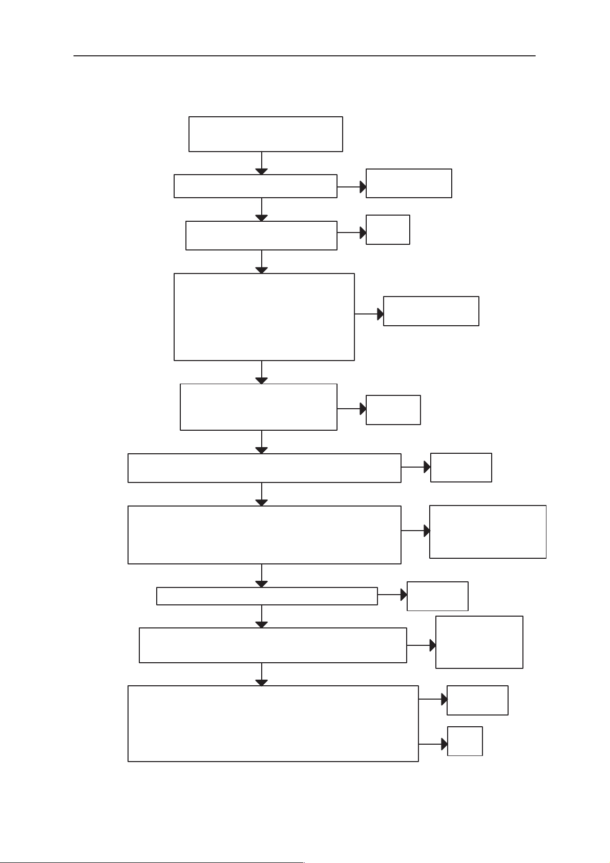
Figure 36. Flow chart for the troubleshooting of CMT LCD module.
Original 02/99
Page 57

PAMS
RAE–2
Technical Documentation
Troubleshooting
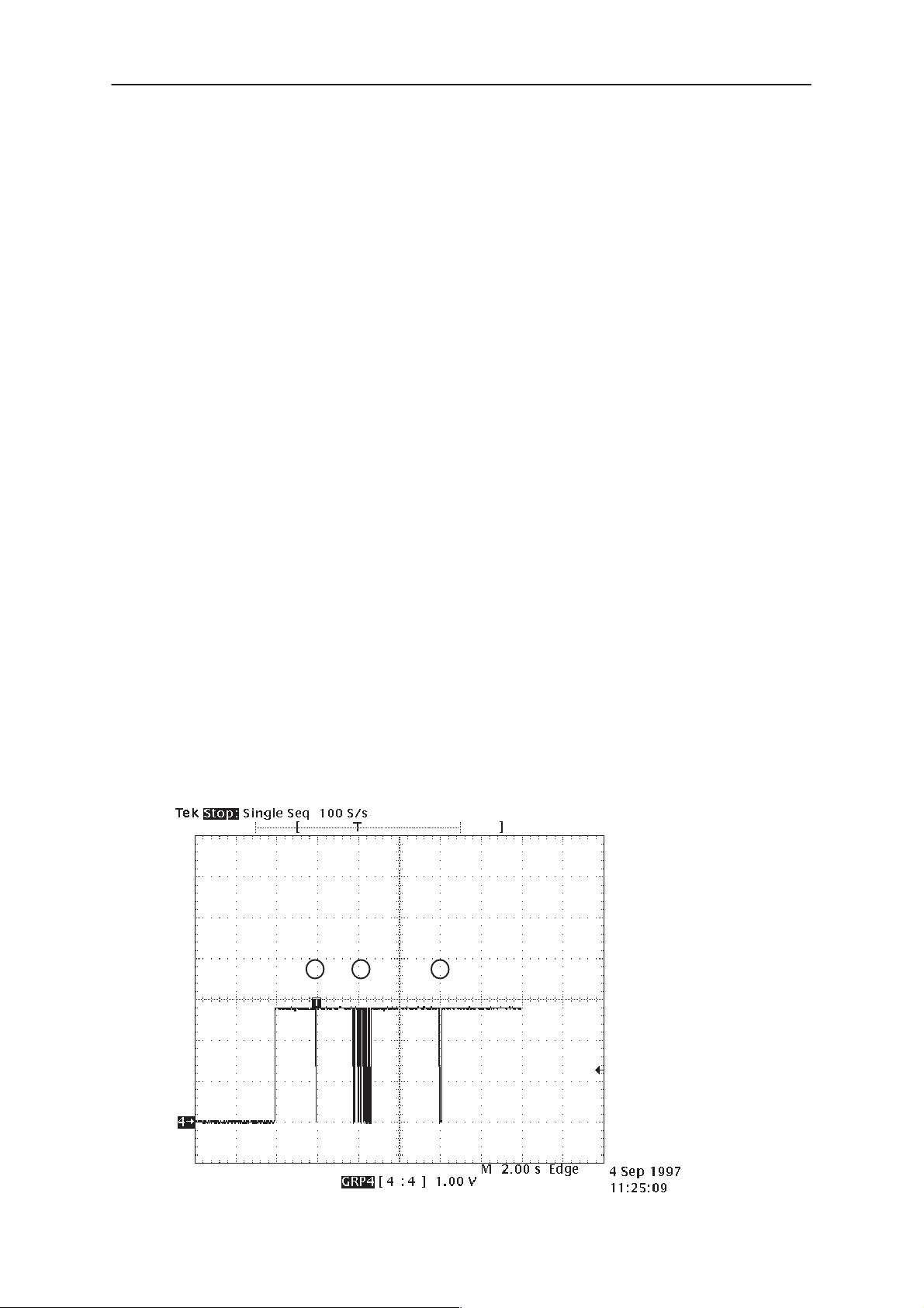
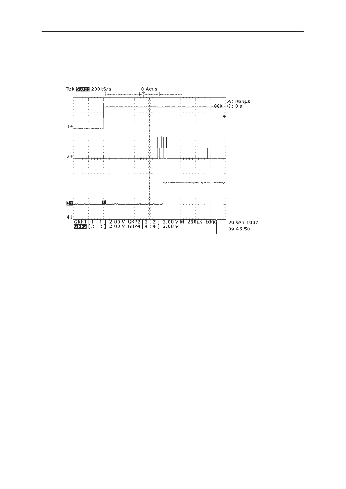
Figure 37. GENSCLK (J706) and LCDCSx (pin 5/H700) , LCD active after
pressing a key.
Original 02/99
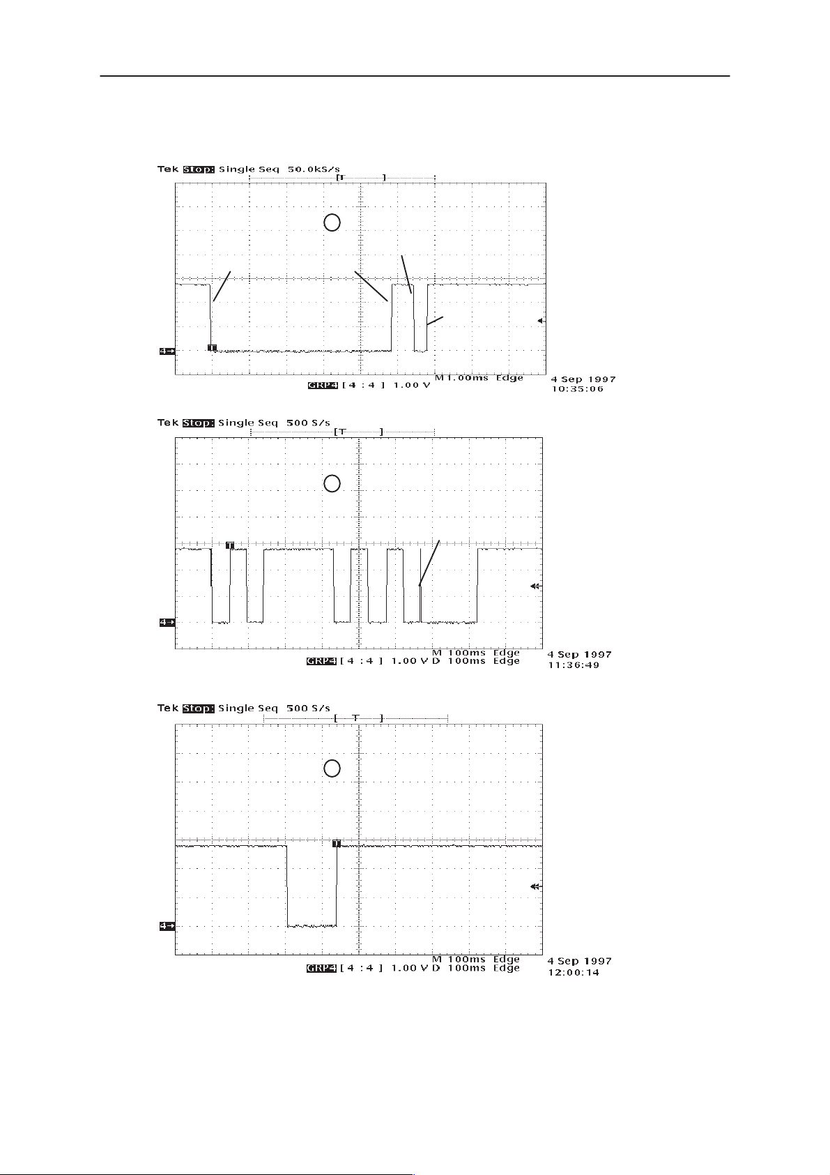
Figure 38. GENSCLK (J706) and LCDCSx (pin 5/H700), LCD inactive, serial
bus used for communication between MAD and CCONT.
Page 7 – 57
Page 58

RAE–2
PAMS
Troubleshooting
Technical Documentation
Figure 39. GENSDIO (J707)
Page 7 – 58
Original 02/99
Page 59

PAMS
RAE–2
Technical Documentation
PDA LCD Display Troubleshooting
START
What is wrong?
Large part of the
Make sure that the
flex of the display is
Yes
properly connected
to X730. Does the
display work now?
Check C740–C744
and in BS2_10
Yes
R736–R739. Does
the display work
now?
Are V28_1
(J700) and
LCD_ON (J701)
about 2.8V?
No
No
No
Yes
display is black
or dark blue or
pixel line(s) is
missing
LCD is mechanically
damaged. Replace
the display.
No
Bad picture qualityDisplay does not work
Check C740–C744
and in BS2_10
R736–R739. Does
the display work
now?
Yes
Make sure that the
flex of the display is
properly connected
to X730. Does the
display work now?
YesNo
Troubleshooting
Is V17_OUT (J709)
as specified?
No
Yes
Are FRM (J702), M
(J703), LC (J704)
and SCK (J705) as
specified?
Yes
Display is probably
damaged. Replace
it with a new
display.
No
Reason may be
misaligned hinge
flex. Remove and
connect flex
again and test
display again.
Does the display
work OK now?
Yes
END
No
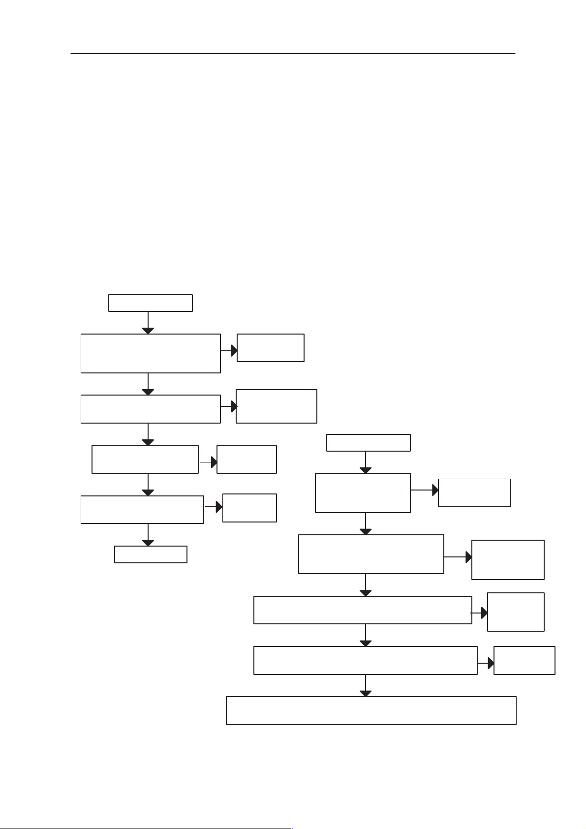
Figure 40. Flowchart for troubleshooting of the PDA LCD.
– Testing equipment: Multimeter and oscilloscope.
Original 02/99
Page 7 – 59
Page 60

RAE–2
PAMS
Troubleshooting
Technical Documentation
Figure 41. LCDD0 (J712)
Page 7 – 60
Figure 42. LC (J704)
Original 02/99
Page 61

PAMS
RAE–2
Technical Documentation
Troubleshooting
Figure 43. M (J703)
Original 02/99
Figure 44. SCK (J705)
Page 7 – 61
Page 62

RAE–2
PAMS
Troubleshooting
Technical Documentation
Figure 45. FRM (J702)
Page 7 – 62
Original 02/99
Page 63

PAMS
RAE–2
Technical Documentation
CMT Backlighting Circuit Troubleshooting
When troubleshooting the CMT backlighting circuit, remember that backlighting goes off after a certain period from the last key pressing.
START
Check that EL panel
Yes
contacts are OK.
Does the backlight
work now?
Is VPDA voltage OK
on UI board (J714)?
No
NoYes
Troubleshooting
Is the voltage of pin
1/N700 higher than
3.0 V?
Yes
Is driver circuit’s out–
put as specified
(6,7/N700)?
No
Are coil L700, diode V701,
capacitors C701–C703 and
resistors R700–R702
(R703 in BS2_10) OK?
Yes
Replace with new
circuit.
No
Yes
No Replace faulty com–
ponents. Does the
backlight work now?
Is CMT_BL_ON
signal voltage at
J710 about 2.8V?
Try with a new EL
panel. Does the
backlight work
now?
Yes
No YesInverter is damaged.
No
Yes
No
V702 or V703 is
damaged.
Replace them.
END
Reason may be
misaligned hinge
flex. Remove and
connect flex
again and test
display again.
Does the
backlight work
OK now?
Yes
No
Figure 46. Flowchart for troubleshooting of the CMT backlighting circuit.
Original 02/99
Page 7 – 63
Page 64

RAE–2
PAMS
Troubleshooting
PDA LCD Backlighting Circuit Troubleshooting
For PDA backlighting troubleshooting you can use test mode and WinTesla SW to set the backlighting on all the time.
START
Check that EL panel
Yes
contacts are OK.
Does the backlight
work now?
No
Technical Documentation
Is the voltage of pin
1/N730 higher than
3.0 V?
Yes
Is driver circuit’s out–
put as specified
(6,7/N730)?
No
Are coil L730, diode V730,
capacitors C736–C738 and
resistors R730–R732
(R733 in BS2_10) OK?
Yes
Replace with new
circuit.
No Replace faulty com–
No
Try with a new EL
Yes
panel. Does the
backlight work
now?
ponents. Does the
backlight work now?
No YesInverter is damaged.
Is VPDA voltage OK
on UI board (J714)?
Is PDA_BL_ON
signal voltage at
J711 about 2.8V?
Yes
Yes
No
NoYes
No
V731 or V732 is
damaged.
Replace them.
Reason may be
misaligned hinge
flex. Remove and
connect flex
again and test
display again.
Does the
backlight work
OK now?
Yes
No
Figure 47. Flowchart for troubleshooting of the PDA backlighting circuit.
– Testing equipment: Multimeter and oscilloscope. Note that voltage rating of the oscilloscope and probe must be over 250 V peak–to–peak.
Page 7 – 64
END
Original 02/99
Page 65

PAMS
RAE–2
Technical Documentation
Troubleshooting
Figure 48. Example of a typical EL driver output waveform,
measured between pins 6 and 7 of the driver.
Original 02/99
Page 7 – 65
Page 66

RAE–2
PAMS
Troubleshooting
Technical Documentation
Page 7 – 66
Original 02/99
 Loading...