

Page 1

PAMS Technical Documentation
NSM–2 Series Transceivers
System Module
Issue 1 12/1999 Nokia Mobile Phones Ltd.
Page 2

NSM–2
System Module
PAMS Technical Documentation
CONTENTS
Transceiver NSM–2 6. . . . . . . . . . . . . . . . . . . . . . . . . . . . . . . . . . . . .
Introduction 6. . . . . . . . . . . . . . . . . . . . . . . . . . . . . . . . . . . . . . . . . .
Operation Modes 6. . . . . . . . . . . . . . . . . . . . . . . . . . . . . . . . . . .
Interconnection Diagram 7. . . . . . . . . . . . . . . . . . . . . . . . . . . . . .
System Module 8. . . . . . . . . . . . . . . . . . . . . . . . . . . . . . . . . . . . . . . . .
Baseband Module 8. . . . . . . . . . . . . . . . . . . . . . . . . . . . . . . . . . . .
Block Diagram 8. . . . . . . . . . . . . . . . . . . . . . . . . . . . . . . . . . . . .
Technical Summary 9. . . . . . . . . . . . . . . . . . . . . . . . . . . . . . . .
External and Internal Signals and Connections 10. . . . . . . . .
DC (charger) connector 10. . . . . . . . . . . . . . . . . . . . . . . . . . .
Service connector 10. . . . . . . . . . . . . . . . . . . . . . . . . . . . . . . .
Battery connector 10. . . . . . . . . . . . . . . . . . . . . . . . . . . . . . . .
SIM card connector 11. . . . . . . . . . . . . . . . . . . . . . . . . . . . . .
RTC backup battery 11. . . . . . . . . . . . . . . . . . . . . . . . . . . . . .
Power Distribution 12. . . . . . . . . . . . . . . . . . . . . . . . . . . . . . . . . .
Battery charging 12. . . . . . . . . . . . . . . . . . . . . . . . . . . . . . . . .
Startup Charging 13. . . . . . . . . . . . . . . . . . . . . . . . . . . . . . . .
Battery Overvoltage Protection 13. . . . . . . . . . . . . . . . . . . .
Battery Removal During Charging 15. . . . . . . . . . . . . . . . . .
PWM 16. . . . . . . . . . . . . . . . . . . . . . . . . . . . . . . . . . . . . . . . . . .
Battery Identification 16. . . . . . . . . . . . . . . . . . . . . . . . . . . . .
Battery Temperature 17. . . . . . . . . . . . . . . . . . . . . . . . . . . . .
Supply Voltage Regulators 18. . . . . . . . . . . . . . . . . . . . . . . .
Switched Mode Supply VSIM 19. . . . . . . . . . . . . . . . . . . . . .
Power Up and Power Down 19. . . . . . . . . . . . . . . . . . . . . . . . .
Power up with a charger 19. . . . . . . . . . . . . . . . . . . . . . . . . .
Power Up With The Power Switch (PWRONX) 20. . . . . . .
Power Up by RTC 21. . . . . . . . . . . . . . . . . . . . . . . . . . . . . . .
Power Up by IBI 21. . . . . . . . . . . . . . . . . . . . . . . . . . . . . . . . .
Power Down 21. . . . . . . . . . . . . . . . . . . . . . . . . . . . . . . . . . . .
Modes of Operation 22. . . . . . . . . . . . . . . . . . . . . . . . . . . . . . . .
Acting Dead 22. . . . . . . . . . . . . . . . . . . . . . . . . . . . . . . . . . . . .
Active Mode 22. . . . . . . . . . . . . . . . . . . . . . . . . . . . . . . . . . . . .
Sleep Mode 22. . . . . . . . . . . . . . . . . . . . . . . . . . . . . . . . . . . . .
Charging 23. . . . . . . . . . . . . . . . . . . . . . . . . . . . . . . . . . . . . . .
Watchdog 23. . . . . . . . . . . . . . . . . . . . . . . . . . . . . . . . . . . . . . .
Page 2
Audio control 24. . . . . . . . . . . . . . . . . . . . . . . . . . . . . . . . . . . . . .
PCM serial interface 24. . . . . . . . . . . . . . . . . . . . . . . . . . . . . .
Nokia Mobile Phones Ltd.
Issue 1 12/1999
Page 3

PAMS Technical Documentation
Digital Control 25. . . . . . . . . . . . . . . . . . . . . . . . . . . . . . . . . . . . .
MAD2 WD1 25. . . . . . . . . . . . . . . . . . . . . . . . . . . . . . . . . . . . .
Memories 33. . . . . . . . . . . . . . . . . . . . . . . . . . . . . . . . . . . . . . . . .
MAD memory configuration 33. . . . . . . . . . . . . . . . . . . . . . .
Memory 33. . . . . . . . . . . . . . . . . . . . . . . . . . . . . . . . . . . . . . . .
Program and Data Memory 33. . . . . . . . . . . . . . . . . . . . . . .
Work Memory 33. . . . . . . . . . . . . . . . . . . . . . . . . . . . . . . . . . .
MCU Memory Requirements 33. . . . . . . . . . . . . . . . . . . . . .
MCU Memory Map 33. . . . . . . . . . . . . . . . . . . . . . . . . . . . . . .
Flash Programming 34. . . . . . . . . . . . . . . . . . . . . . . . . . . . . .
COBBA GJP 36. . . . . . . . . . . . . . . . . . . . . . . . . . . . . . . . . . . .
Real Time Clock 36. . . . . . . . . . . . . . . . . . . . . . . . . . . . . . . . .
RTC backup battery charging 36. . . . . . . . . . . . . . . . . . . . . .
RF Module 37. . . . . . . . . . . . . . . . . . . . . . . . . . . . . . . . . . . . . . . . . .
Maximum Ratings 37. . . . . . . . . . . . . . . . . . . . . . . . . . . . . . . . . .
RF Characteristics 37. . . . . . . . . . . . . . . . . . . . . . . . . . . . . . . . .
RF Frequency Plan 38. . . . . . . . . . . . . . . . . . . . . . . . . . . . . . . . .
DC characteristics 38. . . . . . . . . . . . . . . . . . . . . . . . . . . . . . . . . .
Regulators 38. . . . . . . . . . . . . . . . . . . . . . . . . . . . . . . . . . . . . .
Power Distribution Diagram 39. . . . . . . . . . . . . . . . . . . . . . . . . .
RF Functional Description 40. . . . . . . . . . . . . . . . . . . . . . . . . . .
Frequency synthesizer 41. . . . . . . . . . . . . . . . . . . . . . . . . . . . . .
Receiver 42. . . . . . . . . . . . . . . . . . . . . . . . . . . . . . . . . . . . . . . . . .
Transmitter 43. . . . . . . . . . . . . . . . . . . . . . . . . . . . . . . . . . . . . . . .
AGC strategy 44. . . . . . . . . . . . . . . . . . . . . . . . . . . . . . . . . . . . . .
AFC function 44. . . . . . . . . . . . . . . . . . . . . . . . . . . . . . . . . . . . . .
DC–compensation 45. . . . . . . . . . . . . . . . . . . . . . . . . . . . . . . . .
Receiver characteristics 45. . . . . . . . . . . . . . . . . . . . . . . . . . . . .
Transmitter characteristics 45. . . . . . . . . . . . . . . . . . . . . . . . . . .
NSM–2
System Module
Parts list of RM7 (EDMS Issue 15.1) Code: 0201236 46. . . . . . . .
Issue 1 12/1999
Nokia Mobile Phones Ltd.
Page 3
Page 4

NSM–2
System Module
Schematic Diagrams: RM7 (at the back of the binder)
Connection between RF and BB modules (Version 0391 Ed. 2) layout 0392 A–1
Baseband Block Interconnections (Version 0391 Edition 2) for layout 0392 A–2
Circuit Diagram of Power Supply (Version 0391 Edition 2) for layout 0392 A–3
Circuit Diagram of CPU Block (Version 0391 Edition 2) for layout 0392 A–4
Circuit Diagram of RF Block (Version 0392 Edition 4) for layout 0392 A–5
Circuit Diagram of Audio and RFI (Version 0391 Edition 2) for layout 0392 A–6
Circuit Diagram of IR Module (Version 0391 Edition 2) for layout 0392 A–7
Circuit Diagram of UIF (Version 0391 Edition 2) for layout version 0392 A–8
Layout Diagram of RM7 – Top (Version 0392) A–9. . . . . . . . . . . . . .
Layout Diagram of RM7 – Bottom (Version 0392) A–9. . . . . . . . . . .
Testpoints of RM7 – Top (Version 0392) A–10. . . . . . . . . . . . . . . . . . . .
PAMS Technical Documentation
Testpoints of RM7 – Bottom (Version 0392) A–10. . . . . . . . . . . . . . . .
Page 4
Nokia Mobile Phones Ltd.
Issue 1 12/1999
Page 5

PAMS Technical Documentation
NSM–2
System Module
This page intentionally left blank.
Issue 1 12/1999
Nokia Mobile Phones Ltd.
Page 5
Page 6

NSM–2
System Module
Transceiver NSM–2
Introduction
The NSM–2 is a dual band transceiver unit designed for the GSM900 (in-
cluding EGSM) and GSM1800 networks. It is both GSM900 phase 2 power
class 4 transceiver (2W) and GSM1800 power class 1 (1W) transceiver.
The transceiver consists of System/RF module (RM7), Display module
(UX7) and assembly parts.
The transceiver has a full graphic display and the user interface is based
on a Jack style UI with two soft keys.
A back mounted antenna is used, there is no connection to an external
antenna.
The transceiver has a low leakage tolerant earpiece and an omnidirec-
tional microphone located to a slide, providing an excellent audio quality.
The transceiver supports a full rate, an enhanced full rate and a half rate
speech decoding.
PAMS Technical Documentation
An integrated IR link provides a connection between two NSM–2 trans-
ceivers or a transceiver and a PC (internal data), or a transceiver and a
printer.
The small SIM ( Subscriber Identity Module ) card is located below the
back cover of the phone.
Operation Modes
There are five different operation modes:
– power off mode
– idle mode
– active mode
– charge mode
– local mode
In the power off mode only the circuits needed for power up are supplied.
In the idle mode circuits are powered down and only sleep clock is run-
ning.
Page 6
In the active mode all the circuits are supplied with power although some
parts might be in the idle state part of the time.
The charge mode is effective in parallel with all previous modes. The
charge mode itself consists of two different states, i.e. the fast charge and
the maintenance mode.
The local mode is used for alignment and testing.
Nokia Mobile Phones Ltd.
Issue 1 12/1999
Page 7
PAMS Technical Documentation
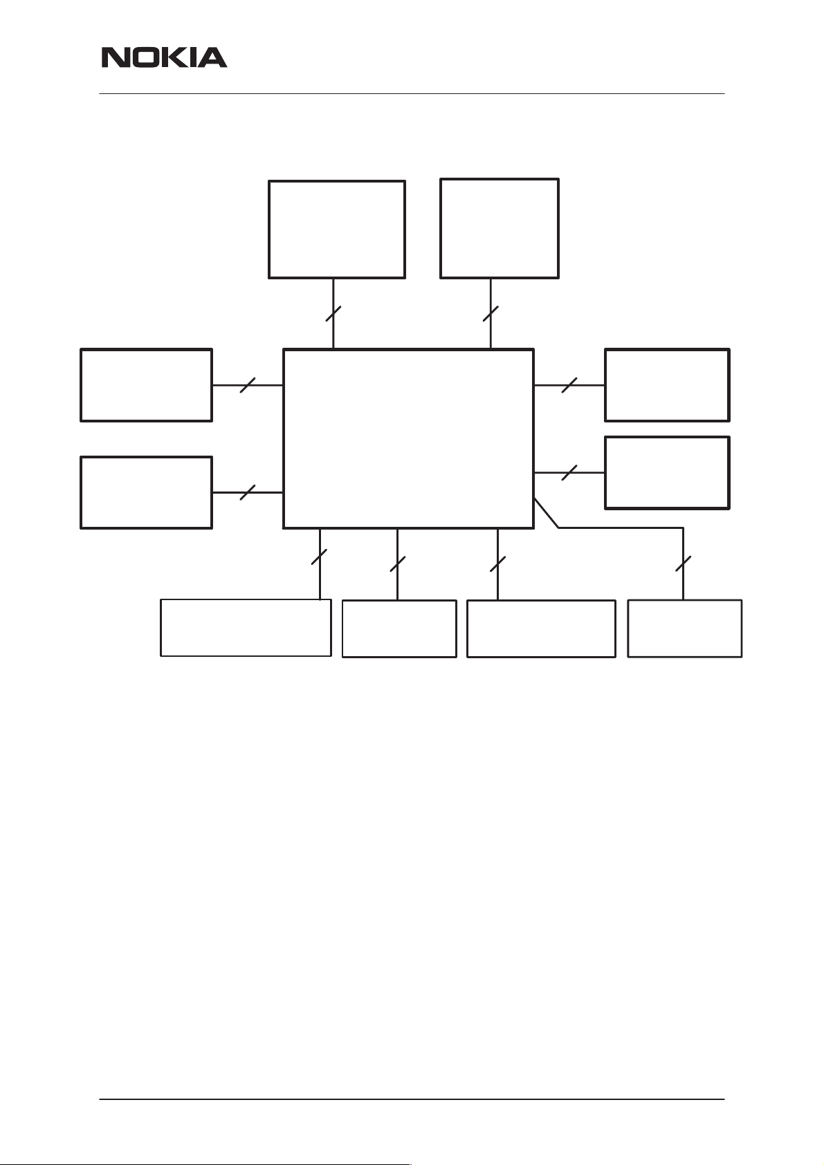
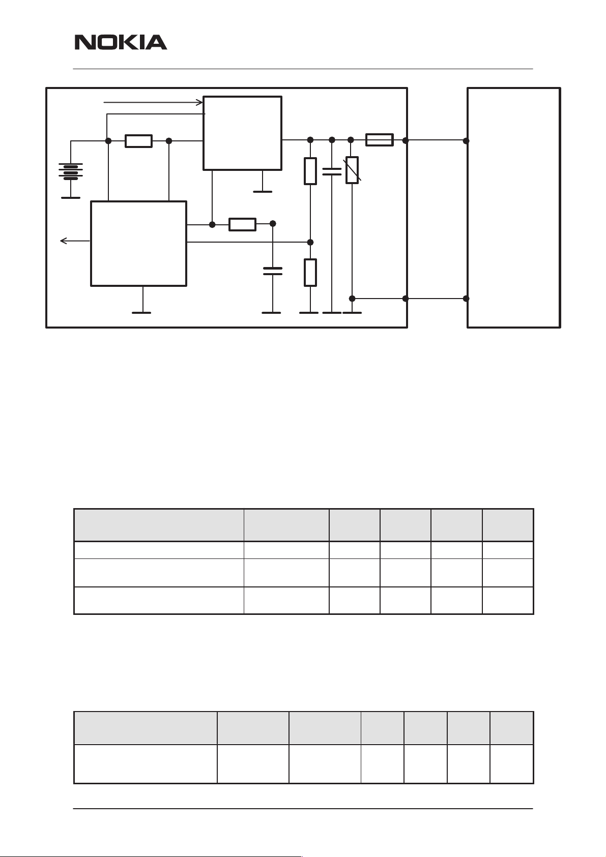
Interconnection Diagram
NSM–2
System Module
Keyboard
module
14
LCD
module
9
64
SIM Battery
Radio
Module
2+2
2
RM7
Charger
Antenna
2
3
2
4
Slide (mic.)
IR Link
Earpiece
HF/HS
Issue 1 12/1999
Nokia Mobile Phones Ltd.
Page 7
Page 8
NSM–2
System Module
System Module
Baseband Module
The baseband architecture supports a power saving function called ”sleep
mode”. This sleep mode shuts off the VCTCXO, which is used as system
clock source for both RF and baseband. During the sleep mode the sys-
tem runs from a 32 kHz crystal. The phone is waken up by a timer run-
ning from this 32 kHz clock supply. The sleeping time is determined by
some network parameters. The sleep mode is entered when both the
MCU and the DSP are in standby mode and the normal VCTCXO clock
has been switched off.
The battery charging is controlled by a PWM signal from the CCONT. The
PWM duty cycle is determined by a charging software and is fed to the
CHAPS charging switch.
PAMS Technical Documentation
Standard chargers (two wires) provide coarse supply power, which is
switched by the CHAPS for suitable charging voltage and current. Ad-
vanced chargers (three wires) are equipped with a control input. Three
wire chargers are treated like two wire ones.
Block Diagram
TX/RX SIGNALS
UI
IR
COBBA SUPPLY
COBBA
MAD
+
MEMORIES
RF SUPPLIES
CCONT
BB SUPPLY
CHAPS
PA SUPPL Y
32kHz
CLK
SLEEP CLOCK
SIM
VBAT
13MHz
CLK
SYSTEM CLOCK
BATTERY
Page 8
BASEBAND
EXT. AUDIO
HS–connector
Charger
connector
Nokia Mobile Phones Ltd.
Issue 1 12/1999
Page 9

PAMS Technical Documentation
Technical Summary
The baseband module consists four ASICs; CHAPS, CCONT, COBBA–
GJP and MAD2WD1, which take care of the baseband functions of the
engine.
The baseband is running from a 2.8V power rail, which is supplied by a
power controlling ASIC CCONT. In the CCONT there are 6 individually
controlled regulator outputs for RF–section and two outputs for the base-
band. In addition there is one +5V power supply output (V5V). The
CCONT contains also a SIM interface, which supports both 3V and 5V
SIM–cards. A real time clock function is integrated into the CCONT, which
utilizes the same 32kHz clock supply as the sleep clock. A backup power
supply is provided for the RTC, which keeps the real time clock running
when the main battery is removed. The backup power supply is a re-
chargable battery. The backup time with the battery is ten minutes mini-
mum.
The interface between the baseband and the RF section is mainly han-
dled by a COBBA ASIC. COBBA provides A/D and D/A conversion of the
in–phase and quadrature receive and transmit signal paths and also A/D
and D/A conversions of received and transmitted audio signals to and
from the user interface. The COBBA supplies the analog TXC and AFC
signals to RF section according to the MAD DSP digital control. Data
transmission between the COBBA and the MAD is implemented using se-
rial bus for high speed signalling and for PCM coded audio signals. Digital
speech processing is handled by the MAD ASIC. COBBA is a dual volt-
age circuit, the digital parts are running from the baseband supply VBB
and the analog parts are running from the analog supply VCOBBA.
NSM–2
System Module
The baseband supports both internal and external microphone inputs and
speaker outputs. Input and output signal source selection and gain control
is done by the COBBA according to control messages from the MAD.
Keypad tones, DTMF, and other audio tones are generated and encoded
by the MAD and transmitted to the COBBA for decoding. A buzzer and an
external vibra alert control signals are generated by the MAD with sepa-
rate PWM outputs.
EMC shieding is implemented using a metallized plastic frame. On the
other side the engine is shielded with PCB grounding. Heat generated by
the circuitry will be conducted out via the PCB ground planes.
Issue 1 12/1999
Nokia Mobile Phones Ltd.
Page 9
Page 10

NSM–2
System Module
PAMS Technical Documentation
External and Internal Signals and Connections
This section describes the external electrical connection and interface lev-
els on the baseband. The electrical interface specifications are collected
into tables that covers a connector or a defined interface.
DC (charger) connector
DC (charger) connector is physically integrated in the same component
with the accessory interface connector. DC connector has both jack and
contact pads for desk stand.
Service connector
Name Parameter Min Typ Max Unit Remark
MBUS Serial clock
from the
Prommer
FBUS_RX Serial data
from the
Prommer
FBUS_TX Data ac-
knowledge to
the Prommer
GND GND 0 0 V Ground
0
2.0
0
2.0
0
2.0
logic low
logic low
logic low
logic high
logic low
logic high
0.8
2.85
0.8
2.85
0.5
2.85
V Prommer detection and Seri-
al Clock for synchronous
communication
V Receive Data from
Prommer to Baseband
V Transmit Data from Base-
band to Prommer
The service connector is used as a flash programming interface for updating (i.e. re–programming) the flash program memory and an electrical
access for services to the engine.
When the flash prommer is connected to the phone supply power is provided through the battery contacts and the phone is powered up with a
pulse given to the BTEMP line.
Battery connector
The BSI contact on the battery connector is used to detect when the battery is to be removed to be able to shut down the operations of the SIM
card before the power is lost if the battery is removed with power on. The
BSI contact disconnects earlier than the supply power contacts to give
enough time for the SIM and LCD shut down.
Name Min Typ Max Unit Notes
VBATT 3.0 3.9 4.2 V Battery voltage
BSI
Page 10
0 2.85 V Battery size indication
Phone has 100kohm pull up resistor.
SIM Card removal detection
(Treshold is 2.4V@VBB=2.8V)
67 68 69 kohm Battery indication resistor (BLB–2)
22 kohm Battery indication resistor (service battery)
Nokia Mobile Phones Ltd.
Issue 1 12/1999
Page 11
PAMS Technical Documentation
NSM–2
System Module
NotesUnitMaxTypMinName
BTEMP
BGND 0 0 V Battery ground
0 1.4 V Battery temperature indication
Phone has a 100k (+–5%) pullup resistor,
Battery package has a NTC pulldown resistor:
47k+–5%@+25C , B=4050+–3%
2.1
5 10
1.9
90 100
0 1 kohm Local mode initialization (in production)
3
20
2.85
200
V
ms
V
ms
Phone power up by battery (input)
Power up pulse width
Battery power up by phone (output)
Power up pulse width
SIM card connector
The SIM card connector is located on the engine board beside the battery
pack.
Pin Name Parameter Min Typ Max Unit Notes
4 GND GND 0 0 V Ground
3, 5 VSIM 5V SIM Card
3V SIM Card
6 DATA 5V Vin/Vout
3V Vin/Vout
2 SIMRST 5V SIM Card
3V SIM Card
4.8
2.8
4.0
0
2.8
0
4.0
2.8
5.0
3.0
”1”
”0”
”1”
”0”
”1”
”1”
5.2
3.2
VSIM
0.5
VSIM
0.5
VSIM
VSIM
V Supply voltage
V SIM data
Trise/Tfall max 1us
V SIM reset
1 SIMCLK Frequency
Trise/Tfall
3.25
25
MHz
ns
SIM clock
RTC backup battery
The RTC block in CCONT needs a power backup to keep the clock running when the phone battery is disconnected. The backup power is supplied from a rechargable polyacene battery that can keep the clock running ten minutes minimum. The backup battery is charged from the main
battery through CHAPS.
Signal Parameter Min Typ Max Unit Notes
VBACK
VBACK
Backup battery charging from CHAPS
Backup battery charging from CHAPS
Backup battery supply
to CCONT
Backup battery supply
to CCONT
3.02 3.15 3.28 V
100 200 500 uA Vout@VBAT–0.2V
2 3.28 V
80 uA
Issue 1 12/1999
Nokia Mobile Phones Ltd.
Page 11
Page 12
NSM–2
System Module
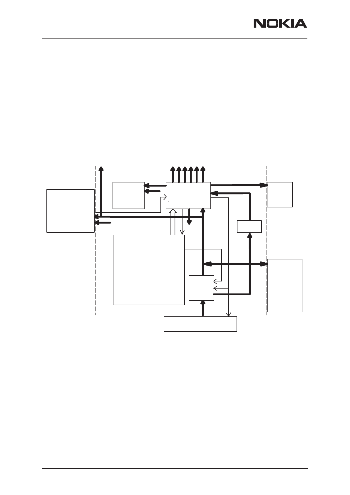
Power Distribution
In normal operation the baseband is powered from the phone‘s battery.
The battery consists of one Lithium–Ion cell. An external charger can be
used for recharging the battery and supplying power to the phone.
The baseband contains parts that control power distribution to whole
phone excluding those parts that use continuous battery supply. The battery feeds power directly to the CCONT and UI (buzzer and display and
keyboard lights).
The power management circuit CHAPS provides protection against overvoltages, charger failures and pirate chargers etc. that would otherwise
cause damage to the phone.
PAMS Technical Documentation
PA SUPPL Y
VCOBBA
COBBA
UI
VBAT
VBB
BASEBAND
VBB
MAD
+
MEMORIES
RF SUPPLIES
CCONT
PWRONX
CNTVR
CHARGER CONNECTOR
PWM
VBB
PURX
LIM
CHAPS
VIN
VSIM
SIM
RTC
BACKUP
VBAT
BATTERY
Battery charging
The electrical specifications give the idle voltages produced by the acceptable chargers at the DC connector input. The absolute maximum input voltage is 30V due to the transient suppressor that is protecting the
charger input. At phone end there is no difference between a plug–in
charger or a desktop charger. The DC–jack pins and bottom connector
charging pads are connected together inside the phone.
Page 12
Nokia Mobile Phones Ltd.
Issue 1 12/1999
Page 13
PAMS Technical Documentation
NSM–2
System Module
MAD
VBAT
MAD
CCONTINT
CCONT
Startup Charging
LIM
0R22
PWM_OUT
GND
ICHAR
VCHAR
VOUT
CHAPS
RSENSE
PWM
22k
VCH
GND
1n
TRANSCEIVER
1u
100k
10k
30V
2A
VIN
L_GND
CHARGER
When a charger is connected, the CHAPS is supplying a startup current
minimum of 130mA to the phone. The startup current provides initial
charging to a phone with an empty battery. Startup circuit charges the
battery until the battery voltage level is reaches 3.0V (+/– 0.1V) and the
CCONT releases the PURX reset signal and program execution starts.
Charging mode is changed from startup charging to PWM charging that is
controlled by the MCU software. If the battery voltage reaches 3.55V
(3.75V maximum) before the program has taken control over the charging, the startup current is switched off. The startup current is switched on
again when the battery voltage is sunken 100mV (nominal).
Parameter Symbol Min Typ Max Unit
VOUT Start– up mode cutoff limit Vstart 3.45 3.55 3.75 V
VOUT Start– up mode hysteresis
NOTE: Cout = 4.7 uF
Start–up regulator output current
VOUT = 0V ... Vstart
Vstarthys 80 100 200 mV
Istart 130 165 200 mA
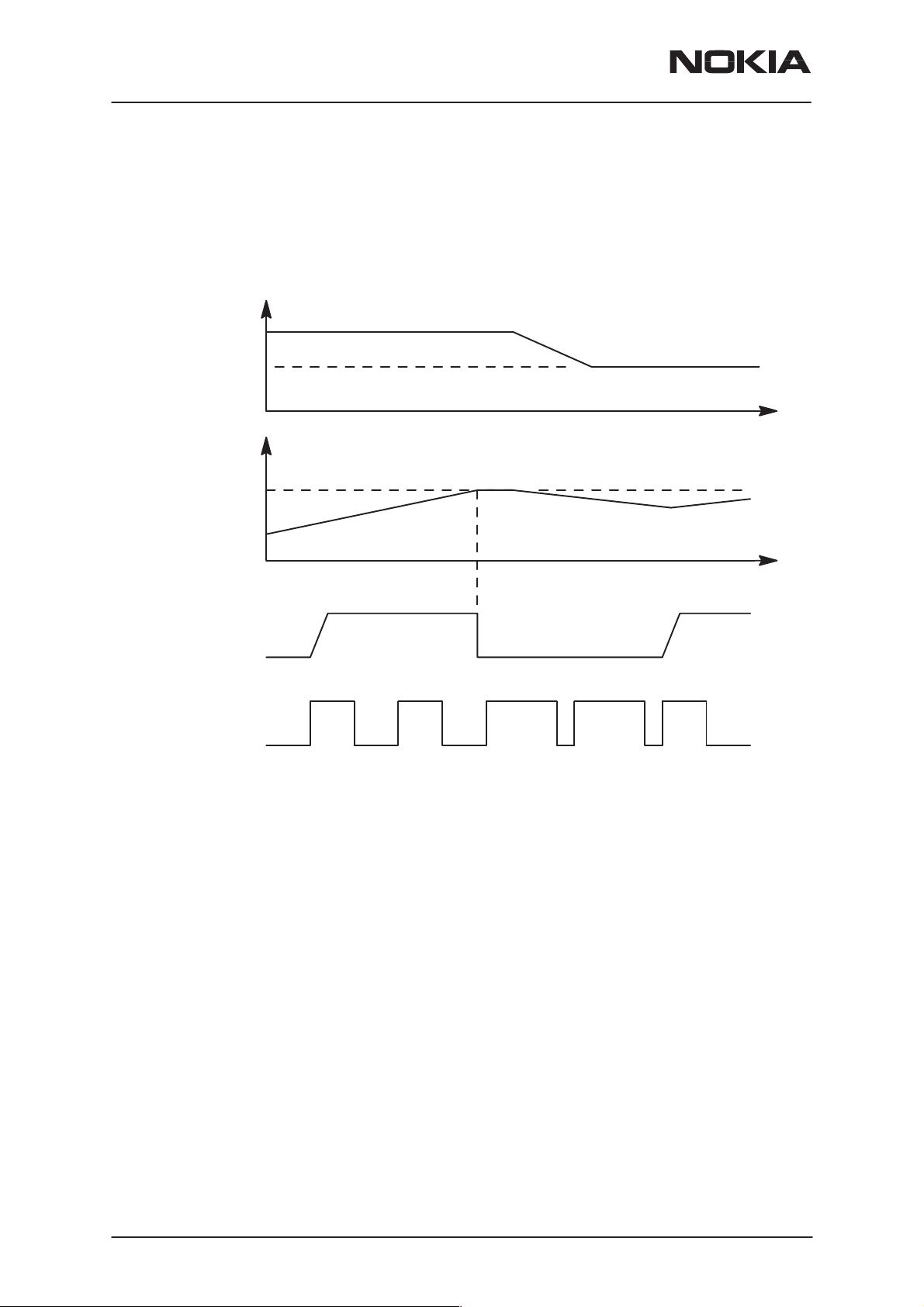
Battery Overvoltage Protection
Output overvoltage protection is used to protect phone from damage.
This function is also used to define the protection cutoff voltage for different battery types (Li or Ni). The power switch is immediately turned OFF if
the voltage in VOUT rises above the selected limit VLIM1 or VLIM2.
Parameter Symbol LIM input Min Typ Max Unit
Output voltage cutoff limit
(during transmission or Li–
battery)
VLIM LOW 4.4 4.6 4.8 V
Issue 1 12/1999
Nokia Mobile Phones Ltd.
Page 13
Page 14
NSM–2
System Module
The voltage limit (VLIM1 or VLIM2) is selected by logic LOW or logic
HIGH on the CHAPS (N101) VLIM input pin. In NSM–2 VLIM is fixed low
in HW.
When the switch in output overvoltage situation has once turned OFF, it
stays OFF until the the battery voltage falls below VLIM and PWM = LOW
is detected. The switch can be turned on again by setting PWM = HIGH.
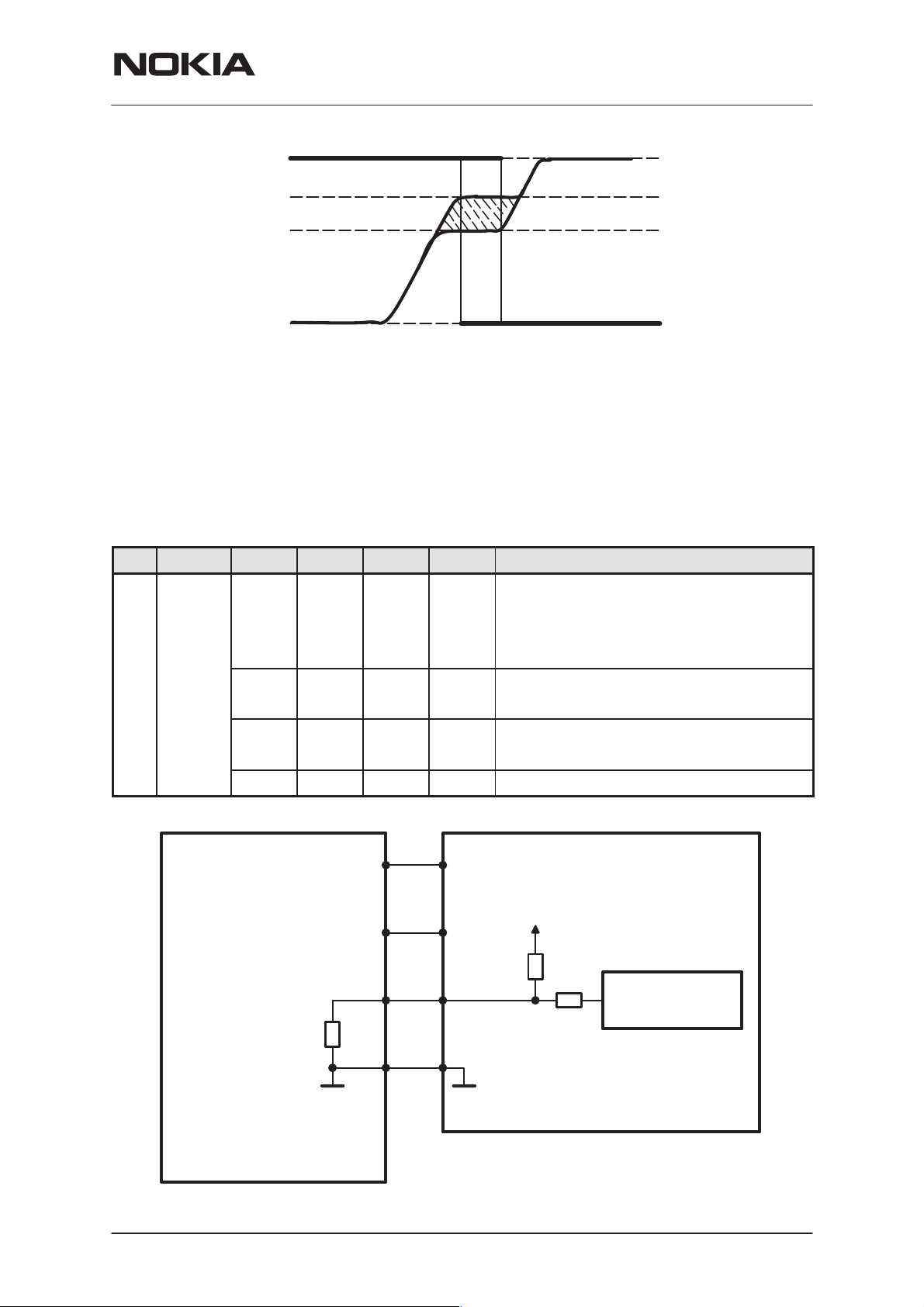
VCH
VCH<VOUT
VOUT
VLIM
PAMS Technical Documentation
t
SWITCH
PWM (1 Hz)
ON OFF
t
ON
Page 14
Nokia Mobile Phones Ltd.
Issue 1 12/1999
Page 15
PAMS Technical Documentation
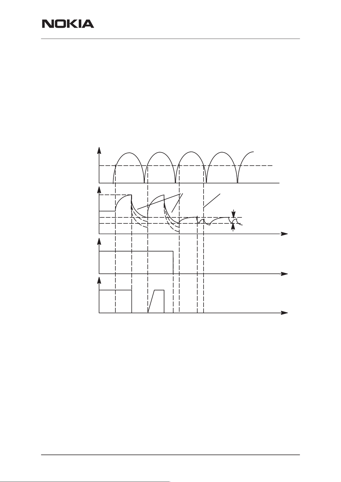
Battery Removal During Charging
Output overvoltage protection is also needed in case the main battery is
removed when charger connected or charger is connected before the battery is connected to the phone.
With a charger connected, if VOUT exceeds VLIM, CHAPS turns switch
OFF until the charger input has sunken below Vpor (nominal 3.0V, maximum 3.4V). MCU software will stop the charging (turn off PWM) when it
detects that battery has been removed. The CHAPS remains in protection
state as long as PWM stays HIGH after the output overvoltage situation
has occured.
NSM–2
System Module
VCH
(Standard
Charger)
VOUT
PWM
SWITCH
Vpor
VLIM
4V
Vstart
”1”
”0”
ON
OFF
Droop depends on load
& C in phone
2
5
4
6
7
Istart off due to VCH<Vpor
Vstarthys
t
t
t
1.1Battery removed, (standard) charger connected, VOUT rises (follows charger voltage)
2. VOUT exceeds limit VLIM(X), switch is turned immediately OFF
3.3VOUT falls (because no battery) , also VCH<Vpor (standard chargers full–rectified
output). When VCH > Vpor and VOUT < VLIM(X) –> switch turned on again (also PWM
is still HIGH) and VOUT again exceeds VLIM(X).
4. Software sets PWM = LOW –> CHAPS does not enter PWM mode
5. PWM low –> Startup mode, startup current flows until Vstart limit reached
6. VOUT exceeds limit Vstart, Istart is turned off
7. VCH falls below Vpor
Issue 1 12/1999
Nokia Mobile Phones Ltd.
Page 15
Page 16
NSM–2
System Module
PAMS Technical Documentation
PWM
When a charger is used, the power switch is turned ON and OFF by the
PWM input. PWM rate is 1Hz. When PWM is HIGH, the switch is ON and
the output current Iout = charger current – CHAPS supply current. When
PWM is LOW, the switch is OFF and the output current Iout = 0. To prevent the switching transients inducing noise in audio circuitry of the phone
soft switching is used.
Battery Identification
Different battery types are identified by a pulldown resistor inside the battery pack. The BSI line inside transceiver has a 100k pullup to VBB. The
MCU can identify the battery by reading the BSI line DC–voltage level
with a CCONT (N100) A/D–converter.
Name Min Typ Max Unit Notes
BSI
0 2.8 V Battery size indication
100k pullup resistor to VBB in phone
SIM Card removal detection
(Treshold is 2.4V@VBB=2.8V)
67 68 69 kohm Indication of a BLB–2 battery (650 mAh Li–Ion)
22 kohm Indication resistor for a service battery
VBATT
BATTERY
BTEMP
BSI
R
s
BGND
2.8V
100k
10n
10k
TRANSCEIVER
BSI
SIMCardDetX
CCONT
MAD
Page 16
The battery identification line is used also for battery removal detection.
The BSI line is connected to a SIMCardDetX line of MAD2. SIMCardDetX
is a threshold detector with a nominal input switching level 0.85xVcc for a
rising edge and 0.55xVcc for a falling edge. The battery removal detection
is used as a trigger to power down the SIM card before the power is lost.
The BSI contact in the battery contact disconnects before the other contacts so that there is a delay between battery removal detection and supply power off.
Nokia Mobile Phones Ltd.
Issue 1 12/1999
Page 17
PAMS Technical Documentation
Vcc
0.850.05 Vcc
0.550.05 Vcc
SIMCARDDETX
GND
Battery Temperature
The battery temperature is measured with a NTC inside the battery pack.
The BTEMP line inside transceiver has a 100k pullup to VREF. The MCU
can calculate the battery temperature by reading the BTEMP line DC–
voltage level with a CCONT (N100) A/D–converter.
NSM–2
System Module
S
IGOUT
Pin Name Min Typ Max Unit Notes
3 BTEMP
0 1.4 V Battery temperature indication
100k pullup resistor to VREF in phone
Battery package has NTC pull down resis-
tor:
47k +/–5%@+25C , B=4050+/–3%
2.1
5 10
1.9
90
–5 5 % 100k pullup resistor tolerance
100
BATTERY
3
20
2.8
200
VBATT
BSI
BTEMP
V
ms
V
ms
Phone power up by battery (input)
Power up pulse width
Battery power up by phone (output)
Power up pulse width
TRANSCEIVER
VREF
100k
10k
BTEMP
CCONT
Issue 1 12/1999
R
NTC
T
BGND
Nokia Mobile Phones Ltd.
Page 17
Page 18

NSM–2
System Module
Supply Voltage Regulators
The heart of the power distrubution is the CCONT. It includes all the voltage regulators and feeds the power to the whole system. The baseband
digital parts are powered from the VBB regulator which provides 2.8V
baseband supply. The baseband regulator is active always when the
phone is powered on. The VBB baseband regulator feeds MAD and memories, COBBA digital parts and the LCD driver in the UI section. There is
a separate regulator for a SIM card. The regulator is selectable between
3V and 5V and controlled by the SIMPwr line from MAD to CCONT. The
COBBA analog parts are powered from a dedicated 2.8V supply VCOBBA. The CCONT supplies also 5V for RF and for flash VPP. The CCONT
contains a real time clock function, which is powered from a RTC backup
when the main battery is disconnected. The RTC backup is rechargable
polyacene battery. The battery is charged from the main battery voltage
by the CHAPS when the main battery voltage is over 3.2V.
PAMS Technical Documentation
Operating mode
Vref
RF REG VCOBBA VBB VSIM SIMIF
Power off Off Off Off Off Off Pull
down
Power on On On/Off On On On On/Off
Reset On Off
VR1 On
On On Off Pull
down
Sleep On Off Off On On On/Off
NOTE: COBBA regulator is off in SLEEP mode. Its output pin may be fed
from VBB in SLEEP mode by setting bit RFReg(5) to ’1’ (default).
CCONT includes also five additional 2.8V regulators providing power to
the RF section. These regulators can be controlled either by the direct
control signals from MAD or by the RF regulator control register in
CCONT which MAD can update. Below are the listed the MAD control
lines and the regulators they are controlling.
– TxPwr controls VTX regulator (VR5)
– RxPwr controls VRX regulator (VR2)
Page 18
– SynthPwr controls all the rf regulators except VR1
– VCXOPwr controls VXO regulator (VR1)
In additon to the above mentioned signals MAD includes also TXP control
signal which goes to HAGAR power control block. The transmitter power
control TXC is led from COBBA to HAGAR.
Nokia Mobile Phones Ltd.
Issue 1 12/1999
Page 19

PAMS Technical Documentation
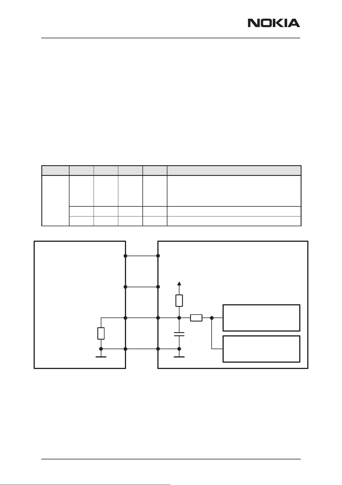
Switched Mode Supply VSIM
There is a switched mode supply for SIM–interface. SIM voltage is selected via serial IO. The 5V SMR can be switched on independently of the
SIM voltage selection, but can’t be switched off when VSIM voltage value
is set to 5V.
NOTE: VSIM and V5V can give together a total of 30mA.
In the next figure the principle of the SMR / VSIM–functions is shown.
CCONT External
VBAT
NSM–2
System Module
V5V_4
V5V_3
V5V_2
VSIM
5V reg
Power Up and Power Down
The baseband is powered up by:
1. Pressing the power key, that generates a PWRONX interrupt
signal from the power key to the CCONT, which starts the power up procedure.
2. Connecting a charger to the phone. The CCONT recognizes
the charger from the VCHAR voltage and starts the power up
procedure.
3. A RTC interrupt. If the real time clock is set to alarm and the
phone is switched off, the RTC generates an interrupt signal,
when the alarm is gone off. The RTC interrupt signal is connected to the PWRONX line to give a power on signal to the
CCONT just like the power key.
V5V
5V
5/3V
4. A battery interrupt. Intelligent battery packs have a possibility
to power up the phone. When the battery gives a short (10ms)
voltage pulse through the BTEMP pin, the CCONT wakes up
and starts the power on procedure.
Power up with a charger
When the charger is connected CCONT will switch on the CCONT digital
voltage as soon as the battery voltage exceeds 3.0V. The reset for
Issue 1 12/1999
Nokia Mobile Phones Ltd.
Page 19
Page 20

NSM–2
System Module
CCONT’s digital parts is released when the operating voltage is stabilized
( 50 us from switching on the voltages). Operating voltage for VCXO is
also switched on. The counter in CCONT digital section will keep MAD in
reset for 62 ms (PURX) to make sure that the clock provided by VCXO is
stable. After this delay MAD reset is relased, and VCXO –control
(SLEEPX) is given to MAD. The next diagram explains the power on procedure with charger ( the picture assumes empty battery, but the situation
would be the same with full battery):
PAMS Technical Documentation
SLEEPX
PURX
CCPURX
12 3
1: Battery voltage over 3.0==>Digital voltages to CCONT (VBB)
2: CCONT digital reset released. VCXO turned on
3: 62ms delay before PURX released
When the phone is powered up with an empty battery pack using the
standard charger, the charger may not supply enough current for standard powerup procedure and the powerup must be delayed.
Power Up With The Power Switch (PWRONX)
When the power on switch is pressed the PWRONX signal will go low.
CCONT will switch on the CCONT digital section and VCXO as was the
case with the charger driven power up. If PWRONX is low when the 64
ms delay expires, PURX is released and SLEEPX control goes to MAD. If
PWRONX is not low when 64 ms expires, PURX will not be released, and
CCONT will go to power off ( digital section will send power off signal to
analog parts)
Vbat
VR6
VR1
VBB (2.8V)
Vchar
Vref
Page 20
Nokia Mobile Phones Ltd.
Issue 1 12/1999
Page 21

PAMS Technical Documentation
12 3
1:Power switch pressed ==> Digital voltages on in CCONT (VBB)
2: CCONT digital reset released. VCXO turned on
3: 62 ms delay to see if power switch is still pressed.
NSM–2
System Module
SLEEPX
PURX
CCPURX
PWRONX
VR1,VR6
VBB (2.8V)
Vchar
Power Up by RTC
RTC (internal in CCONT) can power the phone up by changing RTCPwr
to logical 1.
Power Up by IBI
IBI can power CCONT up by giving a short pulse (10ms) through the
BTEMP line. After powerup BTEMP will act as any other input channel for
ADC.
When the PURX reset is released, the MAD releases the system reset
ExtSysResetX and the internal MCUResetX signals and starts the boot
program execution from MAD bootrom if MAD GenSDIO pin is pulled low
or from external memory if GenSDIO pin is pulled high. In normal operation the program execution continues from the flash program memory. If
the MBUS line is pulled low during the power up the bootrom starts a
flash programming sequence and waits for the prommer response
through FBUS_RX line.
Power Down
The baseband is powered down by:
Issue 1 12/1999
1. Pressing the power key, that is monitored by the MAD, which
starts the power down procedure.
2. If the battery voltage is dropped below the operation limit, either by not charging it or by removing the battery.
3. Letting the CCONT watchdog expire, which switches off all
CCONT regulators and the phone is powered down.
Nokia Mobile Phones Ltd.
Page 21
Page 22

NSM–2
System Module
4. Setting the real time clock to power off the phone by a timer.
The RTC generates an interrupt signal, when the alarm is gone
off. The RTC interrupt signal is connected to the PWRONX line
to give a power off signal to the CCONT just like the power key.
The power down is controlled by the MAD. When the power key has been
pressed long enough or the battery voltage is dropped below the limit the
MCU initiates a power down procedure and disconnects the SIM power.
Then the MCU outputs a system reset signal and resets the DSP. If there
is no charger connected the MCU writes a short delay to CCONT watchdog and resets itself. After the set delay the CCONT watchdog expires,
which activates the PURX and all regulators are switched off and the
phone is powered down by the CCONT.
If a charger is connected when the power key is pressed the phone enters into the acting dead mode.
Modes of Operation
PAMS Technical Documentation
Acting Dead
If the phone is off when the charger is connected, the phone is powered
on but enters a state called ”acting dead”. To the user the phone acts as if
it was switched off. A battery charging alert is given and/or a battery
charging indication on the display is shown to acknowledge the user that
the battery is being charged.
Active Mode
In the active mode the phone is in normal operation, scanning for channels, listening to a base station, transmitting and processing information.
All the CCONT regulators are operating. There are several substates in
the active mode depending on if the phone is in burst reception, burst
transmission, if DSP is working etc.
Sleep Mode
In the sleep mode all the regulators except the baseband VBB and the
SIM card VSIM regulators are off. Sleep mode is activated by the MAD
after MCU and DSP clocks have been switched off. The voltage regulators for the RF section are switched off and the VCXO power control,
VCXOPwr is set low. In this state only the 32 kHz sleep clock oscillator in
CCONT is running. The flash memory power down input is connected to
the ExtSysResetX signal, and the flash is deep powered down during the
sleep mode.
Page 22
The sleep mode is exited either by the expiration of a sleep clock counter
in the MAD or by some external interrupt, generated by a charger connection, key press, headset connection etc. The MAD starts the wake up
sequence and sets the VCXOPwr and ExtSysResetX control high. After
VCXO settling time other regulators and clocks are enabled for active
mode.
Nokia Mobile Phones Ltd.
Issue 1 12/1999
Page 23

PAMS Technical Documentation
If the battery pack is disconnect during the sleep mode, the CCONT pulls
the SIM interface lines low as there is no time to wake up the MCU.
Charging
Charging can be performed in any operating mode.The battery type/size
is indicated by a resistor inside the battery pack. The resistor value corresponds to a specific battery capacity. This capacity value is related to the
battery technology as different capacity values are achieved by using different battery technology.
The battery voltage, temperature, size and current are measured by the
CCONT controlled by the charging software running in the MAD.
The power management circuitry controls the charging current delivered
from the charger to the battery. Charging is controlled with a PWM input
signal, generated by the CCONT. The PWM pulse width is controlled by
the MAD and sent to the CCONT through a serial data bus. The battery
voltage rise is limited by turning the CHAPS switch off when the battery
voltage has reached 4.2 V. Charging current is monitored by measuring
the voltage drop across a 220 mohm resistor.
NSM–2
System Module
Watchdog
The Watchdog block inside CCONT contains a watchdog counter and
some additional logic which are used for controlling the power on and
power off procedures of CCONT. Watchdog output is disabled when
WDDisX pin is tied low. The WD-counter runs during that time, though.
Watchdog counter is reset internally to 32 s at power up. Normally it is reset by MAD writing a control word to the WDReg.
Issue 1 12/1999
Nokia Mobile Phones Ltd.
Page 23
Page 24

NSM–2
System Module
Audio control
PCM serial interface
The interface consists of following signals: a PCM codec master clock
(PCMDClk), a frame synchronization signal to DSP (PCMSClk), a codec
transmit data line (PCMTX) and a codec receive data line (PCMRX). The
COBBA–GJP generates the PCMDClk clock, which is supplied to DSP
SIO. The COBBA–GJP also generates the PCMSClk signal to DSP by dividing the PCMDClk. The PCMDClk frequency is 1.000 MHz and is generated by dividing the RFIClk 13 MHz by 13. The COBBA–GJP further divides the PCMDClk by 125 to get a PCMSClk signal, 8.0 kHz.
PCMDClk
PCMSClk
PAMS Technical Documentation
PCMTxData
PCMRxData
sign extended
MSB
15 14 13 12 011 10
sign extended
MSB
LSB
LSB
Page 24
Nokia Mobile Phones Ltd.
Issue 1 12/1999
Page 25

PAMS Technical Documentation
Digital Control
The baseband functions are controlled by the MAD asic, which consists of
a MCU, a system ASIC and a DSP.
MAD2 WD1
MAD2 WD1 contains following building blocks:
– ARM RISC processor with both 16–bit instruction set (THUMB mode)
and 32–bit instruction set (ARM mode)
– TI Lead DSP core with peripherials:
– API (Arm Port Interface memory) for MCU–DSP commu-
nication, DSP code download, MCU interrupt handling vec-
tors (in DSP RAM) and DSP booting.
– Serial port (connection to PCM)
– Timer
NSM–2
System Module
– DSP memory
– BUSC (BusController for controlling accesses from ARM to API, Sys-
tem Logic and MCU external memories, both 8– and 16–bit memories)
– System Logic
– CTSI (Clock, Timing, Sleep and Interrupt control)
– MCUIF (Interface to ARM via B
USC). Contains MCU Boo-
tROM
– DSPIF (Interface to DSP)
– MFI (Interface to COBBA AD/DA Converters)
– CODER (Block encoding/decoding and A51&A52 ciphering)
– AccIF(Accessory Interface)
– SCU (Synthesizer Control Unit for controlling 2 separate
synthesizer)
– UIF (Keyboard interface, serial control interface for COBBA
PCM Codec, LCD Driver and CCONT)
– SIMI (SimCard interface with enhanched features)
– PUP (Parallel IO, USART and PWM control unit for vibra
and buzzer)
The MAD2 operates from a 13 MHz system clock, which is generated
from the 13Mhz VCXO frequency. The MAD2 supplies a 6,5 MHz or a 13
MHz internal clock for the MCU and system logic blocks and a 13 MHz
clock for the DSP, where it is multiplied to 45.5 MHz DSP clock. The system clock can be stopped for a system sleep mode by disabling the
VCXO supply power from the CCONT regulator output. The CCONT provides a 32 kHz sleep clock for internal use and to the MAD2, which is
Issue 1 12/1999
– Flexpool
Nokia Mobile Phones Ltd.
Page 25
Page 26

NSM–2
System Module
used for the sleep mode timing. The sleep clock is active when there is a
battery voltage available i.e. always when the battery is connected.
PAMS Technical Documentation
Ball Name Pin
Type
A1 MCUGemIO 0 O 2 0 MCU General
C2
D2 Col4 I/O UIF 2 Input program-
D3 Col3 I/O UIF 2 Input program-
H11 MCUGenIO1 I/O 2 Input,
E4 GND Ground
D4 Col2 I/O UIF 2 Input program-
C4 Col1 I/O UIF 2 Input program-
C3 Col0 I/O UIF 2 Input program-
D1 LCDCSX I/O UIF 2 Input external
LEADGND
Connected
to/from
Drive
req.
mA
Reset
State
pullup
Note Explanation
purpose output
Lead Ground
I/O line for key-
mable pullup
PR0201
mable pullup
PR0201
pullup
PR0201
mable pullup
PR0201
mable pullup
PR0201
mable pullup
PR0201
pullup/down
board column 4
I/O line for keyboard column 3
General purpose
I/O port
I/O line for keyboard column 2
I/O line for keyboard column 1
I/O line for keyboard column 0
serial LCD driver
chip select, par-
allel LCD driver
enable
port
E1
F12
E3 Row5LCDCD I/O UIF 2 Input,
N4 VCC_CORE Core VCC in
E2 Row4 I/O UIF 2 Input,
F4 Row3 I/O UIF 2 Input,
Page 26
LEADVCC
LoByteSelX
pullup
pullup
pullup
Nokia Mobile Phones Ltd.
pullup
PR0201
3325c10
pullup
PR0201
pullup
PR0201
Lead Power
NC
Keyboard row5
data I/O , serial
LCD driver com-
mand/data indi-
cator, parallel
LCD driver read/
write select
Power
I/O line for key-
board row 4, par-
allel LCD driver
register selection
control
I/O line for key-
board row 3, par-
allel LCD driver
data
Issue 1 12/1999
Page 27

PAMS Technical Documentation
NSM–2
System Module
NameBall
F3 Row2 I/O UIF 2 Input,
F2 Row1 I/O UIF 2 Input,
F1 Row0 I/O UIF 2 Input,
L11 JTDO O 2 Tri–
L5 GND Ground
N12 JTRst I Input,
M12 JTClk I Input pulldown
N13 JTDI I Input,
M13 JTMS I Input,
G13 VCC_IO IO VCC in
L12 CoEmu0 I/O 2 Input,
L13 CoEmu1 I/O 2 Input,
H4
LEADGND
Pin
Type
Connected
to/from
Drive
req.
mA
State
pullup
pullup
pullup
state
pull-
down
pullup
pullup
pullup
pullup
pullup
PR0201
pullup
PR0201
pullup
PR0201
pulldown
PD0201
PD0201
pullup
PR0201
pullup
PR0201
3325c10
pullup
PR0201
pullup
PR0201
ExplanationNoteReset
I/O line for key-
board row 2, par-
allel LCD driver
data
I/O line for key-
board row 1, par-
allel LCD driver
data
I/O line for key-
board row 0, par-
allel LCD driver
data
JTAG data out
JTAG reset
JT AG Clock
JTAG data in
JTAG mode se-
lect
Power
DSP/MCU
emulation port 0
DSP/MCU
emulation port 1
Lead Ground
L1
N3 MCUAd0 O MCU
K4
N2 MCUAd1 O MCU
N1 MCUAd2 O MCU
M4 MCUAd3 O MCU
M3 MCUAd4 O MCU
M2 MCUAd5 O MCU
M1 MCUAd6 O MCU
Issue 1 12/1999
ARMGND
MEMORY
ARMVCC
MEMORY
MEMORY
MEMORY
MEMORY
MEMORY
MEMORY
Nokia Mobile Phones Ltd.
ARM Ground
2 0 MCU address
bus
ARM Power
2 0 MCU address
bus
2 0 MCU address
bus
2 0 MCU address
bus
2 0 MCU address
bus
2 0 MCU address
bus
2 0 MCU address
bus
Page 27
Page 28
NSM–2
System Module
PAMS Technical Documentation
NameBall
H1 VCC_IO IO VCC in
L4 MCUAd7 O MCU
L3 MCUAd8 O MCU
L2 MCUAd9 O MCU
K5 MCUAd10 O MCU
J4 GND Ground
K3 MCUAd11 O MCU
K2 MCUAd12 O MCU
K1 MCUAd13 O MCU
J3 MCUAd14 O MCU
Pin
Type
Connected
to/from
MEMORY
MEMORY
MEMORY
MEMORY
MEMORY
MEMORY
MEMORY
MEMORY
Drive
req.
mA
State
3325c10
2 0 MCU address
2 0 MCU address
2 0 MCU address
2 0 MCU address
2 0 MCU address
2 0 MCU address
2 0 MCU address
2 0 MCU address
ExplanationNoteReset
Power
bus
bus
bus
bus
bus
bus
bus
bus
J2 MCUAd15 O MCU
MEMORY
J1 MCUAd16 O MCU
MEMORY
M10 VCC_CORE Core VCC in
H3 MCUAd17 O MCU
MEMORY
H2 MCUAd18 O MCU
MEMORY
G4 MCUAd19 O MCU
MEMORY
G3 MCUAd20 O MCU
MEMORY
G2 VCONT O
K6 ExtMCUDa0 I/O MCU
MEMORY
K9 GND Ground
L6 ExtMCUDa1 I/O MCU
MEMORY
M6 ExtMCUDa2 I/O MCU
MEMORY
2 0 MCU address
bus
2 0 MCU address
bus
Power
3325c10
2 0 MCU address
bus
2 0 MCU address
bus
2 0 MCU address
bus
2 0 MCU address
bus
2 Input MCU data bus
2 Output MCU data bus
2 Output MCU data bus
N6 ExtMCUDa3 I/O MCU
MEMORY
L7 ExtMCUDa4 I/O MCU
MEMORY
Page 28
Nokia Mobile Phones Ltd.
2 Output MCU data bus
2 Output MCU data bus
Issue 1 12/1999
Page 29

PAMS Technical Documentation
NSM–2
System Module
NameBall
M7 ExtMCUDa5 I/O MCU
N7 ExtMCUDa6 I/O MCU
N8 ExtMCUDa7 I/O MCU
M8 MCUGenIODa0 I/O 2 Input MCU Data in
L8 MCUGenIODa1 I/O 2 Input MCU Data in
K8 MCUGenIODa2 I/O 2 Input MCU Data in
N9 MCUGenIODa3 I/O 2 Input MCU Data in
E10 GND Ground
M9 MCUGenIODa4 I/O 2 Input MCU Data in
L9 MCUGenIODa5 I/O 2 Input MCU Data in
Pin
Type
Connected
to/from
MEMORY
MEMORY
MEMORY
Drive
req.
mA
State
2 Output MCU data bus
2 Output MCU data bus
2 Output MCU data bus
16–bit mode
16–bit mode
16–bit mode
16–bit mode
16–bit mode
16–bit mode
ExplanationNoteReset
General purpose
I/O port
General purpose
I/O port
General purpose
I/O port
General purpose
I/O port
General purpose
I/O port
General purpose
I/O port
N10 MCUGenIODa6 I/O 2 Input MCU Data in
16–bit mode
L10 MCUGenIODa7 I/O 2 Input MCU Data in
16–bit mode
M5 MCURdX O MCU
MEMORY
G11 VCC_CORE Core VCC in
N5 MCUWrX O MCU
MEMORY
N11 ROM1SelX O MCU ROM 2 1 ROM chip select
M11 RAMSelX O MCU RAM 2 1 RAM chip select
J11 IRON O IR Mod 2 1 IR control
A1 MCUGenIO1 I/O 2 Input,
D8 DSPXF O 2 1 External flag
K10
K11 RFClk I VCXO Input System clock
SCVCC
2 1 MCU Read
3325c10
2 1 MCU write
pullup
pullup
PR0201
General purpose
I/O port
General purpose
I/O port
strobe
Power
strobe
General purpose
I/O port
Special cell Pow-
er
from VCTCXO
K12 RFClkGnd Input System clock
reference ground
input
K13 SIMCardDetX I Input SIM card detec-
tion
Issue 1 12/1999
Nokia Mobile Phones Ltd.
Page 29
Page 30

NSM–2
System Module
PAMS Technical Documentation
NameBall
J10
D9 BuzzPWM O BUZZER 2 0 Buzzer PWM
D11
G12 VibraPWM O VIBRA 2 0 Vibra PWM con-
C9 GND Ground
E12 MCUGenIO3 I/O 2 Input,
E13 MCUGenIO2 I/O 2 Input,
J13 KBLights O UIF 2 1
C5 AccTxData I/O 4 Tri–
B6 VCC_IO IO VCC in
F11 HookDet I Input Non–MBUS ac-
SCGND
LEADVCC
Pin
Type
Connected
to/from
Drive
req.
mA
State
pullup
pullup
State
pullup
PR1001
pullup
PR1001
external
pullup
3325c10
ExplanationNoteReset
Special cell
Ground
control
LEAD Power
trol
General purpose
I/O port
General purpose
I/O port
Accessory TX
data, Flash_TX
Power
cessory connec-
tion detector
F10 HeadDet I Input Headset detec-
tion interrupt
D6 AccRxData I Input Accessory RX
data, Flash_RX
D5 GND Ground
G10 MCUGenIO4 I/O 2 Input,
pull-
down
B5 MBUS I/O 2 Input,
exter-
nal
pullup
E11 VCXOPwr O CCONT 2 1 VCXO regulator
D13 SynthPwr O CCONT 2 0 Synthesizer reg-
B7 VCC_CORE Core VCC in
C10 GenCCONTCSX O CCONT 2 1 Chip select to
F13
LEADGND
pulldown
PD1001
external
pullup
3325c10
General purpose
I/O port
MBUS, Flash
clock
control
ulator control
Power
CCONT
LEAD Ground
B10 GenSDIO I/O CCONT, UIF 2 Input,
exter-
pullup/
down
Page 30
Nokia Mobile Phones Ltd.
nal
external
pullup/down
depending
on how to
boot
Serial data in/out
Issue 1 12/1999
Page 31

PAMS Technical Documentation
NSM–2
System Module
NameBall
A10 GenSClk O CCONT, UIF 2 0 Serial clock
C11 SIMCardData I/O CCONT 2 0 SIM data
J12 GND Ground
B13 PURX I CCONT Input Power Up Reset
B12 CCONTInt I CCONT Input CCONT interrupt
A13 Clk32k I CCONT Input Sleep clock os-
D10 VCC_IO IO VCC in
A12 SIMCardClk O CCONT 2 0 SIM clock
B11 SIMCardRstX O CCONT 2 0 SIM reset
A11 SIMCardIOC O CCONT 2 0 SIM data in/out
D12 SIMCardPwr O CCONT 2 0 SIM power con-
H10
LEADVCC
Pin
Type
Connected
to/from
Drive
req.
mA
State
3325c10
ExplanationNoteReset
cillator input
Power
control
trol
LEAD Power
C13 RxPwr O 2 0 (RX regulator
control)
C12 TxPwr O 2 0 (TX regulator
control)
H12 TestMode I Input,
pull-
down
H13 ExtSysResetX O 2 0 System Reset
B9 PCMTxData O COBBA 2 0 Transmit data,
K7 VCC_IO IO VCC in
A9 PCMRxData I COBBA Input Receive data,
B8 PCMDClk I COBBA Input Transmit clock,
A8 PCMSClk I COBBA Input Transmitframe
C6 COBBAClk O COBBA 4 1 COBBA clock,
A6 COBBACSX COBBA COBBA
pulldown
PD0201
3325c10
Test mode select
DX
Power
RX
CLKX
sync, FSX
13 MHz
A7 COBBASD COBBA COBBA
C7 IData COBBA COBBA
D7 QData COBBA COBBA
G1 VCC_CORE Core VCC in
3325c10
Issue 1 12/1999
Nokia Mobile Phones Ltd.
Power
Page 31
Page 32

NSM–2
System Module
PAMS Technical Documentation
NameBall
C1 DSPGenOut3 O RF 2 0 DSP general
B4 DSPGenOut2 O RF 2 0 DSP general
A4 DSPGenOut1 O RF 2 0 DSP general
A5 DSPGenOut0 O CRFU 2 0 DSP general
A3 FrACtrl O RF 2 0 RF front amplifi-
B3 SynthEna O HAGAR 2 0 Synthesizer data
B1 SynthClk O HAGAR 2 0 Synthesizer
B2 SynthData O HAGAR 2 0 Synthesizer data
A2 TxPA O HAGAR 2 0 Power amplifier
Pin
Type
Connected
to/from
Drive
req.
mA
State
ExplanationNoteReset
purpose output
purpose output
purpose output
purpose output
er control
enable
clock
control
Page 32
Nokia Mobile Phones Ltd.
Issue 1 12/1999
Page 33

PAMS Technical Documentation
Memories
MAD memory configuration
The MAD2WD1 used in NSM–2 contains 16 kW RAM, and 80 kW ROM
memory.
Memory
The MCU program code resides in an external flash program memory,
which size is 16Mbits (1024k x 16bit). The MCU work (data) memory size
is 2048 kbits (256k x 16bit). Flash and SRAM memory chips are packed
in same combo memory package.
The BusController (BUSC) section in the MAD decodes the chip select
signals for the external memory devices and the system logic. BUSC controls internal and external bus drivers and multiplexers connected to the
MCU data bus. The MCU address space is divided into access areas with
separate chip select signals. BUSC supports a programmable number of
wait states for each memory range.
NSM–2
System Module
Program and Data Memory
The MCU program code resides in the program memory. The program
memory is 16Mbits (1024k x 16bit) Flash memory.
The flash memory has a power down pin that should be kept low, during
the power up phase of the flash to ensure that the device is powered up
in the correct state, read only. The power down pin is utilized in the system sleep mode by connecting the ExtSysResetX to the flash power down
pin to minimize the flash power consumption during the sleep.
Nonvolatile data memory is implemented with program (Flash) memory.
Special EEPROM emulation (EEEMmu) software is utilized.
Work Memory
The work memory is a static RAM of size 2096k (256k x 16). The memory
contents are lost when the baseband voltage is switched off. All retainable
data must be stored into the data memory when the phone is powered
down.
MCU Memory Requirements
Device Organization Access Time ns Wait States Used Remarks
FLASH 1024kx16 120 1 uBGA 48
SRAM 256kx16 120 1 uBGA 48
MCU Memory Map
MAD2 supports maximum of 4GB internal and 4MB external address
space. External memories use address lines MCUAd0 to MCUAd21 and
Issue 1 12/1999
Nokia Mobile Phones Ltd.
Page 33
Page 34

NSM–2
System Module
8–bit/16–bit databus. The BUSC bus controller supports 8– and 16–bit
access for byte, double byte, word and double word data. Access wait
states (0, 1 or 2) and used databus width can be selected separately for
each memory block.
Flash Programming
The phone have to be connected to the flash loading adapter so that supply voltage for the phone and data transmission lines can be supplied
from/to the adapter. When adapter switches supply voltage to the phone,
the program execution starts from the BOOT ROM and the MCU investigates in the early start–up sequence if the flash prommer is connected.
This is done by checking the status of the MBUS–line. Normally this line
is high but when the flash prommer is connected the line is forced low by
the prommer.
The flash prommer serial data receive line is in receive mode waiting for
an acknowledgement from the phone. The data transmit line from the
baseband to the prommer is initially high. When the baseband has recognized the flash prommer, the TX–line is pulled low. This acknowledgement is used to start to toggle MBUS (FCLK) line three times in order that
MAD2 gets initialized. This must be happened within 15 ms after TX line
is pulled low. After that the data transfer of the first two bytes from the
flash prommer to the baseband on the RX–line must be done within 1 ms.
PAMS Technical Documentation
When MAD2 has received the secondary boot byte count information, it
forces TX line high. Now, the secondary boot code must be sent to the
phone within 10 ms per 16 bit word. If these timeout values are exceeded,
the MCU (MAD2) starts normal code execution from flash. After this, the
timing between the phone and the flash prommer is handled with dummy
bites.
A 5V programming voltage is supplied inside the transceiver from the battery voltage with a switch mode regulator (5V/30mA) of the CCONT. The
5V is connected to VPP pin of the flash.
Page 34
Nokia Mobile Phones Ltd.
Issue 1 12/1999
Page 35

PAMS Technical Documentation
Flash Programming Sequence
NSM–2
System Module
CCONT pin
(PurX)
MAD pin
(FCLK (MBUS))
MAD pin 109
(FRX (FRxData))
MAD pin
(FTX (FTxData))
SRAM D221 (Chip Sel)
FLASH D210 (Chip Sel)
CCONT pin
(PurX)
MAD pin
(FCLK (MBUS))
MAD pin
(FRX (FRxData))
Issue 1 12/1999
Nokia Mobile Phones Ltd.
MAD pin
(FTX (FTxData))
Page 35
Page 36

NSM–2
System Module
COBBA GJP
COBBA GJP ASIC provides an interface between the baseband and the
RF–circuitry. COBBA performs analogue to digital conversion of the receive signal. For transmit path COBBA performs digital to analogue conversion of the transmit amplifier power control ramp and the in–phase and
quadrature signals. A slow speed digital to analogue converter will provide automatic frequency control (AFC).
COBBA is at any time connected to MAD asic with two interfaces, one for
transferring TX and RX data between MAD and COBBA and one for
transferring codec RX/TX samples.
Real Time Clock
Requirements for a real time clock implementation are a basic clock
(hours and minutes), a calender and a timer with alarm and power on/off
–function and miscellaneous calls. The RTC will contain only the time
base and the alarm timer but all other functions (e.g. calendar) will be implemented with the MCU software. The RTC needs a power backup to
keep the clock running when the phone battery is disconnected. The
backup power is supplied from a rechargable polyacene battery that can
keep the clock running some ten minutes. If the backup has expired, the
RTC clock restarts after the main battery is connected. The CCONT
keeps MCU in reset until the 32kHz source is settled (1s max).
PAMS Technical Documentation
The CCONT is an ideal place for an integrated real time clock as the asic
already contains the power up/down functions and a sleep control with
the 32kHz sleep clock, which is running always when the phone battery is
connected. This sleep clock is used for a time source to a RTC block.
RTC backup battery charging
CHAPS has a current limited voltage regulator for charging a backup battery. The regulator derives its power from VOUT so that charging can take
place without the need to connect a charger. The backup battery is only
used to provide power to a real time clock when VOUT is not present so it
is important that power to the charging circuitry is derived from VOUT and
that the charging circuitry does not present a load to the backup battery
when VOUT is not present.
It should not be possible for charging current to flow from the backup battery into VOUT if VOUT happens to be lower than VBACK. Charging current will gradually diminish as the backup battery voltage reaches that of
the regulation voltage.
Page 36
Nokia Mobile Phones Ltd.
Issue 1 12/1999
Page 37

PAMS Technical Documentation
RF Module
This RF module takes care of all RF functions of EGSM/DCS1800 dualband engine. RF circuitry is located on one side of the 8 layer tranceiver–
PCB. PCB area for the RF circuitry is about 15 cm2. The RF design is
based on the first dualband direct conversion RF–IC ”Hagar”. So there is
no intermediate frequency and that means the number of component is
much lover than before and there shall be much less interference problems than previously.
EMC emissions are taken care of using metallized plactic shield, which
screens the whole transceiver. Internal screening is realized with isolated
partitions. At least the VCO is isolated. The baseband circuitry is located
on the same side of the same board.
Maximum Ratings
Parameter Rating
NSM–2
System Module
Battery voltage, idle mode 4.2 V
Regulated supply voltage 2.8 +/– 3% V
Voltage reference 1.5 +/– 1.5% V
Operating temperature range –10...+55 deg. C
Absolute maximum battery voltage 4.8 V
RF Characteristics
Receive frequency range 925 ... 960 MHz / 1805 ... 1880 MHz
Transmit frequency range 880 ... 915 MHz / 1710 ... 1785 MHz
Duplex spacing 45 MHz / 95 MHz
Channel spacing 200 kHz
Number of RF channels 174 / 374
Power class 4 (EGSM900) / 1 (DCS1800)
Number of power levels 15 / 16
Item Values (EGSM / DCS1800)
Issue 1 12/1999
Nokia Mobile Phones Ltd.
Page 37
Page 38

NSM–2
System Module
RF Frequency Plan
PAMS Technical Documentation
925–960
MHz
1805–1880
MHz
880–915
MHz
1710–1785
MHz
f/2
f/2
HAGAR
I–signalI–signalI–signal
I–signal
Q–signal
f
f
RX
f/2f/2
f
3420–
PLL
3840
MHz
f
26 MHz
VCTCXO
I–signal
Q–signal
TX
DC characteristics
Regulators
Transceiver has a multi function power management IC at baseband section, which contains among other functions, also 7 pcs of 2.8 V regulators.
All regulators can be controlled individually with 2.8 V logic directly or
through control register. In GSM direct controls are used to get fast
switching, because regulators are used to enable RF–functions.
VREF_2 from CCONT IC and RXREF from COBBA IC are used as the
reference voltages for HAGAR RF–IC, VREF_2 (1.5V) for bias reference
and RXREF (1.2V) for RX ADC’s reference.
Page 38
Nokia Mobile Phones Ltd.
Issue 1 12/1999
Page 39

Issue 1 12/1999
3.9 V
Power Distribution Diagram
PAMS Technical Documentation
Nokia Mobile Phones Ltd.
VR
1
vxo
2 mA
VCTCXO
+buff.
VR
2
vrx
BATTERY
VR
3
vsyn_1
6 mA
LNA
VR
4
vsyn_2
VR
5
vtx
VR
6
20 mA
COBBA
analog
1.76 A
PA
VR
7
V5V
4.7V
Reg
VBATT
Vpc
(Hagar)
VXOENA
SYNPWR
VREF
vref_2
HAGAR
bias ref
Page 39
1.3 mA
RX: 26 mA
TX: 29 mA
RX: 18.5 mA
7.7 mA TX: 31.5 mA
HAGAR RF–IC
RX / TX parts
PLL
67 mA
1.6 mA
20 mA
System Module
VCO
NSM–2
TXC
TXP
Page 40

NSM–2
System Module
RF Functional Description
Architecture contains one RF–IC, dualband PA module, VCO–module,
VCTCXO module and discrete LNA stages for both receive bands.
I
RXREF
1.2 V
VREF_2
Q
1.5 V
SERIAL CTRL
BUS
SHF
VCO
13 MHz
to ASIC
f/2
PAMS Technical Documentation
AFC
f
26 MHz
TXC
VCXO
TXP
TXIP
TXIN
TXQP
TXQN
HAGAR
f/2
BIAS
PLL
f
f
f/2
f
f
f/2
f/2
PCN
EGSM
Diplexer
buffer
SAW
Page 40
EGSM
PCN
ANT SW
Nokia Mobile Phones Ltd.
dual PA
Issue 1 12/1999
Page 41

PAMS Technical Documentation
Frequency synthesizer
VCO frequency is locked with PLL into stable frequency source, which is
a VCTCXO–module ( voltage controlled temperature compensated crystal
oscillator ). VCTCXO is running at 26 MHz. Temperature effect is controlled with AFC ( automatic frequency control ) voltage. VCTCXO is
locked into frequency of the base station. AFC is generated by baseband
with a 11 bit conventional DAC in COBBA.
PLL is located in HAGAR RF–IC and is controled via serial bus from
COBBA–IC (baseband).
There are 64/65 (P/P+1) prescaler, N– and A–divider, reference divider,
phase detector and charge pump for the external loop filter. SHF local signal, generated by a VCO–module ( VCO = voltage controlled oscillator ),
is fed to prescaler. Prescaler is a dual modulus divider. Output of the
prescaler is fed to N– and A–divider, which produce the input to phase
detector. Phase detector compares this signal to reference signal
(200kHz), which is divided with reference divider from VCTCXO output.
Output of the phase detector is connected into charge pump, which
charges or discharges integrator capacitor in the loop filter depending on
the phase of the measured frequency compared to reference frequency.
NSM–2
System Module
Loop filter filters out the pulses and generates DC control voltage to VCO.
Loop filter defines step response of the PLL ( settling time ) and effects to
stability of the loop, that’s why integrator capacitor has got a resistor for
phase compensation. Other filter components are for sideband rejection.
Dividers are controlled via serial bus. SDATA is for data, SCLK is serial
clock for the bus and SENA1 is a latch enable, which stores new data into
dividers.
freq.
R
f
ref
f_out /
M
PHASE
DET.
CHARGE
PUMP
Kd
reference
AFC–controlled VCTCXO
LP
VCO
Kvco
f_out
LO–signal is generated by SHF VCO module. VCO has double frequency
in DCS1800 and x 4 frequency in EGSM compared to actual RF channel
frequency. LO signal is divided by two or four in HAGAR (depending on
system mode).
Issue 1 12/1999
Nokia Mobile Phones Ltd.
M
M = A(P+1) + (N–A)P=
= NP+A
Page 41
Page 42

NSM–2
System Module
Receiver
Receiver is a direct conversion, dualband linear receiver. Received RF–
signal from the antenna is fed via RF–antenna switch to 1st RX dualband
SAW filter and discrete LNAs (low noise amplifier), separate LNA
branches for EGSM900 and DCS1800. Gain selection control of LNAs
comes from HAGAR IC. Gain step is activated when RF–level in antenna
is about –43 dBm.
After the LNA amplified signal (with low noise level) is fed to bandpass
filter (2nd RX dualband SAW filter). RX bandpass filters defines how good
are the blocking characteristics against spurious signals outside receive
band and the protection against spurious responses.
These bandpass filtered signals are then balanced with baluns. Differential RX signal is amplified and mixed directly down to BB frequency in HAGAR. Local signal is generated with external VCO. VCO signal is divided
by 2 (DCS1800) or by 4 (EGSM900). PLL and dividers are in HAGAR–IC.
From the mixer output to ADC input RX signal is divided into I– and Qsignals. Accurate phasing is generated in LO dividers. After the mixer DTOS
amplifiers convert the differential signals to single ended. DTOS has two
gain stages. The first one has constant gain of 12dB and 85kHz cut off
frequency. The gain of second stage is controlled with control signal g10.
If g10 is high (1) the gain is 6dB and if g10 is low (0) the gain of the stage
is –4dB.
PAMS Technical Documentation
The active channel filters in HAGAR provides selectivity for channels
(–3dB @ +/–100 kHz typ.). Integrated base band filter is active–RC–filter
with two off–chip capacitors. Large RC–time constants needed in the
channel select filter of direct conversion receiver are produced with large
off–chip capacitors because the impedance levels could not be increased
due to the noise specifications. Baseband filter consists of two stages,
DTOS and BIQUAD. DTOS is differential to single–ended converter having 8dB or 18dB gain. BIQUAD is modified Sallen–Key Biquad.
Integrated resistors and capacitors are tunable. These are controlled with
a digital control word. The correct control words that compensate for the
process variations of integrated resistors and capacitors and of tolerance
of off chip capacitors are found with the calibration circuit.
Next stage in the receiver chain is AGC–amplifier, also integrated into HAGAR. AGC has digital gain control via serial mode bus from COBBA IC.
AGC–stage provides gain control range (40 dB, 10 dB steps) for the receiver and also the necessary DC compensation. One 10 dB AGC step is
implemented in DTOS stages.
DC compensation is made during DCN1 and DCN2 operations (controlled
via serial bus). DCN1 is carried out by charging the large external capacitors in AGC stages to a voltage which cause a zero dc–offset. DCN2 set
the signal offset to constant value (RXREF 1.2 V). The RXREF signal
(from COBBA GJP) is used as a zero level to RX ADCs.
Page 42
Single ended filtered I/Q–signal is then fed to ADCs in COBBA–IC. Input
level for ADC is 1.4 Vpp max.
Nokia Mobile Phones Ltd.
Issue 1 12/1999
Page 43

PAMS Technical Documentation
Transmitter
Transmitter chain consists of final frequency IQ–modulator, dualband
power amplifier and a power control loop.
I– and Q–signals are generated by baseband also in COBBA–ASIC. After
post filtering (RC–network) they go into IQ–modulator in HAGAR. LO–signal for modulator is generated by VCO and is divided by 2 or by 4 depending on system mode, EGSM/DCS1800. After modulator the TX–signal is amplified and buffered. There are separate outputs for both EGSM
and DCS1800. HAGAR TX output level is 5 dBm minimum.
Next TX signals are converted to single ended by discrete baluns. EGSM
and DCS1800 branches are compined at a diplexer. In EGSM branch
there is a SAW filter before diplexer to attenuate unwanted signals and
wideband noise from the Hagar IC.
The final amplication is realized with dualband power amplifier. It has one
50 ohm input and two 50 ohm outputs. There is also a gain control, which
is controlled with a power control loop in HAGAR. PA is able to produce
over 2 W (3 dBm input level) in EGSM band and over 1 W (6 dBm input
level) in DCS1800 band into 50 ohm output. Gain control range is over 35
dB to get desired power levels and power ramping up and down.
NSM–2
System Module
Harmonics generated by the nonlinear PA are filtered out with the diplexer
inside the antenna switch–module.
Power control circuitry consists of discrete power detector (common for
EGSM and DCS1800) and error amplifier in HAGAR. There is a directional coupler connected between PA output and antenna switch. It is a dualband type and has input and outputs for both systems. Dir. coupler takes
a sample from the forward going power with certain ratio. This signal is
rectified in a schottky–diode and it produces a DC–signal after filtering.
This detected voltage is compared in the error–amplifier in HAGAR to
TXC–voltage, which is generated by DA–converter in COBBA. TXC has
4
got a raised cosine form (cos
– function), which reduces switching transients, when pulsing power up and down. Because dynamic range of the
detector is not wide enough to control the power (actually RF output voltage) over the whole range, there is a control named TXP to work under
detected levels. Burst is enabled and set to rise with TXP until the output
level is high enough, that feedback loop works. Loop controls the output
via the control pin in PA to the desired output level and burst has got the
waveform of TXC–ramps. Because feedback loops could be unstable,
this loop is compensated with a dominating pole. This pole decreases
gain on higher frequencies to get phase margins high enough. Power
control loop in HAGAR has two outputs, one for both freq. bands.
Issue 1 12/1999
Nokia Mobile Phones Ltd.
Page 43
Page 44

NSM–2
System Module
PAMS Technical Documentation
PADIR.COUPLER
RF_OUT
DETECTOR
AGC strategy
RF_IN
K
cp
R1
K
K
det
R2
= –R1/R2
ERROR
AMPLIFIER
R
K
PA
C
DOMINATING
POLE
TXC
AGC–amplifier is used to maintain output level of the receiver in certain
range. AGC has to be set before each received burst, this is called pre–
monitoring.
There is 50 dB accurate gain control (10 dB steps) and one larger step
(~30 dB) in LNA. LNA AGC step size depends on channel with some
amount.
RSSI must be measured accurately on range –48...–110 dBm. After –48
dBm level MS reports to base station the same reading.
Production calibration is done with two RF–levels, LNA gain step is not
calibrated.
AFC function
AFC is used to lock the transceivers clock to frequency of the base station. AFC–voltage is generated in COBBA with 11 bit DA–converter.
There is a RC–filter in AFC control line to reduce the noise from the converter. Settling time requirement for the RC–network comes from signalling, how often PSW (pure sine wave) slots occur. They are repeated after
10 frames, meaning that there is PSW in every 46 ms. AFC tracks base
station frequency continously, so transceiver has got a stable frequency,
because changes in VCTCXO–output don’t occur so fast (temperature).
Page 44
Settling time requirement comes also from the start up–time allowed.
When transceiver is in sleep mode and ”wakes” up to receive mode, there
is only about 5 ms for the AFC–voltage to settle. When the first burst
Nokia Mobile Phones Ltd.
Issue 1 12/1999
Page 45

PAMS Technical Documentation
System Module
comes in system clock has to be settled into +/– 0.1 ppm frequency accuracy. The VCTCXO–module requires also 5 ms to settle into final frequency. Amplitude rises into full swing in 1...2 ms, but frequency settling time is
higher so this oscillator must be powered up early enough.
DC–compensation
DC compensation is made during DCN1 and DCN2 operations (controlled
via serial bus). DCN1 is carried out by charging the large external capacitors in AGC stages to a voltage which cause a zero dc–offset. DCN2 set
the signal offset to constant value (RXREF 1.2 V).
Receiver characteristics
Item Values
Type Direct conversion, Linear, DualBand, FDMA/
TDMA
LO frequencies 3700 ... 3840 MHz / 3610 ... 3760 MHz
NSM–2
Typical 3 dB bandwidth +/– 104 kHz
Sensitivity min. – 102 / – 100 dBm (EGSM/PCN) , S/N >8
dB
Total typical receiver voltage gain ( from anten-
na to RX ADC )
Receiver output level ( RF level –95 dBm ) 350 mVpp , single ended I/Q–signals to RX
Typical AGC dynamic range 80 dB
Accurate AGC control range 50 dB
Typical AGC step in LNA 30 dB
Usable input dynamic range –102 ... –10 dBm
RSSI dynamic range –110 ... –48 dBm
Compensated gain variation in receiving band +/– 1.0 dB
90 dB
ADCs
Transmitter characteristics
Item Values
Type Direct conversion, dualband, non–linear,
FDMA/TDMA
LO frequency range 3520 ... 3660 / 3420 ... 3570 MHz
Output power 2 W / 1 W peak
Gain control range min. 30 dB
Maximum phase error ( RMS/peak ) max 5 deg./20 deg. peak
Issue 1 12/1999
Nokia Mobile Phones Ltd.
Page 45
Page 46

NSM–2
System Module
PAMS Technical Documentation
Parts list of RM7 (EDMS Issue 15.1) Code: 0201236
ITEM CODE DESCRIPTION VALUE TYPE
R100 1430826 Chip resistor 680 k 5 % 0.063 W 0402
R101 1430145 Chip resistor 100 k 1 % 0.063 W 0402
R102 1430796 Chip resistor 47 k 5 % 0.063 W 0402
R103 1430803 Chip resistor 4.7 k 1 % 0.063 W 0402
R104 1430796 Chip resistor 47 k 5 % 0.063 W 0402
R109 1620017 Res network 0w06 2x100r j 0404 0404
R110 1430826 Chip resistor 680 k 5 % 0.063 W 0402
R111 1430820 Chip resistor 470 k 5 % 0.063 W 0402
R118 1430778 Chip resistor 10 k 5 % 0.063 W 0402
R120 1620025 Res network 0w06 2x100k j 0404 0404
R122 1620019 Res network 0w06 2x10k j 0404 0404
R124 1430726 Chip resistor 100 5 % 0.063 W 0402
R125 1430726 Chip resistor 100 5 % 0.063 W 0402
R128 1430718 Chip resistor 47 5 % 0.063 W 0402
R131 1419003 Chip resistor 0.22 5 % 1210
R154 1430122 Chip resistor 4.7 M 5 % 0.063 W 0603
R201 1430812 Chip resistor 220 k 5 % 0.063 W 0402
R202 1430145 Chip resistor 100 k 1 % 0.063 W 0402
R203 1430803 Chip resistor 4.7 k 1 % 0.063 W 0402
R205 1430762 Chip resistor 2.2 k 5 % 0.063 W 0402
R206 1430762 Chip resistor 2.2 k 5 % 0.063 W 0402
R211 1430778 Chip resistor 10 k 5 % 0.063 W 0402
R215 1430796 Chip resistor 47 k 5 % 0.063 W 0402
R216 1430796 Chip resistor 47 k 5 % 0.063 W 0402
R252 1430754 Chip resistor 1.0 k 5 % 0.063 W 0402
R256 1430718 Chip resistor 47 5 % 0.063 W 0402
R257 1430718 Chip resistor 47 5 % 0.063 W 0402
R258 1430744 Chip resistor 470 5 % 0.063 W 0402
R260 1430726 Chip resistor 100 5 % 0.063 W 0402
R261 1430744 Chip resistor 470 5 % 0.063 W 0402
R265 1430796 Chip resistor 47 k 5 % 0.063 W 0402
R266 1430796 Chip resistor 47 k 5 % 0.063 W 0402
R267 1430762 Chip resistor 2.2 k 5 % 0.063 W 0402
R268 1430744 Chip resistor 470 5 % 0.063 W 0402
R269 1620025 Res network 0w06 2x100k j 0404 0404
R270 1430792 Chip resistor 33 k 5 % 0.063 W 0402
R271 1430145 Chip resistor 100 k 1 % 0.063 W 0402
R272 1430145 Chip resistor 100 k 1 % 0.063 W 0402
R273 1430792 Chip resistor 33 k 5 % 0.063 W 0402
R274 1430812 Chip resistor 220 k 5 % 0.063 W 0402
R275 1430762 Chip resistor 2.2 k 5 % 0.063 W 0402
R276 1430762 Chip resistor 2.2 k 5 % 0.063 W 0402
R277 1430145 Chip resistor 100 k 1 % 0.063 W 0402
R281 1620017 Res network 0w06 2x100r j 0404 0404
R283 1825021 Chip varistor vwm14v vc46v 0402 0402
Page 46
Nokia Mobile Phones Ltd.
Issue 1 12/1999
Page 47

NSM–2
PAMS Technical Documentation
R284 1825021 Chip varistor vwm14v vc46v 0402 0402
R285 1825021 Chip varistor vwm14v vc46v 0402 0402
R286 1825021 Chip varistor vwm14v vc46v 0402 0402
R287 1825021 Chip varistor vwm14v vc46v 0402 0402
R310 1430778 Chip resistor 10 k 5 % 0.063 W 0402
R311 1430794 Chip resistor 39 k 5 % 0.063 W 0402
R350 1430155 Chip resistor 15 5 % 0.1 W 0603
R351 1430155 Chip resistor 15 5 % 0.1 W 0603
R352 1430155 Chip resistor 15 5 % 0.1 W 0603
R353 1430155 Chip resistor 15 5 % 0.1 W 0603
R403 1430702 Chip resistor 12 5 % 0.063 W 0402
R404 1430702 Chip resistor 12 5 % 0.063 W 0402
R510 1620003 Res network 0w03 4x100r j 0804 0804
R530 1620019 Res network 0w06 2x10k j 0404 0404
R532 1430846 Chip resistor 2.7 k 1 % 0.063 W 0402
R533 1430778 Chip resistor 10 k 5 % 0.063 W 0402
R541 1620033 Res network 0w06 2x5k6 j 0404 0404
R546 1620033 Res network 0w06 2x5k6 j 0404 0404
R563 1430187 Chip resistor 47 k 1 % 0.063 W 0402
R564 1430746 Chip resistor 560 5 % 0.063 W 0402
R565 1430803 Chip resistor 4.7 k 1 % 0.063 W 0402
R610 1430726 Chip resistor 100 5 % 0.063 W 0402
R611 1430846 Chip resistor 2.7 k 1 % 0.063 W 0402
R613 1430764 Chip resistor 3.3 k 5 % 0.063 W 0402
R614 1620017 Res network 0w06 2x100r j 0404 0404
R640 1430732 Chip resistor 180 5 % 0.063 W 0402
R643 1430764 Chip resistor 3.3 k 5 % 0.063 W 0402
R645 1430846 Chip resistor 2.7 k 1 % 0.063 W 0402
R670 1430730 Chip resistor 150 5 % 0.063 W 0402
R671 1430730 Chip resistor 150 5 % 0.063 W 0402
R700 1430726 Chip resistor 100 5 % 0.063 W 0402
R704 1430726 Chip resistor 100 5 % 0.063 W 0402
R710 1430702 Chip resistor 12 5 % 0.063 W 0402
R711 1430730 Chip resistor 150 5 % 0.063 W 0402
R712 1430702 Chip resistor 12 5 % 0.063 W 0402
R723 1620505 Res network 0w04 2DB ATT 0400404
R730 1430762 Chip resistor 2.2 k 5 % 0.063 W 0402
R731 1430740 Chip resistor 330 5 % 0.063 W 0402
R732 1430746 Chip resistor 560 5 % 0.063 W 0402
R740 1430734 Chip resistor 220 5 % 0.063 W 0402
R741 1430734 Chip resistor 220 5 % 0.063 W 0402
R744 1430726 Chip resistor 100 5 % 0.063 W 0402
R751 1430730 Chip resistor 150 5 % 0.063 W 0402
R754 1430718 Chip resistor 47 5 % 0.063 W 0402
R755 1430714 Chip resistor 33 5 % 0.063 W 0402
R756 1430754 Chip resistor 1.0 k 5 % 0.063 W 0402
R757 1430754 Chip resistor 1.0 k 5 % 0.063 W 0402
R758 1430710 Chip resistor 22 5 % 0.063 W 0402
R763 1430740 Chip resistor 330 5 % 0.063 W 0402
System Module
Issue 1 12/1999
Nokia Mobile Phones Ltd.
Page 47
Page 48

NSM–2
System Module
R764 1430758 Chip resistor 1.5 k 5 % 0.063 W 0402
R790 1430803 Chip resistor 4.7 k 1 % 0.063 W 0402
R791 1430756 Chip resistor 1.2 k 5 % 0.063 W 0402
R792 1430848 Chip resistor 12 k 1 % 0.063 W 0402
R800 1430778 Chip resistor 10 k 5 % 0.063 W 0402
R801 1430841 Chip resistor 6.8 k 1 % 0.063 W 0402
R802 1430762 Chip resistor 2.2 k 5 % 0.063 W 0402
R805 1620505 Res network 0w04 2DB ATT 0400404
R807 1430728 Chip resistor 120 5 % 0.063 W 0402
R829 1430752 Chip resistor 820 5 % 0.063 W 0402
R830 1430762 Chip resistor 2.2 k 5 % 0.063 W 0402
R831 1430718 Chip resistor 47 5 % 0.063 W 0402
R832 1430788 Chip resistor 22 k 5 % 0.063 W 0402
R833 1430762 Chip resistor 2.2 k 5 % 0.063 W 0402
R834 1430812 Chip resistor 220 k 5 % 0.063 W 0402
R974 1430746 Chip resistor 560 5 % 0.063 W 0402
R975 1430740 Chip resistor 330 5 % 0.063 W 0402
C101 2320548 Ceramic cap. 33 p 5 % 50 V 0402
C102 2320538 Ceramic cap. 12 p 5 % 50 V 0402
C103 2312411 Ceramic cap. 1.0 u 20 % 25 V 1206
C104 2320783 Ceramic cap. 33 n 10 % 10 V 0402
C105 2611719 Tantalum cap. 10 u 20 % 10 V 2.0x1.35x1.35
C106 2320481 Ceramic cap. 5R 1 u 10 % 0603
C107 2320481 Ceramic cap. 5R 1 u 10 % 0603
C108 2312401 Ceramic cap. 1.0 u 10 % 10 V 0805
C109 2320544 Ceramic cap. 22 p 5 % 50 V 0402
C110 2320544 Ceramic cap. 22 p 5 % 50 V 0402
C113 2320508 Ceramic cap. 1.0 p 0.25 % 50 V 0402
C114 2320546 Ceramic cap. 27 p 5 % 50 V 0402
C116 2312401 Ceramic cap. 1.0 u 10 % 10 V 0805
C119 2320481 Ceramic cap. 5R 1 u 10 % 0603
C120 2320778 Ceramic cap. 10 n 10 % 16 V 0402
C121 2320778 Ceramic cap. 10 n 10 % 16 V 0402
C127 2320805 Ceramic cap. 100 n 10 % 10 V 0402
C128 2312401 Ceramic cap. 1.0 u 10 % 10 V 0805
C129 2312401 Ceramic cap. 1.0 u 10 % 10 V 0805
C131 2611719 Tantalum cap. 10 u 20 % 10 V 2.0x1.35x1.35
C132 2611717 Tantalum cap. 4.7 u 20 % 10 V 2.0x1.35x1.35
C133 2320481 Ceramic cap. 5R 1 u 10 % 0603
C140 2320481 Ceramic cap. 5R 1 u 10 % 0603
C142 2611719 Tantalum cap. 10 u 20 % 10 V 2.0x1.35x1.35
C150 2320481 Ceramic cap. 5R 1 u 10 % 0603
C151 2320481 Ceramic cap. 5R 1 u 10 % 0603
C152 2320481 Ceramic cap. 5R 1 u 10 % 0603
C153 2320481 Ceramic cap. 5R 1 u 10 % 0603
C154 2320481 Ceramic cap. 5R 1 u 10 % 0603
C160 2320546 Ceramic cap. 27 p 5 % 50 V 0402
C161 2320546 Ceramic cap. 27 p 5 % 50 V 0402
C162 2320540 Ceramic cap. 15 p 5 % 50 V 0402
PAMS Technical Documentation
Page 48
Nokia Mobile Phones Ltd.
Issue 1 12/1999
Page 49

NSM–2
PAMS Technical Documentation
C163 2320540 Ceramic cap. 15 p 5 % 50 V 0402
C165 2611731 Tantalum cap. 100 u 20 % 16 V 7.3x4.3x2.0
C201 2320783 Ceramic cap. 33 n 10 % 10 V 0402
C203 2320778 Ceramic cap. 10 n 10 % 16 V 0402
C204 2320778 Ceramic cap. 10 n 10 % 16 V 0402
C205 2312401 Ceramic cap. 1.0 u 10 % 10 V 0805
C206 2320778 Ceramic cap. 10 n 10 % 16 V 0402
C207 2320778 Ceramic cap. 10 n 10 % 16 V 0402
C208 2320778 Ceramic cap. 10 n 10 % 16 V 0402
C209 2320778 Ceramic cap. 10 n 10 % 16 V 0402
C211 2320783 Ceramic cap. 33 n 10 % 10 V 0402
C212 2320779 Ceramic cap. 100 n 10 % 16 V 0603
C213 2320744 Ceramic cap. 1.0 n 10 % 50 V 0402
C217 2320778 Ceramic cap. 10 n 10 % 16 V 0402
C218 2320546 Ceramic cap. 27 p 5 % 50 V 0402
C220 2320778 Ceramic cap. 10 n 10 % 16 V 0402
C247 2320778 Ceramic cap. 10 n 10 % 16 V 0402
C248 2320481 Ceramic cap. 5R 1 u 10 % 0603
C249 2320778 Ceramic cap. 10 n 10 % 16 V 0402
C251 2320783 Ceramic cap. 33 n 10 % 10 V 0402
C253 2320783 Ceramic cap. 33 n 10 % 10 V 0402
C255 2320744 Ceramic cap. 1.0 n 10 % 50 V 0402
C257 2320783 Ceramic cap. 33 n 10 % 10 V 0402
C258 2320783 Ceramic cap. 33 n 10 % 10 V 0402
C259 2320783 Ceramic cap. 33 n 10 % 10 V 0402
C261 2320744 Ceramic cap. 1.0 n 10 % 50 V 0402
C262 2320783 Ceramic cap. 33 n 10 % 10 V 0402
C263 2320783 Ceramic cap. 33 n 10 % 10 V 0402
C268 2320481 Ceramic cap. 5R 1 u 10 % 0603
C270 2610207 Tantalum cap. 10 u 20 % 2.0x1.3x1.2
C274 2320544 Ceramic cap. 22 p 5 % 50 V 0402
C276 2320481 Ceramic cap. 5R 1 u 10 % 0603
C278 2320544 Ceramic cap. 22 p 5 % 50 V 0402
C285 2320598 Ceramic cap. 3.9 n 5 % 50 V 0402
C286 2320598 Ceramic cap. 3.9 n 5 % 50 V 0402
C287 2320744 Ceramic cap. 1.0 n 10 % 50 V 0402
C291 2320546 Ceramic cap. 27 p 5 % 50 V 0402
C292 2320546 Ceramic cap. 27 p 5 % 50 V 0402
C293 2320544 Ceramic cap. 22 p 5 % 50 V 0402
C294 2320744 Ceramic cap. 1.0 n 10 % 50 V 0402
C295 2320744 Ceramic cap. 1.0 n 10 % 50 V 0402
C296 2610207 Tantalum cap. 10 u 20 % 2.0x1.3x1.2
C297 2610207 Tantalum cap. 10 u 20 % 2.0x1.3x1.2
C310 2312401 Ceramic cap. 1.0 u 10 % 10 V 0805
C330 2320481 Ceramic cap. 5R 1 u 10 % 0603
C331 2320779 Ceramic cap. 100 n 10 % 16 V 0603
C342 2320560 Ceramic cap. 100 p 5 % 50 V 0402
C400 2320481 Ceramic cap. 5R 1 u 10 % 0603
C401 2320805 Ceramic cap. 100 n 10 % 10 V 0402
System Module
Issue 1 12/1999
Nokia Mobile Phones Ltd.
Page 49
Page 50

NSM–2
System Module
C405 2320544 Ceramic cap. 22 p 5 % 50 V 0402
C406 2320805 Ceramic cap. 100 n 10 % 10 V 0402
C510 2320135 Ceramic cap. 150 n 10 % 10 V 0603
C511 2320135 Ceramic cap. 150 n 10 % 10 V 0603
C512 2320135 Ceramic cap. 150 n 10 % 10 V 0603
C513 2320135 Ceramic cap. 150 n 10 % 10 V 0603
C520 2320485 Ceramic cap. 470 p 5 % 50 V 0603
C521 2320485 Ceramic cap. 470 p 5 % 50 V 0603
C522 2320485 Ceramic cap. 470 p 5 % 50 V 0603
C523 2320485 Ceramic cap. 470 p 5 % 50 V 0603
C530 2320562 Ceramic cap. 120 p 5 % 50 V 0402
C531 2320562 Ceramic cap. 120 p 5 % 50 V 0402
C532 2320781 Ceramic cap. 47 n 20 % 16 V 0603
C533 2320781 Ceramic cap. 47 n 20 % 16 V 0603
C534 2320783 Ceramic cap. 33 n 10 % 10 V 0402
C535 2320546 Ceramic cap. 27 p 5 % 50 V 0402
C540 2320556 Ceramic cap. 68 p 5 % 50 V 0402
C541 2320556 Ceramic cap. 68 p 5 % 50 V 0402
C550 2320598 Ceramic cap. 3.9 n 5 % 50 V 0402
C557 2320554 Ceramic cap. 56 p 5 % 50 V 0402
C560 2320548 Ceramic cap. 33 p 5 % 50 V 0402
C561 2320620 Ceramic cap. 10 n 5 % 16 V 0402
C562 2320546 Ceramic cap. 27 p 5 % 50 V 0402
C564 2320783 Ceramic cap. 33 n 10 % 10 V 0402
C600 2320560 Ceramic cap. 100 p 5 % 50 V 0402
C601 2320560 Ceramic cap. 100 p 5 % 50 V 0402
C610 2320602 Ceramic cap. 4.7 p 0.25 % 50 V 0402
C611 2320584 Ceramic cap. 1.0 n 5 % 50 V 0402
C612 2320556 Ceramic cap. 68 p 5 % 50 V 0402
C613 2320556 Ceramic cap. 68 p 5 % 50 V 0402
C614 2320556 Ceramic cap. 68 p 5 % 50 V 0402
C615 2320560 Ceramic cap. 100 p 5 % 50 V 0402
C620 2320805 Ceramic cap. 100 n 10 % 10 V 0402
C621 2320805 Ceramic cap. 100 n 10 % 10 V 0402
C630 2320530 Ceramic cap. 5.6 p 0.25 % 50 V 0402
C631 2320530 Ceramic cap. 5.6 p 0.25 % 50 V 0402
C640 2320516 Ceramic cap. 1.5 p 0.25 % 50 V 0402
C642 2320584 Ceramic cap. 1.0 n 5 % 50 V 0402
C643 2320540 Ceramic cap. 15 p 5 % 50 V 0402
C644 2320530 Ceramic cap. 5.6 p 0.25 % 50 V 0402
C645 2320540 Ceramic cap. 15 p 5 % 50 V 0402
C700 2320540 Ceramic cap. 15 p 5 % 50 V 0402
C702 2320602 Ceramic cap. 4.7 p 0.25 % 50 V 0402
C704 2320584 Ceramic cap. 1.0 n 5 % 50 V 0402
C714 2320783 Ceramic cap. 33 n 10 % 10 V 0402
C720 2320556 Ceramic cap. 68 p 5 % 50 V 0402
C730 2320546 Ceramic cap. 27 p 5 % 50 V 0402
C731 2320756 Ceramic cap. 3.3 n 10 % 50 V 0402
C733 2320546 Ceramic cap. 27 p 5 % 50 V 0402
PAMS Technical Documentation
Page 50
Nokia Mobile Phones Ltd.
Issue 1 12/1999
Page 51

NSM–2
PAMS Technical Documentation
C741 2320540 Ceramic cap. 15 p 5 % 50 V 0402
C742 2320518 Ceramic cap. 1.8 p 0.25 % 50 V 0402
C743 2320538 Ceramic cap. 12 p 5 % 50 V 0402
C746 2320548 Ceramic cap. 33 p 5 % 50 V 0402
C747 2320540 Ceramic cap. 15 p 5 % 50 V 0402
C754 2320620 Ceramic cap. 10 n 5 % 16 V 0402
C755 2310793 Ceramic cap. 2.2 u 10 % 10 V 0805
C757 2320514 Ceramic cap. 1.2 p 0.25 % 50 V 0402
C758 2320584 Ceramic cap. 1.0 n 5 % 50 V 0402
C759 2320546 Ceramic cap. 27 p 5 % 50 V 0402
C760 2320526 Ceramic cap. 3.9 p 0.25 % 50 V 0402
C761 2320536 Ceramic cap. 10 p 5 % 50 V 0402
C762 2320536 Ceramic cap. 10 p 5 % 50 V 0402
C782 2320524 Ceramic cap. 3.3 p 0.25 % 50 V 0402
C783 2312401 Ceramic cap. 1.0 u 10 % 10 V 0805
C785 2320805 Ceramic cap. 100 n 10 % 10 V 0402
C788 2320621 Ceramic cap. 0.5 p 0.25 % 50 V 0402
C790 2320518 Ceramic cap. 1.8 p 0.25 % 50 V 0402
C792 2320560 Ceramic cap. 100 p 5 % 50 V 0402
C793 2320540 Ceramic cap. 15 p 5 % 50 V 0402
C799 2320534 Ceramic cap. 8.2 p 0.25 % 50 V 0402
C801 2320564 Ceramic cap. 150 p 5 % 50 V 0402
C802 2312221 Ceramic cap. 4.7 n 5 % 25 V 0805
C803 2320564 Ceramic cap. 150 p 5 % 50 V 0402
C804 2320518 Ceramic cap. 1.8 p 0.25 % 50 V 0402
C805 2610203 Tantalum cap. 2.2 u 20 % 10 V 2.0x1.3x1.2
C829 2320560 Ceramic cap. 100 p 5 % 50 V 0402
C830 2320560 Ceramic cap. 100 p 5 % 50 V 0402
C831 2310793 Ceramic cap. 2.2 u 10 % 10 V 0805
C832 2320620 Ceramic cap. 10 n 5 % 16 V 0402
C833 2320584 Ceramic cap. 1.0 n 5 % 50 V 0402
C834 2320584 Ceramic cap. 1.0 n 5 % 50 V 0402
C835 2320540 Ceramic cap. 15 p 5 % 50 V 0402
C836 2320544 Ceramic cap. 22 p 5 % 50 V 0402
C860 2320548 Ceramic cap. 33 p 5 % 50 V 0402
C862 2320520 Ceramic cap. 2.2 p 0.25 % 50 V 0402
C863 2320536 Ceramic cap. 10 p 5 % 50 V 0402
L103 3203705 Ferrite bead 0.015r 42r/100m 0805 0805
L104 3203705 Ferrite bead 0.015r 42r/100m 0805 0805
L271 3203709 Ferrite bead 0.5r 120r/100m 0402 0402
L272 3203709 Ferrite bead 0.5r 120r/100m 0402 0402
L283 3640035 Filt z>450r/100m 0r7max 0.2a 0603 0603
L284 3640035 Filt z>450r/100m 0r7max 0.2a 0603 0603
L287 3203709 Ferrite bead 0.5r 120r/100m 0402 0402
L503 3646051 Chip coil 3 n Q=28/800M 0402
L504 3646063 Chip coil 22 n 5 % Q=28/800 MHz 0402
L505 3646053 Chip coil 4 n Q=28/800M 0402
L506 3646053 Chip coil 4 n Q=28/800M 0402
L510 3646059 Chip coil 5 n Q=28/800M 0402
System Module
Issue 1 12/1999
Nokia Mobile Phones Ltd.
Page 51
Page 52

NSM–2
System Module
L553 4551013 Dir.coupl.897.5/1747.5mhz 2.1x1.3 2.1x1.3
L600 3646069 Chip coil 33 n 5 % Q=23/800 MHz 0402
L631 3646065 Chip coil 12 n 5 % Q=31/800 MHz 0402
L751 3203705 Ferrite bead 0.015r 42r/100m 0805 0805
L752 3645201 Chip coil 56 n 5 % Q=38/200 MHz 0603
L800 3648808 Chip coil 10 % Q=50 1206
B100 4510219 Crystal 32.768 k +–30PPM 9PF
B301 5140157 Buzzer 85db 3000hz 3.0v 8.5x8.5x 8.5x8.5x3
G800 4350215 Vco 3420–3840mhz 2.7v 20ma
G830 4510261 VCTCXO 26 M +–5PPM 2.7V GSM
F101 5119019 SM, fuse f 1.5a 32v 0603
Z600 4511093 Dual saw filt925–960/1805–1880mhz
Z620 4511093 Dual saw filt925–960/1805–1880mhz
Z670 4550201 Dipl+2xsw880–960/1710–1880mhz 7x5 7X5
Z671 4550067 Dipl 880–960/1710–1880mhz 3.2x2.5 3.2x2.5
Z700 4511095 Saw filter 897.5+–17.5 M /3.5DB 3X3
T600 3640405 Transf balun 900mhz+/–100mhz 1210 1210
T630 3640421 Transf balun 1.8ghz+/–100mhz 1206 1206
T700 3640405 Transf balun 900mhz+/–100mhz 1210 1210
T740 3640421 Transf balun 1.8ghz+/–100mhz 1206 1206
T800 3640423 Transf balun 3.7ghz+/–300mhz 0805 0805
V100 1825023 Chip varistor vwm9v vc20v 0805 0805
V101 4210052 Transistor DTC114EE npn RB V EM3
V104 4113671 Tvs quad 6v1 esda6v1w5 sot323–5 SOT323–5
V116 4110067 Schottky diode MBR0520L 20 V 0.5 A SOD123
V250 4210100 Transistor BC848W npn 30 V SOT323
V251 4210100 Transistor BC848W npn 30 V SOT323
V252 4210052 Transistor DTC114EE npn RB V EM3
V320 4864531 Led 0603
V321 4864531 Led 0603
V322 4864531 Led 0603
V323 4864531 Led 0603
V324 4864531 Led 0603
V325 4864531 Led 0603
V331 4864531 Led 0603
V332 4864531 Led 0603
V333 4864531 Led 0603
V334 4864531 Led 0603
V335 4864531 Led 0603
V336 4864531 Led 0603
V337 4864531 Led 0603
V338 4864531 Led 0603
V339 4864531 Led 0603
V340 4864531 Led 0603
V350 4110089 Diode x 2 BAV70W 70 V .5 A 4 ns SOT323
V360 4110089 Diode x 2 BAV70W 70 V .5 A 4 ns SOT323
V730 4110014 Sch. diode x 2 BAS70–07 70 V 15 mA SOT143
V800 4210100 Transistor BC848W npn 30 V SOT323
V801 4210183 Transistor BFP193W npn 8G V SOT343
PAMS Technical Documentation
Page 52
Nokia Mobile Phones Ltd.
Issue 1 12/1999
Page 53

NSM–2
PAMS Technical Documentation
V903 4210015 Transistor BFP405 npn 4. V SOT343
V904 4210074 Transistor BFP420 npn 4. V SOT343
V905 4210100 Transistor BC848W npn 30 V SOT323
V907 4210100 Transistor BC848W npn 30 V SOT323
D200 4370593 Mad2wd1 v9 f731635a c07 ubga144 UBGA144
D210 4340747 Combomemory 16m flash+2m sram csp CSP
N100 4370467 Ccont2i wfd163kg64t/8 lfbga8x8
N101 4370621 Chaps v2.0 u423v20g36t lbga6x6
N220 4340413 IC, regulator TK11230BMC 3.0 V SOT23L
N250 4370643 Cobba_gjp v4.1 v257bg64t/8 bga64 BGA64
N310 4370433 Uiswitch sttm23av20t tssop20 TSSOP20
N400 4860079 Irda qsdl–m127#021 60cm2v7 cosmos COSMOS
N401 4340335 IC, regulator TK11228AM SSO6
N505 4370599 Hagar 1 sttza8fg80t lfbga80 LFBGA80
N600 4340719 IC, regulator TK11247BMC 4.7 V SOT23L
N702 4350203 IC, pow.amp. 3.5 V 3.5V
S300 5219015 SM, sw push button spst 5v s.key
S330 5209001 SM, sw tact spst 12v 50ma side k KEY
X280 5409099 SM, slide conn 2pol spr p2 12v0. 12V0.1A
M300 9854352 PC board UX7V 4.5x4.5x1.6 d 140/pa
9854343 PCB RM7 94.8X40X1.15 M8 4/PA
System Module
Issue 1 12/1999
Nokia Mobile Phones Ltd.
Page 53
Page 54

NSM–2
System Module
PAMS Technical Documentation
This page intentionally left blank.
Page 54
Nokia Mobile Phones Ltd.
Issue 1 12/1999
 Loading...