

Page 1

PAMS Technical Documentation
NSM–2 Series Transceivers
Disassembly &
Troubleshooting
Instructions
Issue 1 12/1999 Nokia Mobile Phones Ltd.
Page 2
NSM–2
Disassembly & Troubleshooting Instructions
PAMS Technical Documentation
CONTENTS
Disassembly of NSM–2 3. . . . . . . . . . . . . . . . . . . . . . . . . . . . . . . . . .
Transceiver Troubleshooting 7. . . . . . . . . . . . . . . . . . . . . . . . . . . . .
Baseband Troubleshooting 7. . . . . . . . . . . . . . . . . . . . . . . . . . . .
PCB Test Points 7. . . . . . . . . . . . . . . . . . . . . . . . . . . . . . . . . . .
Testing 9. . . . . . . . . . . . . . . . . . . . . . . . . . . . . . . . . . . . . . . . . . . .
Troubleshooting 10. . . . . . . . . . . . . . . . . . . . . . . . . . . . . . . . . . . .
System Clock 11. . . . . . . . . . . . . . . . . . . . . . . . . . . . . . . . . . . . . .
Sleep Clock 12. . . . . . . . . . . . . . . . . . . . . . . . . . . . . . . . . . . . . . .
Power Supplies 13. . . . . . . . . . . . . . . . . . . . . . . . . . . . . . . . . . . .
Phone is totally dead 16. . . . . . . . . . . . . . . . . . . . . . . . . . . . . . .
Flash programming fails 16. . . . . . . . . . . . . . . . . . . . . . . . . . . . .
Power doesn’t stay on or phone is jammed 16. . . . . . . . . . . .
Contact Service on the phone display 16. . . . . . . . . . . . . . . . .
SIM related faults 18. . . . . . . . . . . . . . . . . . . . . . . . . . . . . . . . . .
Audio faults 19. . . . . . . . . . . . . . . . . . . . . . . . . . . . . . . . . . . . . . .
Charging fault 21. . . . . . . . . . . . . . . . . . . . . . . . . . . . . . . . . . . . .
RF Troubleshooting 22. . . . . . . . . . . . . . . . . . . . . . . . . . . . . . . . . . .
Page 2
Nokia Mobile Phones Ltd.
Issue 1 12/1999
Page 3
PAMS Technical Documentation
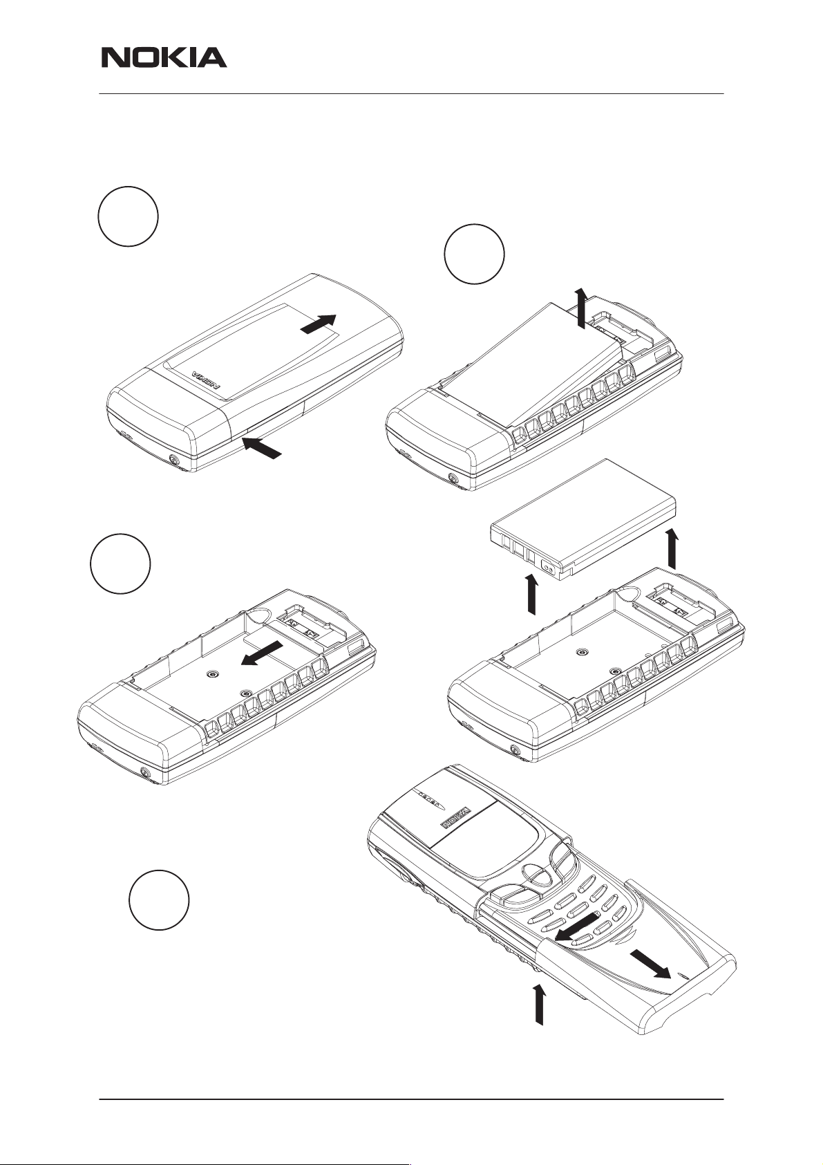
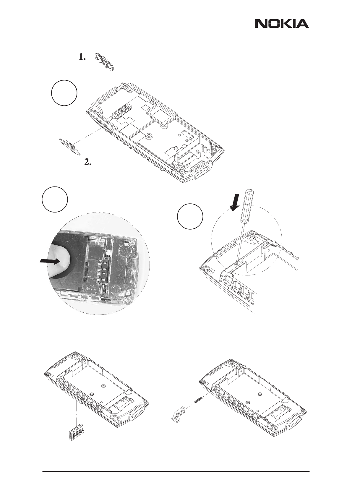
Disassembly of NSM–2
Remove battery.
Step 1. Press the button on the side.
1.
Step 2. Slide the cover downwards and
the cover will be released.
2.
NSM–2
Disassembly & Troubleshooting Instructions
Step 3. Lift the battery first
2.
from the lower end.
Step 4. Remove the battery.
3.
1.
Remove the SIM card from its location.
4.
Step 1. Open the slide cover.
Step 2. Push the slide edge outwards.
NOTE: Use only numbered side 2 to release the slide.
Step 3. Lift the slide up simultaneously and the slide
will be released.
Issue 1 12/1999
Remove the slide cover.
Nokia Mobile Phones Ltd.
3.
2.
1.
Page 3
Page 4
NSM–2
Disassembly & Troubleshooting Instructions
PAMS Technical Documentation
Remove the antenna.
Remove A–cover, speaker
7.
and power button.
5.
Step 1. To remove the antenna, push with the thin spike
of SRT–3 (Battery Connector Extractor Tool) forward to
release the snaps.
Step 2. Release snap fixing using screw driver.
Step 3. Lift up the antenna.
NOTE: Models with no hole in the frame, push firmly the
antenna (1. arrow direction) to release the snaps. Use
screw driver to release snap fixing (2. arrow). Lift up the
antenna (3. arrow).
NOTE: Be careful not brake the middle frame.
6.
Remove the frame
screws (4 pcs).
Screws are numbered according to
the tightening order.
4
3
NOTE: When
assembling the
screws, use 17
Ncm torque.
8.
2
1
Remove keymat module
screws (2 or 3pcs depending on the model).
Page 4
NOTE: When assembling the
screws, use 17 Ncm torque.
Nokia Mobile Phones Ltd.
Issue 1 12/1999
Page 5
PAMS Technical Documentation
Disassembly & Troubleshooting Instructions
Push SW/slide switch before removing
the keymat module. Now remove the
9.
keymat module and rtc–battery.
NOTE: Be careful not to damage the
SW/slide switch on the PCB.
NSM–2
10.
Parts can be separated:
– lcd module
– PCB
– buzzer rubber
– metal gasket
– bottom connector
– SIM connector
– vibra
Issue 1 12/1999
Nokia Mobile Phones Ltd.
Page 5
Page 6
NSM–2
Disassembly & Troubleshooting Instructions
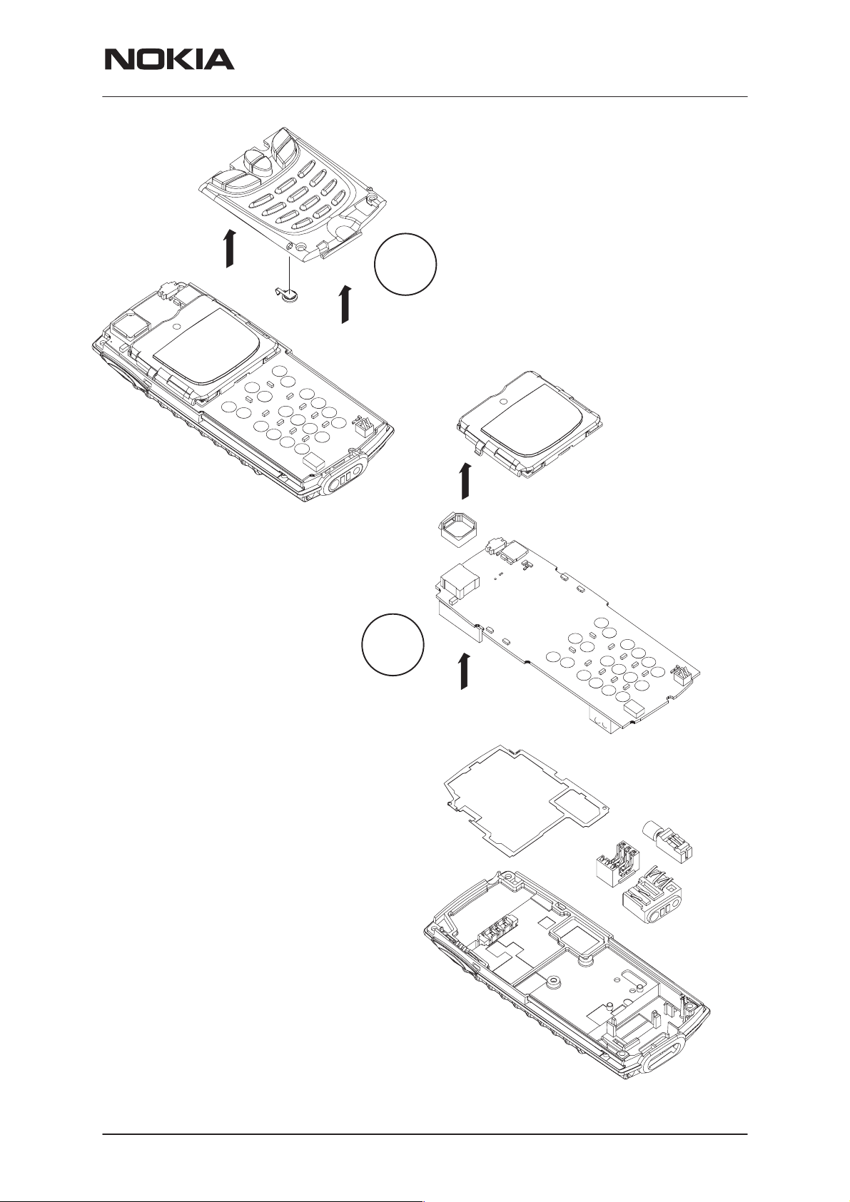
Remove the volume switch 1.
11.
Remove the volume key 2.
PAMS Technical Documentation
12.
Turn the phone around.
Press down battery conector springs
using Battery Connector Extractor Tool.
Battery connector will be released.
13.
Release the latch snap.
Remove the latch and latch spring.
Page 6
Nokia Mobile Phones Ltd.
Issue 1 12/1999
Page 7
PAMS Technical Documentation
Disassembly & Troubleshooting Instructions
Transceiver Troubleshooting
Baseband Troubleshooting
Because of the underfilling of the MAD and combo memory , it is impossible
to change those.
PCB Test Points
Reference Signal Note
C213 RFC MAIN CLOCK (13MHz)
J100* PWM CHARGE CURRENT CONTROL
J101 FBUSTX FBUS TRANSMITTED DA TA
NSM–2
HAGAR (N505) –> MAD (D200)
CCONT (N100) –> CHAPS (N101)
MAD (D200) –> SERVICE INTERFACE
J102 FBUSRX FBUS RECEIVED DA TA
SERVICE INTERFACE –> MAD (D200)
J103 MBUS ONE WIRE TWO DIRECTION SERIAL BUS
(9600 BIT/S)
MAD (D200) <–> SERVICE INTERFACE
J104 CCONT CSX CCONT (N100) CHIP SELECT
MAD (D200) –> CCONT (N100)
J223 CCONT INT CCONT (N100) INTERRUPT
MAD (D200) –> CCONT (N100)
J226 VCXOPWR 26MHz SYSTEM CLOCK CONTROL
MAD (D200) –> VCXO (G830)
J227 PURX POWER UP RESET
CCONT (N100) –> MAD (D200)
J228 SLEEPCLK SLEEP CLOCK (32kHz)
CCONT (N100) –> MAD (D200)
J230 GND GROUND
J234* HAGAR _RESET_X HAGAR (N505) RESET
MAD (D200) –> HAGAR (N505)
J235 ROM1SELX FLASH CHIP SELECT
MAD (D200) –> COMBO MEMORY (D210)
J236 RAMSELX RAM CHIP SELECT
MAD (D200) –> COMBO MEMORY (D210)
Issue 1 12/1999
J237 SYNTHDATA
(SDATA)
J239 DSPXF NOT CONNECTED
J240 MCURDX MCU READ
J241 MCUWRX MCU WRITE
J242 MCUAD1 MCU ADDRESS LINE 1
HAGAR (N505) SERIAL DA TA
MAD (D200) –> HAGAR (N505)
MAD (D200) –> COMBO MEMORY (D210)
MAD (D200) –> COMBO MEMORY (D210)
MAD (D200) –> COMBO MEMORY (D210)
Nokia Mobile Phones Ltd.
Page 7
Page 8

NSM–2
Disassembly & Troubleshooting Instructions
J245* SCLK HAGAR (N505) SERIAL CLOCK
J250 COBBA CSX COBBA (N250) CHIP SELECT
J251 COBBA SDA COBBA (N250) SERIAL BUS DATA
J252 COBBA CLK COBBA (N250) SERIAL BUS CLOCK
J253 PCMRXDAT A AUDIO RECEIVED DA TA
J254 PCMDCLK AUDIO DATA CLOCK (512KHz)
J255 PCMSCLK AUDIO SYNC CLOCK (8kHz)
J255 ESYSRESETX COMPOMEMORY (D210) ENABLE
PAMS Technical Documentation
NoteSignalReference
MAD (D200) –> HAGAR (N505)
MAD (D200) –> COBBA (N250)
MAD (D200) <–> COBBA (N250)
MAD (D200) –> COBBA (N250)
COBBA (N250) –> MAD (D200)
MAD (D200) –> COBBA (N250)
MAD (D200) –> COBBA (N250)
MAD (D200) –> COMBO MEMORY (D210)
J256 PCMTXDATA AUDIO TRANSMITTED DA TA
MAD (D200) –> COBBA (N250)
J257 CCUT (MCUGE-
NIO0)
J258* BUTTON_CTRL
(MCUGENIO1)
J259 MCUGENIO2 NOT CONNECTED
J260 EXTMCUDA0 MCU DATA LINE 0
J299* TXP TRANSMITTER POWER CONTROL
L200 MIC MIC BIAS VOLTAGE, 2.1V IF NO MIC
N310 PIN 13 KBD LIGHT KEYP AD LED LIGHT CURRENT
N310 PIN 14 KBDLED_ADJ KEYPAD BACKLIGHT BRIGHTNESS AD-
N310 PIN 16 VIBRA_CTRL VIBRA DRIVE
CHARGE CUT
MAD (D200) –> CHAPS (N101)
HEADSET BUTTON DETECTION CONTROL
MAD (D200) –> XMICP
MAD (D200) <–> COMPOMEMORY (D210)
MAD (D200) –> RF
V250 –> MIC
UI–SWITCH (N310) –> KEYP AD BACKLIGHT LEDS
JUSTMENT
R311 –> UI–SWITCH (N310)
UI–SWITCH (N310) –> VIBRA (M300)
Page 8
N310 PIN 19 VIBRA VIBRA CONTROL PWM
MAD (D200) –> UI–SWITCH (N310)
N310 PIN 3 BUZZER BUZZER CONTROL PWM
MAD (D200) –> UI–SWITCH (N310)
N310 PIN 6 BUZZER_CTRL BUZZER DRIVE
UI–SWITCH (N310) –> BUZZER (B301)
N310 PIN 7 KBLIGHTS KEYPAD AND DISPLAY BACKLIGHT CON-
TROL
MAD (D200) –> UI–SWITCH (N310)
Nokia Mobile Phones Ltd.
Issue 1 12/1999
Page 9

PAMS Technical Documentation
N310 PIN 8 LCDLED_ADJ LCD BACKLIGHT BRIGHNESS ADJUST-
N310 PIN 9 LCD LIGHT LCD LED LIGHT CURRENT
N400 PIN 4 IRONX IRDA (N400) SHUTDOWN
N401 PIN 4 IRDA POWER 2.8V
R118 PWRONX POWER ON BUTTON
R206 SENA HAGAR (N505) CHIP SELECT
R211 VPP FLASH PROGRAMMING VOLTAGE
R277 EAD ACCESSORY DETECTION
NSM–2
Disassembly & Troubleshooting Instructions
NoteSignalReference
MENT
R310 –> UI–SWITCH (N310)
UI–SWITCH (N310) –> DISPLA Y BACKLIGHT LEDS
MAD (D200) –> IRDA (N400)
N401 –> IRDA (N400)
POWER BUTTON (S330) –> CCONT (N100)
MAD (D200) –> HAGAR (N505)
N220 –> COMPOMEMORY (D210)
XMICP –> CCONT (N100)
Testing
*Only in NSM–2..
The MCU software enters a local mode at start–up if suitable resistors are
connected to the BTEMP and BSI lines.
NOTE! Baseband doesn’t wake up automatically when the battery voltage
is connected. Power must be switched on by
pressing the Power key or
inserting a waking pulse BTEMP line or
connecting a charger
In the local mode the baseband can be controlled through MBUS or
FBUS connections by a PC–locals software. Baseband internal connections are tested with selftests if possible.
Parameters cannot be set accurate enough by design because of component tolerances. Due to use of 5% resistor values, the channels of the
CCONT A/D converters need to be aligned in the production phase. Within battery voltage tuning the MCU software reads the A/D reading from
CCONT at 4.1V and stores this reading to emulated EEPROM memory as
a reference point. Another reference point is created by assuming that
while the input voltage is zero, A/D reading is also zero. Now the slope is
known and A/D readings can be calibrated. Calibration is included in
VBATT A/D reading task.
Issue 1 12/1999
Nokia Mobile Phones Ltd.
Page 9
Page 10

NSM–2
Disassembly & Troubleshooting Instructions
Troubleshooting
Troubleshooting instructions are divided into following sections:
How to check/fix the system/sleep clock.
How to check/fix the power supplies.
Contact service case.
How to check/fix the SIM faults.
How to check/fix the Audio faults.
How to check/fix the charger faults.
The first thing to do is to carry out a thorough visual check of the module.
Make sure that:
– there are no mechanical damages
– solder joints are OK
Before changing anything ALL SUPPLY VOLTAGES AND SYSTEM
CLOCK / SLEEP CLOCK should be checked.
PAMS Technical Documentation
26MHz VCXO
G830
HAGAR
N505
/2
13MHz
Clock signal
buffer
V800++
MAD
C213
Page 10
Nokia Mobile Phones Ltd.
Issue 1 12/1999
Page 11

PAMS Technical Documentation
System Clock
Check the signal from the C213
Layout picture B signal RFC,
should be like in SYSTEM
CLOCK picture.
IF NOT
Check the signal from the RF side
buffer input C829. If there is signal,
check the R829,R834,R830,V800,
C834 and L800
IF THERE ISN’T
NSM–2
Disassembly & Troubleshooting Instructions
Check the signal from the RF side
oskilator VCXO G830 output fron
C833. There should be 26MHz
signal.
IF THERE ISN’T
Change the VCXO
G830
IF IS
Change the Hagar
N505
System clock picture.
Issue 1 12/1999
Nokia Mobile Phones Ltd.
Page 11
Page 12

NSM–2
Disassembly & Troubleshooting Instructions
Sleep Clock
Check the signal from the J228
Layout picture B signal Clk 32kHz,
should be like in SLEEP CLOCK
picture.
IF NOT
Check R100, R154, R102,
C102, C101, C113 and B100
IF OK
Change the CCONT
N100
PAMS Technical Documentation
Page 12
Sleep clock picture.
Nokia Mobile Phones Ltd.
Issue 1 12/1999
Page 13

PAMS Technical Documentation
Power Supplies
Measure power supplies. Test points are shown in layout picture A.
NSM–2
Disassembly & Troubleshooting Instructions
Vbat
Vbb
Vcore
Vsyn2
Vsyn1
VTX
VRX
Vcobba
Vref
VXO
A
Issue 1 12/1999
Nokia Mobile Phones Ltd.
Page 13
Page 14
NSM–2
Disassembly & Troubleshooting Instructions
Vbb = 2.7V – 2.87V
Vcore = 1.3V – 2.65V
Vcobba = 2,67V – 2.85V
Vref = 1.48V – 1.523V
Vbat = 3.11V – 4.2V
VXO = 2,67V – 2.85V
VRX = 2,67V – 2.85V
VTX = 2,67V – 2.85V
Vsyn1 = 2,67V – 2.85V
Vsyn2 = 2,67V – 2.85V
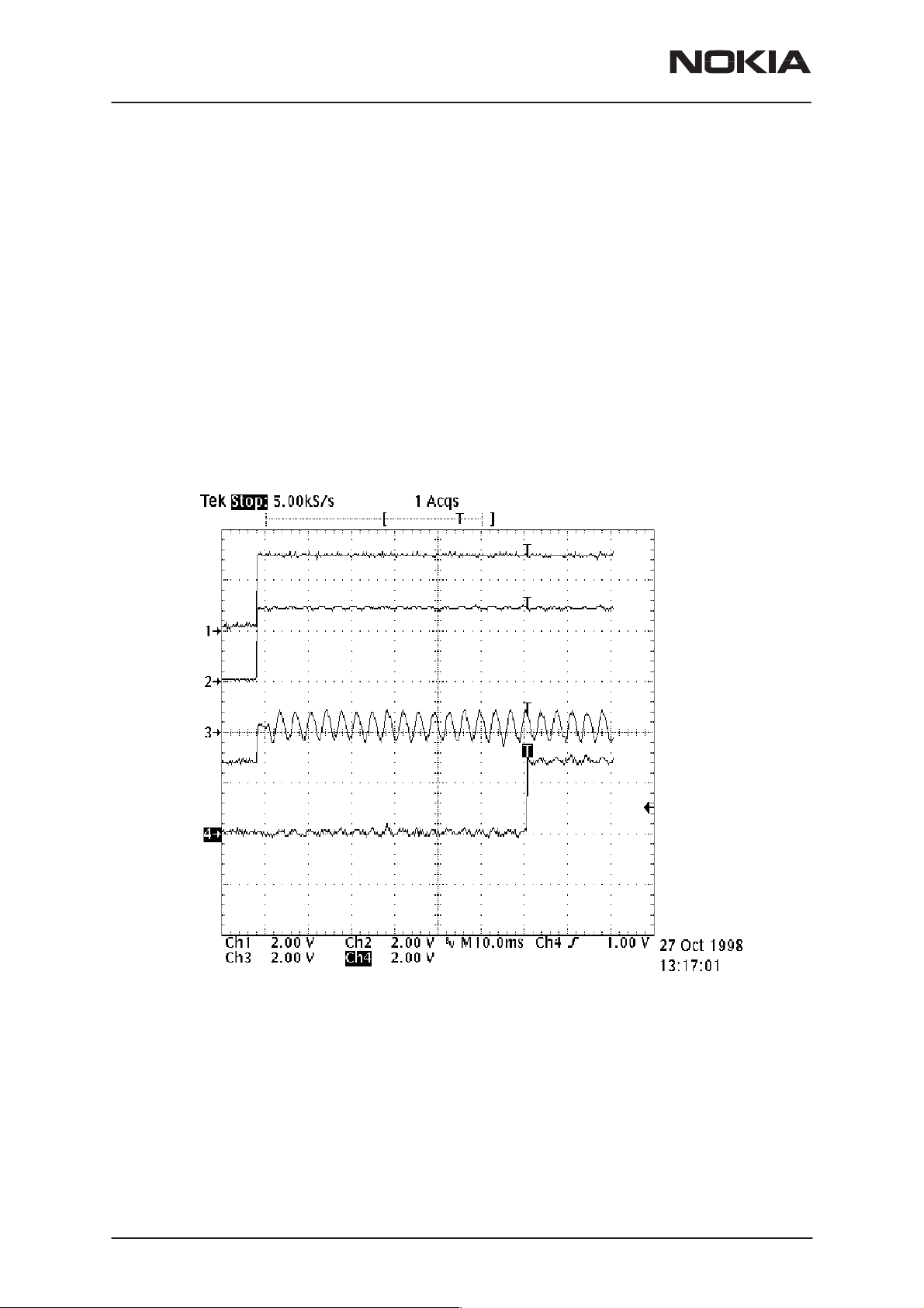
Power up sequence test:
Cconts digital parts keep MAD in reset by keeping PURX down for a
delay of 62ms.
PAMS Technical Documentation
Page 14
Here is shown the start up sequence picture.
Ch1 = Vbb
Ch2 = VXO
Ch3 = SleepClk
Ch4 = PURX (see picture B)
Nokia Mobile Phones Ltd.
Issue 1 12/1999
Page 15

PAMS Technical Documentation
z
X
NSM–2
Disassembly & Troubleshooting Instructions
B
Xf
CLK 32 kH
PURX
Ccont int.
VXO Pwr
ESysReset
RFC
CUAd1
MCUWrX
MBUS
FBUSRx
MCURdX
FBUSTx
ROM1SelX
Issue 1 12/1999
Nokia Mobile Phones Ltd.
Page 15
Page 16

NSM–2
Disassembly & Troubleshooting Instructions
Phone is totally dead
The phone doesn’t take current at all when the power switch is pressed or
when the watchdog disable pin (X001 pin 11) is grounded. Make sure that
the battery voltage you use is within the specification, i.e. 3.11 .. 4.2 V. If
the voltage is lower, hardware of CCONT (N100) prevents power on.
IF battery voltage is inside the specification Change the CCONT.
Flash programming fails
The flash programming can be done via panel connector X001 or via
dedicated PCB pads. In production, the first programming is done via
panel connector. After this, the panel connector is cut away, thus the programming must be done via PCB pads visible through the shield under
the battery. The main difference between these is that FLASH–programming voltage is produced differently. The fault finding diagrams for flash
programming is shown in the start up sequence picture.
In flash programming error cases the flash prommer can give some information about a fault. The fault information messages could be:
PAMS Technical Documentation
– MCU doesn’t boot
– Serial clock line failure
– Serial data line failure
– External RAM fault
– Algorithm file or alias ID not found
– MCU flash Vpp error
Power doesn’t stay on or phone is jammed
If this kind of fault has come after flash programming, there are most
probably open joints in ICs. Solder the joints of ICs. Normally the power
will be switched off by CCONT (N100) after 30 seconds if the watchdog of
the CCONT can not be served by software. This updating can be seen
with an oscilloscope at CCONTCSX (J104). In normal case there is a
short pulse from “1” to “0” every 8 seconds. The power off function can be
prevented by connecting WDDIS (R118 edge side head) to ground.
Because of the underfill, check the supply voltages, clock signals and
power up sequence. If power on sequence fails, there are some open
connections under MAD or compomemory. If all seems to be correct, it is
best way to erase the flash memory and try to put new software to phone.
Contact Service on the phone display
This fault means that software is able to run and thus the watchdog of
CCONT (N100) can be served. Selftest functions are run when power is
switched on and software is executed from flash. If any of the selftests
fails, a “contact service” text is shown on display.
MCU self tests are devided to those executed while power up (start up
tests) and ones that can be executed with connected PC. The tests and
included items are as follows:
Page 16
Nokia Mobile Phones Ltd.
Issue 1 12/1999
Page 17

PAMS Technical Documentation
1. MCU ROM checksum
Calculates 16 bit checksum out of Flash code and compares it to one
found in Flash.
Items being checked are:
MAD2 <––> Flash data and address lines, CE0,CE1, WE, BYTE, Vcc,
GND, Flash internal functionality
2. MCU RAM interface
3. MCU RAM component
4. MCU EEPROM interface
5. MCU EEPROM component
6. RTC battery
7. CCONT interface
8. A/D converter
9. SW reset
A. Power off
B. Security data
C. EEPROM tune checksum
D. PPM checksum
E MCU download DSP
F. DSP alive
G. COBBA serial
H COBBA parallel
I. EEPROM checksum
K. PPM validity
NSM–2
Disassembly & Troubleshooting Instructions
Issue 1 12/1999
Nokia Mobile Phones Ltd.
Page 17
Page 18

NSM–2
Disassembly & Troubleshooting Instructions
SIM related faults
The hardware of the SIM interface from MAD2 (D200) to the SIM connector (X302) can be tested without a SIM card. When the power is
switched on and the BSI line is grounded by a resistor, all the used lines
(VSIM, RST, CLK, DATA) rise up to 5 V four times. Thus “Insert SIM card”
faults can be found without SIM card.
The fault information “Card rejected” indicates that ATR message (the first
message is always sent from card to the phone) is sent from card but the
message is somehow corrupted, data signal levels are wrong etc. or factory set values (stored to the emulated EEPROM) are not correct.
PAMS Technical Documentation
Check the Vsim. Is it 3V or 5V
Vsim (C128 bottom connector side
head )
IF NOT OK
Check the Vsrm (C131 RF side head)
V5V (C108 bottom connector side
head)
IF NOT OK
Check the regulator N600, V116, C132
and C131
OK
Check the V104. R128, R125, R124
and C128
OK
Change the CCONT N100
OK
Page 18
Nokia Mobile Phones Ltd.
Issue 1 12/1999
Page 19

PAMS Technical Documentation
Audio faults
earpiece doesn’t work
and there isn’t any
mechanical problem
Check R 292, R291, L272 and L271
OK
Change the COBBA N250
NSM–2
Disassembly & Troubleshooting Instructions
Microphone doesn’t work
and there isn’t any
mechanical problem
Check the voltage in resistor
R267 RF side head. Voltage should be
about 2.1V
OK
Check the R268,C 274,C263,C278
and C262
Check R266, C268, L287 and V250
OK
Change the COBBA N250
Issue 1 12/1999
Nokia Mobile Phones Ltd.
Page 19
Page 20

NSM–2
Disassembly & Troubleshooting Instructions
Headset earpiece doesn’t
work and there isn’t any
mechanical problem
Check R 257,R256, R270, L284, L283
C284, C283, C 296, C 297, C261and C255
OK
Change the COBBA N250
PAMS Technical Documentation
Headset earphone doesn’t
work and there isn’t any
mechanical problem
Check R 257,R256, R270, L284, L283
C284, C283, C 296, C 297, C261and C255
OK
Change the COBBA N250
Page 20
Nokia Mobile Phones Ltd.
Issue 1 12/1999
Page 21

PAMS Technical Documentation
Charging fault
Display ” not charging”
NSM–2
Disassembly & Troubleshooting Instructions
Check charge voltage with wintesla
OK
Check charge current with wintesla
IF NOT OK
Check V101 and R131
OK
Check F101, V100,R104 and
R103
Change the Chaps N101
Issue 1 12/1999
Nokia Mobile Phones Ltd.
Page 21
Page 22

NSM–2
Disassembly & Troubleshooting Instructions
RF Troubleshooting
PA_PCN_out
PA_in
PAMS Technical Documentation
ant_sw_IN
PA_GSM_out
PA_ctrl (GSM)
PA_ctrl (PCN)
PA_buff_in
TXI
TX_balout(PCN)
TXC
TX_balout(GSM)
Vchp
5V5
1.35V (RX)
VCO_out
1.2V (RX)
ant_sw_ctrl (PCN)
ant_sw_ctrl (GSM)
RX_GSM (lna_in)
RX_PCN (lna_in)
RX_PCN (balun_in)
TCXO/2 (13 MHz)
RX_GSM (balun_in)
AFC
RXI (filt)
VCO_ctrl
Page 22
Vtcxo
+1.5V
Vcobba
Vrxrf
Vmod
Nokia Mobile Phones Ltd.
Vsynte
Vlna
TCXO (26 MHz)
RXQ (filt)
TXQ
RX I/Q (ADC)
Issue 1 12/1999
 Loading...