

Page 1

PAMS Technical Documentation
NSE–6 Series Transceivers
Disassembly &
Troubleshooting
Instructions
Original 08/98
Page 2

NSE–6
PAMS
Disassembly & Troubleshooting Instructions
Technical Documentation
CONTENTS
Disassembly 3. . . . . . . . . . . . . . . . . . . . . . . . . . . . . . . . . . . . . . . . .
Baseband Testing 5. . . . . . . . . . . . . . . . . . . . . . . . . . . . . . . . . . . . . . .
Alignments 5. . . . . . . . . . . . . . . . . . . . . . . . . . . . . . . . . . . . . . . . . .
Trouble Shooting 6. . . . . . . . . . . . . . . . . . . . . . . . . . . . . . . . . . . . . . .
Phone is totally dead 7. . . . . . . . . . . . . . . . . . . . . . . . . . . . . . . . . .
Flash programming doesn’t work 7. . . . . . . . . . . . . . . . . . . . . . .
Flash Programming failure (1) 9. . . . . . . . . . . . . . . . . . . . . . .
Flash Programming failure (2) 10. . . . . . . . . . . . . . . . . . . . . . .
Flash Programming failure (3) 11. . . . . . . . . . . . . . . . . . . . . . .
Flash Programming failure (4) 12. . . . . . . . . . . . . . . . . . . . . . .
Power doesn’t stay on, or phone is jammed 13. . . . . . . . . . . . . .
Display Information: Contact Service 14. . . . . . . . . . . . . . . . . . . .
The phone doesn’t register to the network or phone doesn’t make a call 15.
Phone register failure 17. . . . . . . . . . . . . . . . . . . . . . . . . . . . . . .
SIM card related failures 18. . . . . . . . . . . . . . . . . . . . . . . . . . . . . . .
SIM Card failure 19. . . . . . . . . . . . . . . . . . . . . . . . . . . . . . . . . . .
Audio failure 20. . . . . . . . . . . . . . . . . . . . . . . . . . . . . . . . . . . . . . .
Charger failure 21. . . . . . . . . . . . . . . . . . . . . . . . . . . . . . . . . . . . .
Receiver Fault (1) 22. . . . . . . . . . . . . . . . . . . . . . . . . . . . . . . . . .
Receiver Fault (2) 23. . . . . . . . . . . . . . . . . . . . . . . . . . . . . . . . . .
Receiver Fault (3) 24. . . . . . . . . . . . . . . . . . . . . . . . . . . . . . . . . .
Receiver Fault (4) 25. . . . . . . . . . . . . . . . . . . . . . . . . . . . . . . . . .
Receiver Fault (5) 26. . . . . . . . . . . . . . . . . . . . . . . . . . . . . . . . . .
Receiver Fault (6) 27. . . . . . . . . . . . . . . . . . . . . . . . . . . . . . . . . .
Transmitter Fault (1) 28. . . . . . . . . . . . . . . . . . . . . . . . . . . . . . . .
Transmitter Fault (2) 29. . . . . . . . . . . . . . . . . . . . . . . . . . . . . . . .
Transmitter Fault (3) 30. . . . . . . . . . . . . . . . . . . . . . . . . . . . . . . .
Appendix A 31. . . . . . . . . . . . . . . . . . . . . . . . . . . . . . . . . . . . . . . .
Appendix B 32. . . . . . . . . . . . . . . . . . . . . . . . . . . . . . . . . . . . . . . .
Appendix C 33. . . . . . . . . . . . . . . . . . . . . . . . . . . . . . . . . . . . . . . .
Appendix D 34. . . . . . . . . . . . . . . . . . . . . . . . . . . . . . . . . . . . . . . .
Test points 35. . . . . . . . . . . . . . . . . . . . . . . . . . . . . . . . . . . . . . . . . . .
Page No
Page 2
Original 08/98
Page 3
PAMS
NSE–6
Technical Documentation
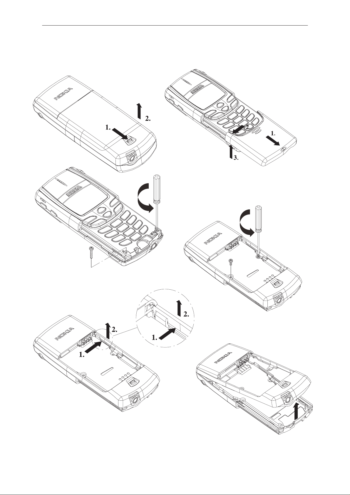
Disassembly
Remove battery
Disassembly & Troubleshooting Instructions
Step 1. Open slide cover.
Step 2. Push slide edge outwards.
Step 3. Lift slide up from the edge
and slide will be released.
Remove a–cover
screws (2 pcs)
NOTE: When assembling the
screws, use 17 Ncm torque.
Turn the phone around and remove C–cover screws (2 pcs)
Step 1. Push c–cover edge outwards to release it behind locking snap
Step 2. Lift up the edge to release c–cover.
Step 3. Repeat the operation on both sides.
Original 08/98
Remove c–cover by
lifting up rear and
pulling cover out.
Page 3
Page 4
NSE–6
PAMS
Disassembly & Troubleshooting Instructions
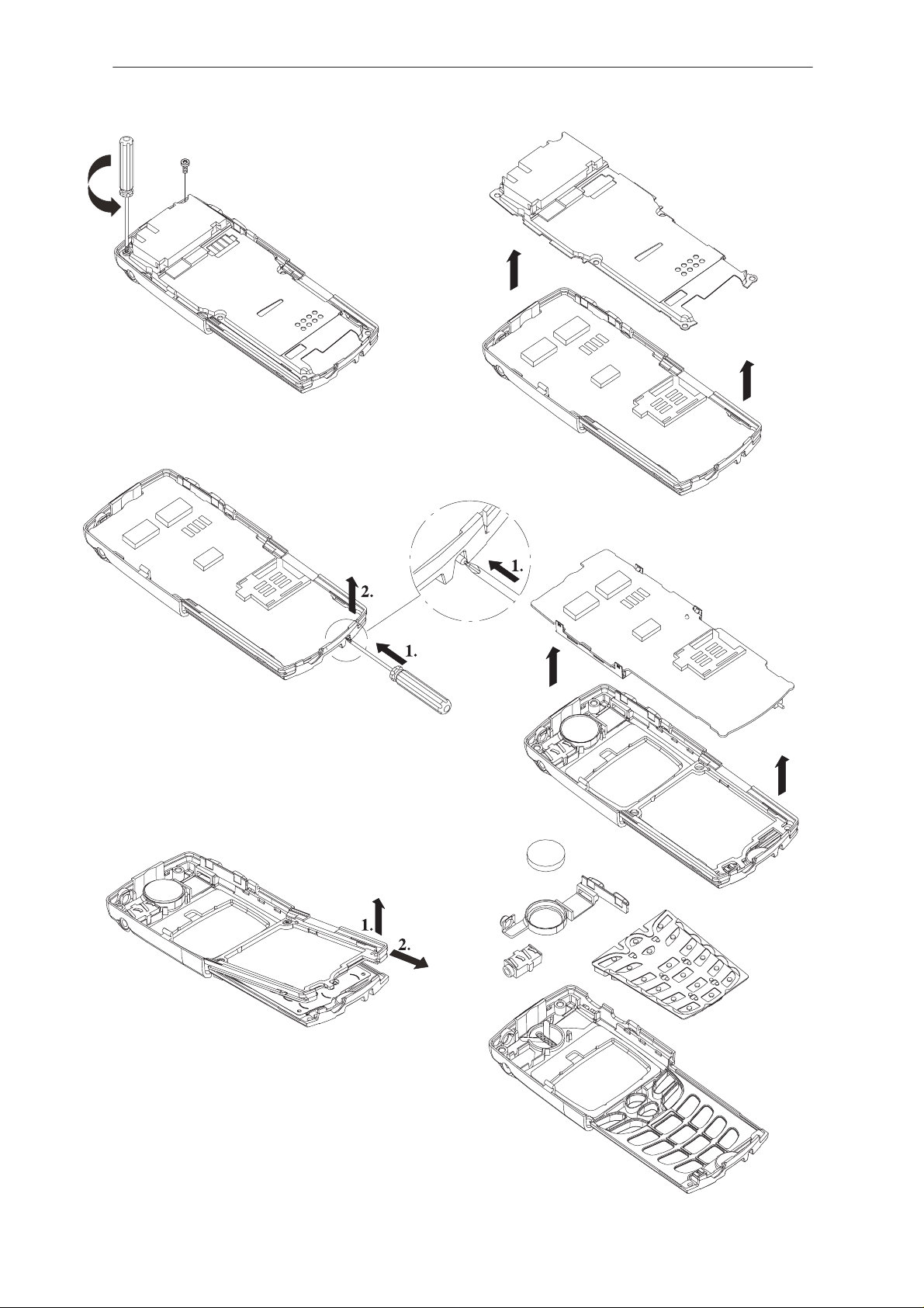
Remove shield
screws (2 pcs).
Step 1. Push slide detector
switch to the bottom and hold.
Step 2. Release main pcb by
lifting rear up and pulling.
Technical Documentation
Remove shield.
Step 1. Lift slide frame from botttom and loosen it from a–cover.
Step 2. Remove slide frame, UI–
board will follow.
Remove main pcb.
Page 4
Parts can be separated.
Original 08/98
Page 5

PAMS
NSE–6
Technical Documentation
Baseband Testing
The MCU software enters a local mode at start–up if suitable resistors are
connected to the BTEMP and BSI lines. NOTE! Baseband doesn’t wake up
automatically when the battery voltage is connected. Power must be
switched on via:
1. Pwr key or
2. BTEMP line or
3. Charger
In the local mode the baseband can be controlled through MBUS or FBUS
connections by a PC–locals software. Baseband internal connections are
tested with self tests if possible. By connecting MAD2 pin ROW5 to ground,
MAD2 pins are toggled as a daisy chain, which can be used for detecting
short circuits in MAD2 pins. Test pads are placed on engine pcb for service
and production troubleshooting purposes in some supply voltage and signal
lines.
Disassembly & Troubleshooting Instructions
Alignments
Within alignment those parameters are adjusted, that cannot be set accurate
enough by design because of component tolerances. Due to use of 5% resistor values, the channels of the CCONT A/D converters need to be aligned
in the production phase. Within battery voltage tuning the MCU software
reads the A/D reading from CCONT at 4.1V and stores this reading to EEPROM memory as a reference point. Another reference point is created by
assuming that while the input voltage is zero, A/D reading is also zero. Now
the slope is known and A/D readings can be calibrated. Calibration is included in VBAT A/D reading task.
Battery charging voltage VCHAR and current ICHAR are calibrated using
one test setting. T est jig in production/service must have a connection to battery terminals. ICHAR and VCHAR are supplied fron the jig and service software calculates values, which are then stored to EEPROM.
Original 08/98
Page 5
Page 6

NSE–6
PAMS
Disassembly & Troubleshooting Instructions
Trouble Shooting
The following hints should facility finding the cause of the problem when
the circuitry seems to be faulty. This trouble shooting instruction is divided following section.
1. Phone is totally dead
2. Flash programming doesn‘t work
3. Power doesn‘t stay on or the phone is jammed
4. Display information: Contact Service
5. Phone doesn‘t register to the network or phone doesn‘t make a call.
6. SIM card related failures ( insert SIM card or card rejected).
7. Audio fault.
8. Charging fault
The first thing to do is carry out a thorough visual check of the module.
Ensure in particular that:
a) there are not any mechanical damages
b) soldered joints are OK
Technical Documentation
Page 6
Original 08/98
Page 7
PAMS
NSE–6
Technical Documentation
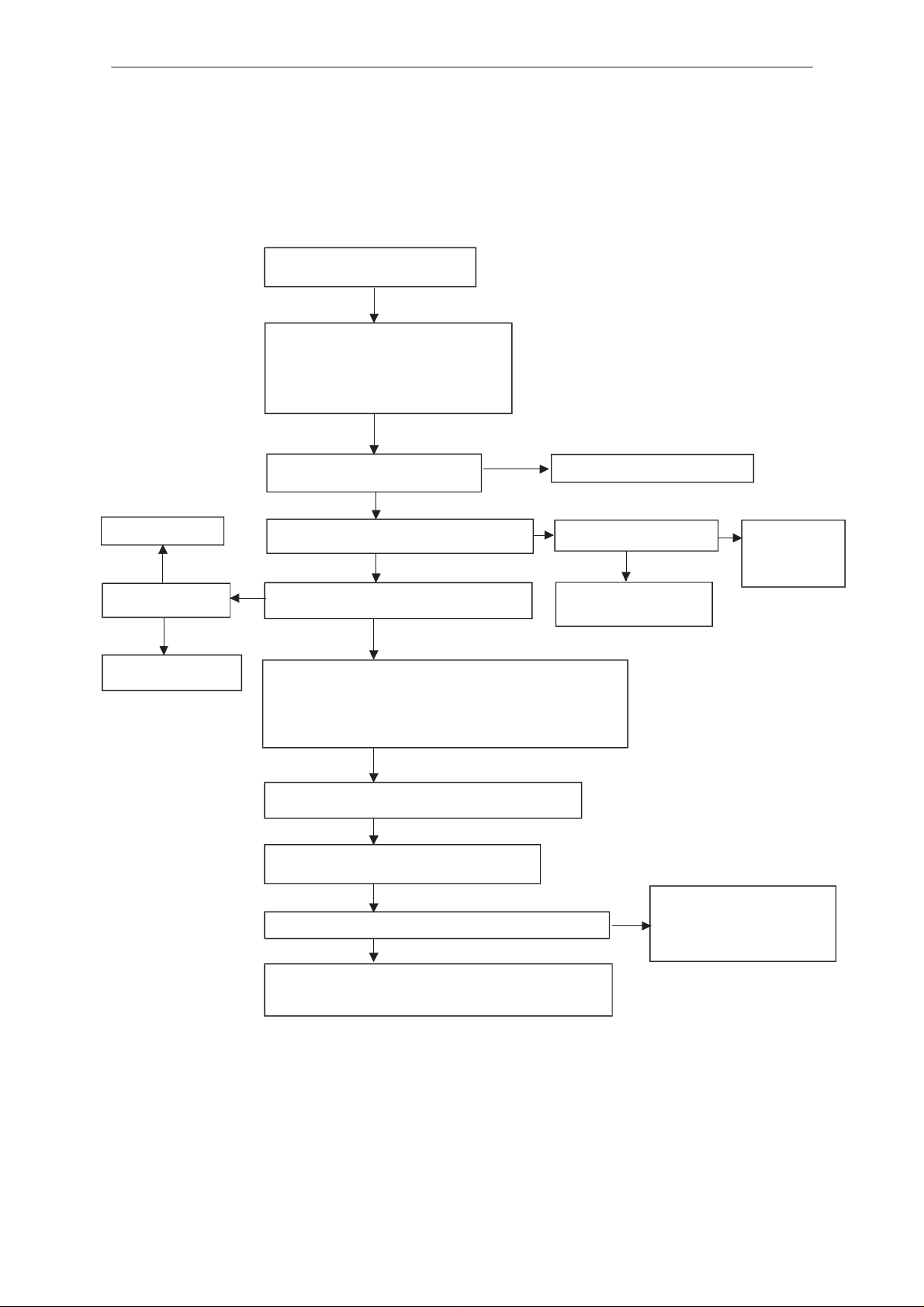
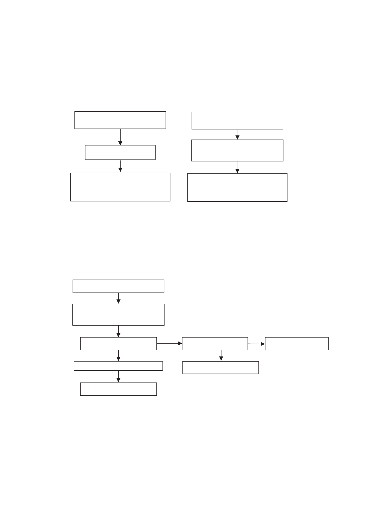
Phone is totally dead
This means that the phone doesn’t take current at all when the power
switch is pressed or when the watchdog disable pin (X001 pin 11, J111) is
grounded. Used battery voltage must be higher than 3.1 V. Otherwise the
hardware of CCONT (N100) prevents totally power switch–on.
Phone is totally dead
Yes
J232 VBAT is 3.6 V
Yes
Voltage at J111 is 3.6V
Disassembly & Troubleshooting Instructions
No
Failure in VBA T line
Check L103
No
Faulty CCONT (N100)
Yes
VBB 2.8 V (R115, C107..)
VXO 2.8 V (C149..)
When PWR switch is pressed or
WDDIS is grounded (J111)
Yes
See section ”Power doesn’t stay on”
No
WDDIS (J111)) is
0V, when PWR switch
is pressed
Faulty CCONT (N100)
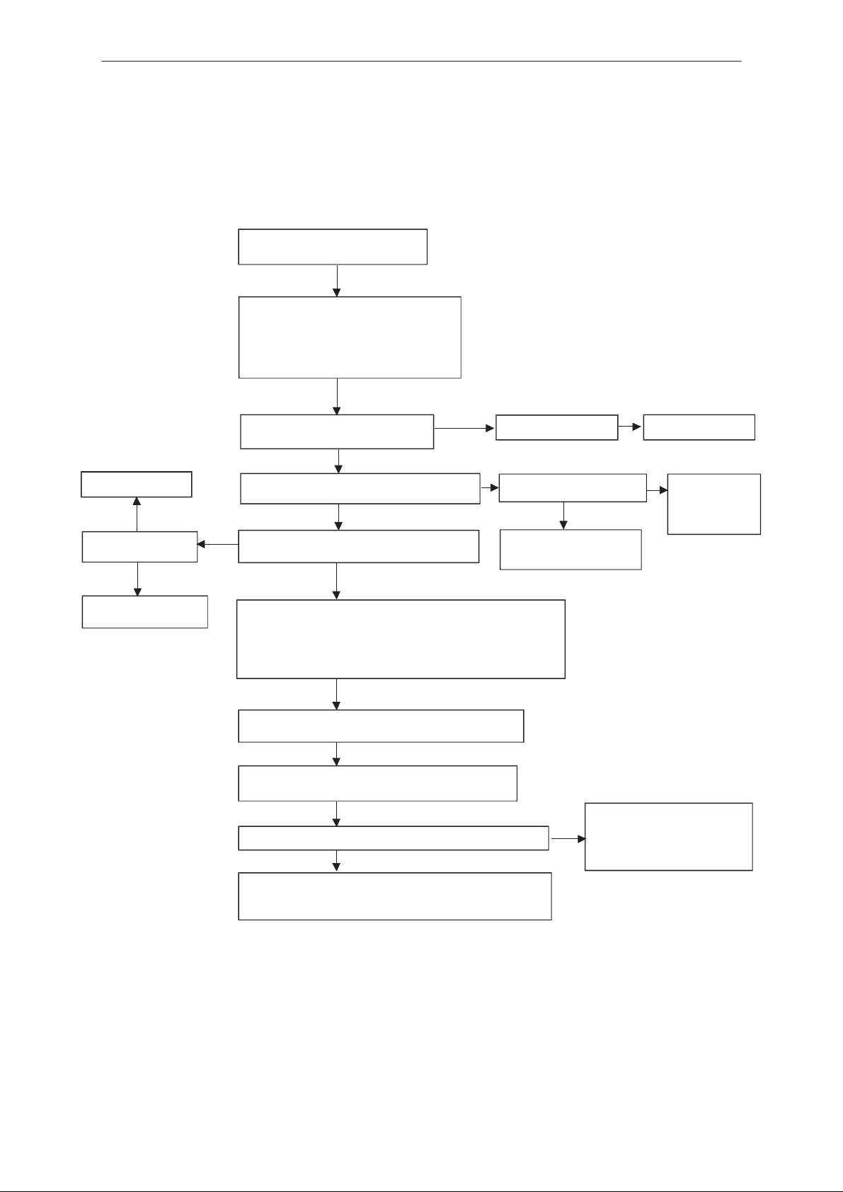
Flash programming doesn’t work
The flash programming can be done via panel connector X001 or via dedicated PCB pads. In production, the first programming is done via panel
connector. After this, the panel connector is cut away, thus the programming must be done via PCB pads visible through the shield under the battery. The main difference between these is that FLASH programming voltage is produced differently.
Yes
No
Check PWR switch
to CCONT line: R341,
R1 18
In flash programming error cases the flash prommer can give some information about a fault. The fault information messages could be:
– MCU doesn’t boot
– Serial clock line failure
– Serial data line failure
– External RAM fault
– Algorithm file or alias ID don’t find
– MCU flash Vpp error
Original 08/98
Page 7
Page 8
NSE–6
PAMS
Disassembly & Troubleshooting Instructions
In cases of unsuccesful flash programming there is a possibility to check
short circuits between the memories and the MCU (MAD2). It is useful to
do this test, when the fault information is: MCU doesn’t boot, Serial clock
line failure or Serial data line failure. The test procedure is following:
1. Connect testpoint J229 to ground.
2. Switch the power on.
3. If the voltage level in testpoint J225 is 2.8 V (”1”), the interface is OK. If
there is a short circuit, the voltage level in testpoint J225 stays low and 32kHz
square wave signal can be seen in the lines which are already tested.
It must be remembered that this test can only find short circuits, not open
pins. In addition upper data lines (15:8) of flash memory D220 are not included in this test.
CCONT pin 54
Technical Documentation
( PURX )
passed
MAD pin 38
MAD pin 134
J225
( MCUAD0)
( ExtSysResX))selftest
Page 8
Original 08/98
Page 9
PAMS
NSE–6
Technical Documentation
Flash Programming failure (1)
Flash programming doesn’t work
via panel connector
YES
If the fault information from prommer is:
a) MCU doesn’t boot
b) Serial data line failure
c) Serial clock line failure
connect watchdog disable (WDDIS, J111)
line to the ground
OK
VBB (R115, C107 upper side) 2.8 V
VXO (C149 upper side ) 2.8 V
YES
Check C213, R213
YES
NO
RFC (C664) 13 MHz
800 mV min
NO
J227 master reset (Purx) = ”1” (2.8 V)
YES
RfClk (R213 lower side) 13 MHz sine wave
clock signal: 500 mV
pp
YES
Disassembly & Troubleshooting Instructions
NO
See section ”Phone is totally dead”
NO
J228 sleep clock (SCLK)
square wave 32 kHz
YES
min
Faulty circuit N100
or overloaded PurX line
NO
Check sleep
clock circuitry
(B101, R154..)
Check buffer V660 and
VCTCXO G660
Check that following lines are correct:
FTX (fbus_tx) line: X001 pin 1 ––> R215
FRX (fbus_rx) line: X001 pin 2 ––> R201
FCLK (MBUS) line: X001 pin 3 ––> R115
Check also pullup and pulldown resistors R115, R201, R215
GND: X001 pin 7 ––> GND
OK
Enable the selftest function of D200 by connecting
J229 to ground
Connect oscilloscope to testpoint J225
(ExtSysResetX) and switch power on
Voltage level rises to ”1” after power on at testpoint J225
YES
There could be open pins in circuits D200 (D220, D240)
(open joints may be detectable with microscope)
If not, the PCB or D200 (D220, D240) is faulty.
There is a shortcircuit
NO
somewhere in memory control
lines or MCU address lines or
MCU lower (7:0) data lines
Original 08/98
Page 9
Page 10
NSE–6
PAMS
Disassembly & Troubleshooting Instructions
Flash Programming failure (2)
Flash programming doesn’t work
via panel connector
If the fault information is:
External RAM fault
Check control lines of SRAM (D230):
RamSelX (J235)..
There could be open joints in SRAM
Technical Documentation
Flash programming doesn’t work
via panel connector
If the fault information is:
Algorithm file or alias ID don’t find,
ID is unknown etc.
Check control lines of Flash (D220):
ROM1SelX (J234)..
Fault could be open joints in Flash or
In upper data lines (15:8)
Flash programming doesn’t work
via panel connector
If the fault information is:
MCU flash Vpp error
Check connections between X001;10
––> R21 1 upper side
Check components C212, R211
Faulty component D220
Page 10
Original 08/98
Page 11
PAMS
NSE–6
Technical Documentation
Flash Programming failure (3)
Flash programming doesn’t work
If the fault information from prommer is:
a) MCU doesn’t boot
b) Serial data line failure
c) Serial clock line failure
connect watchdog disable (WDDIS, J111)
line to the ground
VBB (R115, C107 upper side) 2.8 V
VXO (C149 upper side ) 2.8 V
Check C213, R213
YES
RFC (C664) 13 MHz
800 mV min
NO
NO
J227 master reset (Purx) = ”1” (2.8 V)
RfClk (R213 lower side) 13 MHz sine wave
clock signal: 500 mV
YES
OK
YES
YES
pp
YES
min
Disassembly & Troubleshooting Instructions
NO
VBAT is correct 3.6 V
NO
J228 sleep clock (SCLK)
square wave 32 kHz
YES
Faulty circuit N100
or overloaded PurX line
YES
Faulty circuit N100
NO
Check sleep
clock circuitry
(B101, R154..)
Check buffer V660 and
VCTCXO G660
Check that following lines are correct:
FTX (fbus_tx) line: X001 pin 1 ––> R215
FRX (fbus_rx) line: X001 pin 2 ––> R201
FCLK (MBUS) line: X001 pin 3 ––> R115
Check also pullup and pulldown resistors R115, R201, R215
GND: X001 pin 7 ––> GND
OK
Enable the selftest function of D200 by connecting
testpoint J229 to ground
Connect oscilloscope to testpoint J225
(ExtSysResetX) and switch power on
Voltage level rises to ”1” after power on at testpoint J225
YES
There could be open pins in circuits D200 (D220, D240)
(open joints may be detectable with microscope)
If not, the PCB or D200 (D220, D240) is faulty.
There is a shortcircuit
NO
somewhere in memory control
lines or MCU address lines or
MCU lower (7:0) data lines
Original 08/98
Page 11
Page 12
NSE–6
PAMS
Disassembly & Troubleshooting Instructions
Flash Programming failure (4)
Flash programming doesn’t work
If the fault information is:
External RAM fault
Check control lines of SRAM (D230):
RamSelX..
There could be open joints in SRAM
Technical Documentation
Flash programming doesn’t work
If the fault information is:
Algorithm file or alias ID not found,
ID is unknown etc.
Check control lines of Flash (D220):
ROM1SelX (J234)..
Fault could be open joints in Flash or
In upper data lines (15:8)
Flash programming doesn’t work
YES
If the fault information is:
MCU flash Vpp error
YES
Vpp > 2.8 V (C212)
YES
Check components C212, R211
OK
Faulty component D220
NO
Vpp > 2.8 V in J221
YES
Check UI connector X303
NO
Check regulator N202
Page 12
Original 08/98
Page 13

PAMS
NSE–6
Technical Documentation
Disassembly & Troubleshooting Instructions
Power doesn’t stay on, or phone is jammed
If this kind of fault has come after flash programming, there are most
probably open joints in ICs. The solder joints of ICs: MAD2 (D200), Flash
(D220) and SRAM (D230) are to be checked at the extent possible (by
microscope from the side of PCB and lightly pressing components while
switching power on).
Normally the power will be switched off by CCONT (N100) after 30 seconds if the watchdog of the CCONT can not be served by software. This
updating can be seen with an oscilloscope at CCONTCSX (J236). In normal case there is a short pulse from “1” to “0” every 8 seconds. The power off function can be prevented by connecting WDDIS (J111) to ground.
Check C213, R213
YES
RFC (C664) 13 MHz
800 mV min
NO
Check buffer V660
and VCTCXO G660
Power doesn’t stay on or phone is jammed
YES
CCONT watchdog is served?
(J236 pulses 1 ––> 0 every 8 sec)
NO
Connect J111 (WDDIS) to GND
OK
VBB (C107 upper side) 2.8 V
VXO (C149 upper side) 2.8 V
YES
Master reset PURX (J227) 2.8 V
NO
RfClk (R213 lower side) 13 MHz sine wave
clock signal: 500 mVpp min
Open pins or faulty circuit:
D200, D220, D230, N100, R215
Flashing can give information in deciding
which IC to change. Changed Flash ID
for example indicates Flash failure
YES
YES
YES
NO YES
Software is able to run
If power is switched off after
few seconds, check BSI and
BTEMP lines
VBAT is 3.6 V
NO NO
Sleep clock SCLK (J228)
square wave 32 kHz
YES
N100 faulty or
overloaded PurX line
N100 faulty
Check sleep clock
circuitry (B101, R154..)
Original 08/98
Page 13
Page 14

NSE–6
PAMS
Disassembly & Troubleshooting Instructions
Display Information: Contact Service
This fault means that software is able to run and thus the watchdog of
CCONT (N100) can be served. Selftest functions are run when power is
switched on and software is executed from flash. If any of the selftests
fails, a “contact service” text is shown on display.
MCU self tests are devided to those executed while power up (start up
tests) and ones that can be executed with connected PC. The tests and
included items are as follows:
1. MCU ROM checksum
Calculates 16 bit checksum out of Flash code and compares it to one
found in Flash. Items being checked are:
MAD2 <––> Flash data– and address lines, CE0,CE1, WE, BYTE, Vcc,
GND, Flash internal functionality
2. MCU RAM interface
3. MCU RAM component
4. MCU EEPROM interface
5. MCU EEPROM component
6. RTC battery
7. CCONT interface
8. A/D converter
9. SW reset
A Power off
B. Security data
C. EEPROM tune checksum
D. PPM checksum
E MCU download DSP
F. DSP alive
G. COBBA serial
H COBBA parallel
I. EEPROM sec checksum
K. PPM validity
Technical Documentation
Page 14
Original 08/98
Page 15

PAMS
NSE–6
Technical Documentation
Disassembly & Troubleshooting Instructions
The phone doesn’t register to the network or phone
doesn’t make a call
If the phone doesn’t register to the network or the phone doesn’t make a
call, the reason could be either on baseband or RF. The phone can be set
to wanted mode with WinTesla service software in order to find out whether the fault is in RF or in baseband (RF interface measurements).
The control lines for RF are supplied both by the System Asic (inside of
MAD2;D200) and the RFI (inside of Cobba; N250). MAD2 handles digital
control lines (like SENA, TxP etc.) and Cobba handles analog control
lines (like AFC, TxC etc.). The DSP software is constructed so that operation states of DSP (MAD2) can be seen in external flag, DSPXF (J222).
After power up, DSP will signal all the completed functions by changing
the state of the XF pin.
1. DSP initialization done
2. Synchronization to network done
3. Registration to network done
321
DSPXF (J222)
Original 08/98
Page 15
Page 16

NSE–6
PAMS
Disassembly & Troubleshooting Instructions
init inialize
Patch code
download
Technical Documentation
1
DSP
constants
download
Iinitialization
done
2
channel
scan
starts
search
Send RACH
RACH OK
(transmitter on)
Last PSW OKPSW
Sycronization
OK
3
Go SDCCH immediate
assignment OK
(phone in serve state)
Page 16
Original 08/98
Page 17

PAMS
NSE–6
Technical Documentation
Phone register failure
Phone doesn’t register to network or
phone doesn’t make a call
Analog supply voltage VCOBBA is > 2.7
at C280 (C281, C282..)
Analog reference voltage Vref is 1.5
at C251 (R253 lower side)
– During the receiving slot:
Supply voltage VCP (J220) > 4.8
Supply voltage VRX (C148, C543..) > 2.7
Supply voltage VSYN_1 (C144, C505..) > 2.7
Supply voltage VSYN_2 (C143, C641..) > 2.7
– During the transmitting slot:
Supply voltage VTX (C145, C746..) > 2.7
YES
YES
YES
Disassembly & Troubleshooting Instructions
NO
V
NO
V
V
V
V
V
V
Check CCONT (N100)
Check R253, R251
NO
Check CCONT, MAD2
(N100, D200)
YES
Synthesizer lines:
SEna: Summa N540 pin 7
SClk: Summa N540 pin 5
SData: Summa N540 pin 6
pulses 0 ––> 1 during receiving slot
YES
RF control lines:
RxC (R263 upper side) 0 ––> 2.3 Vmax
AFC (R660 upper side) 0 –– 1.2
during receiving slot
YES
Analog data signals RxIP and RxIN (R544 upper sides)
0 ––> 1.5 V DC during receiving slot
Used benefit signal is biased to DC and its amplitude
is 50 mVpp nominal and frequency is 13 MHz
YES
RF control lines:
TxC (R740 upper side) 0 ––> 2.3 Vmax
TxP (Summa N540 pin 32) 0 –– 2.8 V
during transmitting slot
YES
Analog data signals TxIN, TxIP, TxQN, TxQP
(R749, R748, R746, R745 upper sides respectively)
0 ––> 0.8 V DC during transmitting slot
Used benefit signal is biased to DC and its amplitude
is 300 mVpp nominal and frequency is 64 kHz
Vtyp
NO
Check MAD2 (D200)
NO
Check COBBA (N250)
NO
Check COBBA (N250) if DC failed
Check RF if benefit signal failed
NO
Check COBBA (N250) if TxC failed
Check RF if benefit signal failed
NO
Check COBBA (N250)
YES
Check RF
Original 08/98
Page 17
Page 18

NSE–6
PAMS
Disassembly & Troubleshooting Instructions
SIM card related failures
The hardware of the SIM interface from MAD2 (D200) to the SIM connector (X451) can be tested without a SIM card. When the power is switched
on and the BSI line (J122) is grounded by a resistor, all the used lines
(VSIM, RST, CLK, DATA) rise up to 5 V four times. Thus “Insert SIM card”
faults can be found without SIM card.
The fault information “Card rejected” indicates that ATR message (the first
message is always sent from card to the phone) is sent from card but the
message is somehow corrupted, data signal levels are wrong etc. or factory set values (stored to the EEPROM) are not correct.
Insert SIM card failure
YES
Voltage < 1.5 V at C120 when
BSI resistor is connected
Technical Documentation
NO
Check R120. R122, C120,
Battery connector
YES
VSIM, DATA, RESET and CLOCK lines
(J252, J116, J118, J117) rise up to 5V
after power on
NO
VSIM, DATA_O,SIMRST_O and SIMCLK_O lines
rise up to 5V after power on at pins of SIM card
NO
SIMPWR, SIMRST_A, SIMCLK, SIMIO_C
lines (J1 12, J113, J114, J115) rise up to 2.8 V
after power on
NO
MAD2 (D200) or PCB is faulty
YES
Check SIM card and SIM
reader connectors
YES
Check
R124, R125, R128, X451
YES
Faulty circuit
N100 (CCONT)
Page 18
Original 08/98
Page 19

PAMS
NSE–6
Technical Documentation
SIM Card failure
Card rejected fault
VSIM (J252):
2.8 V min (with 3 V SIM card)
4.5 V min (with 5 V SIM card)
The ATR data can be seen at J116
SIMIOControl line (J1 15) is ”1”
during the ATR message
YES
YES
YES
YES
Disassembly & Troubleshooting Instructions
NO
CCONT (N100) faulty
NO
Check R124, X451
NO
Check MAD2 (D200)
Check MAD2 (D200)
Original 08/98
Page 19
Page 20

NSE–6
PAMS
Disassembly & Troubleshooting Instructions
Audio failure
Uplink (microphone) and downlink
(earphone) are disfunctional
YES
NO
Voltage at HOOKDET (C260)
2.8 V (without headset)
YES
NO
Voltage at HEADDET (C261)
2.8 V (without headset)
YES
NO
Frequency at J257 is square
wave 8 kHz 2.8 Vpp
Technical Documentation
Check R259, R260
Check R256, R257, R261
Check Cobba (N250)
Uplink (microphone) is
disfunctional
YES
Voltages at J261 and J262 are
1.8 V and 0.3 V during call
YES
DC voltage at C262 and C263
(on Cobba side) are 1.4 V
during a call
YES
Analog audio signal (few mV) at
C262 and C263 (on Cobba side)
during a call
YES
Check Cobba (N250)
NO
NO
NO
NOT OK
Change slide
Check Cobba (N250)
Check C262, C263 and PCB
routings
Downlink (earphone) is
disfunctional
YES
DC voltage at C291 and C292
are 1.4 V during a call
Check slide connector, V701, V250..
If OK, check that micbias line
(R267 upper side) is ”1” during call
NO
Check Cobba (N250)
Page 20
YES
Analog audio signal (some ten mV)
at C291 and C292 during a call
NO
Check Cobba (N250)
and MAD2 (D200)
Original 08/98
Page 21

PAMS
NSE–6
Technical Documentation
Charger failure
Nothing happens when charger is connected
Voltage at R103 is higher than 0.4 V
when the charger is connected
YES
YES
Check CCONT (N100)
Disassembly & Troubleshooting Instructions
NO
Check F101, L104
R104, R103
Display information: Not charging
YES
Voltage at C120 is about 0.8 V
when the power is connected
BSI resistor should be 39 K
YES
Voltage at C121 is about 0.5 V
when the power is connected
BTEMP resistor should be 47K
YES
32 Hz square wave at Chaps (N101) pin 7
YES
Voltage levels at Chaps (N101) pins
5 and 12 same as VB (J232)
YES
Voltage levels at Chaps (N101) pins
5 and 12 rise when charger is connected
NO
Check R120, R122,
battery connector
NO
Check R120, R122,
battery connector
NO
Check CCONT (N100)
NO
Check R131, N101
NO
Check Chaps (N101)
Original 08/98
Page 21
Page 22

NSE–6
PAMS
Disassembly & Troubleshooting Instructions
Receiver Fault (1)
if OK change Z501
Check soldered joints,
NO
Ω
Z501 input, loading > 1 M
if OK cange Z500
Check L500, C501, C502,
NO
Ω
YES
if OK change it
Check C503, L501 soldered joints,
YES
Z501 output,
loading > 1 M
Change Z501
Technical Documentation
YES
Change N500
change N500
Rise up N500
pin 7,8. If level
back to normal
NO
Ω
loading 50
N500 pin 7 and 8,
Receiver
Fault
YES
YES
N500 pin 25, SL: –61 dBm
Duplexer ant–pin, SL: –58 dBm
NO
Ω
N500 pin 25,
loading > 1 M
NO
YES
NO
Duplexer Rx–pin, SL: –61 dBm
NO
NO
YES
N500 pin 23, SL: –38 dBmN500 pin 26 is ”HIGH”
YES
NO
YES
Z501 input, SL: –44 dBm
NO
Z501 output, SL: –47 dBm
YES
N500 pin 17 and 19, 2.8V
NO
NO
YES
N500 pin 16, 1.5V
NO
YES
1st IF
N500 pin 7 and 8, SL: –57 dBm
Ω
YES
N500 pin 20, loading 8k2
NO
Ω
YES
N500 pin 23, loading 10 k
NO
71 MHz
Page 22
N500 pin 26,
change N500
Check C500, L505, if OK
Change duplexer
NO
YES
Ω
loading > 1 M
for short circuits
Check PDATA0–line
D200 pin 171
Check PDATA0–line
from CCONT
VSYN_1(J516) lines
Check VRX(J510) and
Check VREF_2(J518)
voltage line
Check soldered joints of N500
and R504, if OK change R504
of pin 23, if OK change N500
Check components in line out
Original 08/98
Page 23

PAMS
NSE–6
Technical Documentation
Receiver Fault (2)
UHFLO
NO
YES
SL: –28 dBm
G600 Out, 1018 MHz
Disassembly & Troubleshooting Instructions
OK change
short circiuts, if
Check input for
NO
Ω
loading > 1 M
to N500 pin 12
Check connections from G600
Z502 input 1 and 2,
Z502
Check output
YES
line to Z502
Check components in input
for short
change Z502
circiuts, if OK
NO
Ω
YES
loading > 1 M
Z502 output 1 and 2,
Check components in
output line. Check soldered
change Z502
joints at N540, if OK
1st IF
71 MHz
NO
YES
N500 pin 12,
1018 MHz SL: –28 dBm
YES
SL: –28
N500 pin 9 and 10,
NO
YES
N500 pin 15,
N500 pin 6, 2.8V
NO
NO
NO
YES
SL: –30
Z502 input 1 and 2,
Ω
YES
loading 10 k
N500 pin 9 and 10,
NO
Ω
YES
loading 10 k
NO
SL: –43
Z621 output,
Change N500
YES
NO
YES
SL: –43 dBm
N540 pin 37 and 38,
YES
N540 pin 35, 2.8V
NO
YES
DC–level ~1.7V
N540 pin 37 and 38
NO
Ω
YES
2nd IF
13 MHz
Change N540
Original 08/98
Check VRX
soldered joints
Check R500
OK at pads change N500
Rise up 9 and 10, if loading
of N540
Check soldered joints
loading 5 k
N540 pin 37 and 38,
NO
38 for short circuit
Check N540 pin 37 and
Page 23
Page 24

NSE–6
PAMS
Disassembly & Troubleshooting Instructions
Receiver Fault (3)
from COBBA pin 18
Check RXC control voltage
NO
YES
YES
~1.2V
N540 pin 36
Change N540
VHFLO
Check VRX supply voltage
NO
~2.8V
N540 pin 35
Technical Documentation
Change N540
NO
YES
DC–level ~1V
N540 pin 23 and 24
Change N250 (Cobba)
2nd IF
13 MHz
NO
N540 pin 8
SL: – 28 dBm
YES
NO
YES
N540 pin 30,
SL: – 19 dBm
YES
Z540 input
SL: –26 dBm
NO
joints
Check R540 and soldered
YES
Z540 output
SL: –28 dBm
NO
change Z540
Check soldered joints, if OK
NO
YES
and pin 25 , SL: –33 dBm
N540 pin 26, SL: –36 dBm
NO
YES
DC–level, ~1.4V
N540 pin 25 and 26,
YES
SL: – 29 dBm
N540 pin 23 and 24
Check R541 and R542
Change N250 (Cobba)
Page 24
NO
N540
Change
Original 08/98
Page 25

PAMS
NSE–6
Technical Documentation
Receiver Fault (4)
UHFLO
G600 VCC–pin voltage, 2.8V
YES
G600 VC voltage
~2.25V (Mid CH)
YES
Change G600
Disassembly & Troubleshooting Instructions
NO
Check VSYN_1–line and R603
NO
Check soldered joints
at G600, N540 components
in VC–line
Does G600 oscillate at
any frequency
N540 pin 15, 13 MHz clock
N540 pin 9, 16 and 19
N540 pin 13 and 22
2.8V
5V
YES
YES
YES
YES
YES
NO
NO
NO
NO
soldering joints at
Check VSYN_2 and
CNTVR3–control (J100)
from CCONT
Check VCP–voltage
from CCONT pin 32
Change G600
Check
N540, G600
N540 pin 41
1.5V
N540 pin 42
loading 15 k
SCLK, SDATA, SENA1
working OK
Change N540
13 MHz clock oscilloscope picture in Appendix A
SCLK, SDATA, SENA1 oscilloscope pictures in Appendix B
YES
YES
YES
NO
NO
Ω
NO
Check VREF_1–line
Check soldering joints
at N540 and R543, if
OK change R543
Check SCLK, SDATA,
SENA1–lines from
MAD
Original 08/98
Page 25
Page 26

Page 26
VHFLO
Receiver Fault (5)
Disassembly & Troubleshooting Instructions
NSE–6
N540pins 9, 16 and 19 2.8V
N540 pin 13 and 22, 5V
Original 08/98
N540 pin 12, 2.3V
Change N540
~
YES
~
YES
NO
NO
~
NO
Does the VCO oscillate at any
frequency ?
YES
Check VSYN_2
supply voltage
Check VCP voltage line
NO
V621 collector,
~2.6V
YES
V621 base, 1.7V
V621 emitter, 1V
Check V620, L629, C622,
~
YES
~
YES
C623
NO
NO
NO
Check VSYN_1 supply
voltage line to V621
Check R623, R622 and
soldered joints
V621 emitter loading 330
if OK change V621
~
Technical Documentation
Ω
PAMS
Page 27

Original 08/98
AFC
Receiver Fault (6)
Technical Documentation
PAMS
RSSI tuning working OK ?
YES
N250 (R660)
voltage between 0.5 – 2.3V
YES
Set SpectrumAnalyzer
Frequency: 13 MHz
Span: 10 kHz
RESBW: 3 kHz
13 MHz in midst,
(L660)
NO
NO
short circuits, if OK change
Use sevice software to set AFC
NO
Receiver
Fault
Check AFC–line for
N250
to MAX
Disassembly & Troubleshooting Instructions
Page 27
NOTE !
properly, supply voltages stays
down.
If DSP in MAD does not work
AFC–voltage
~2.3V
YES
Main clock
> 13 MHz
NO
NO
Check R660 and C660, if
OK change N250
NSE–6
Change G660
Page 28

NSE–6
PAMS
Disassembly & Troubleshooting Instructions
Transmitter Fault (1)
from CCONT
R748, R749 and
if OK change N250
Check TXP–line from MAD
Check TXQP, TXIP, TXQN, TXIN
lines from COBBA, R746, R745,
soldered joints at N540 and and N250,
NO
YES
VHFLO
and TXIN, OK ?
N620: TXQP, TXQN, TXIP
NO
Check VTX supply voltage
NO
YES
N540 pin 32
TXP–pulse OK?
OK ?
N540 pin 47, VTX–pulse
Check VREF_1 – line
Check TXC–line from COBBA
NO
YES
N540 pin 34, TXC–pulse OK?
YES
NO
~1.5V
N540 pin 41,
Technical Documentation
joints
Change N540
Check R543 and soldered
NO
YES
NO
Ω
YES
N540 pin 42,
loading 15 k
~0.8V
N540 pin 44 and 45,
TXQP, TXIP, TXIN, TXQN, TXP and VTX:
Oscilloscope pictures in Appendix C
Fault
TXLEV 5
Transmitter
NO
N540 pin 8
NO
YES
N540 pin 44 and 45,
232 MHz SL: –28 dBm
116 MHz SL: –40 dBm
YES
N500 pin 2 and 3
NO
N500 pin 2 and 3,
NO
YES
116 MHz SL: –6 dBm
Ω
YES
loading > 1M
change N500
R760, R761, if OK
Check C760, C761, L760, L761,
YES
SL: –28 dBm
N500 pin 13 (RX–Continous),
NO
UHFLO
YES
SL: 2.5 dBm
N500 pin 30,
NO
YES
~2.8V
N500 pin 16,
N500 pin 1 and 29,
NO
NO
~1.5V
YES
N500 pin 20,
NO
1
Transmitter
Ω
YES
loading 8k2
Change N500
Page 28
OK change N500
3 for short circuits, if
Check N500 pin 2 and
from CCONT
Check VTX supply voltage
Check VREF_2 – line(J518)
joints
Check R507 and soldered
Original 08/98
Page 29

Original 08/98
Transmitter
1
TXLEV5
Transmitter Fault (2)
Technical Documentation
PAMS
Page 29
NO
Check Z700 output for short
circuits, if OK change Z700
Check VBATT–connections to
N550
Check soldered joints at N700
and N540, if OK change N540
VTX and power contol pulse(TXC):
Oscilloscope pictures in Appendix D
NO
NO
Z700 output,
loading > 1 M
Change Z700
N700 pin 3
N700 pin 2,
power control pulse
Check soldered joints at N700,
if OK change N550
Ω
YES
~3.6V
YES
YES
Z700 input,
SL: +2.5 dBm – +5.0 dBm
NO
NO
Z700 output,
SL: 1.0 – 3.0 dBm
SL: 1.0 – 3.0 dBm
N700 pin 4,
Duplexer TX–pin,
RF–connector X700 pin 1,
YES
YES
N700 pin 1,
YES
SL: 35 dBm
YES
SL: 34.5 dBm
YES
SL: 32 dBm
NO
NO
NO
Z700 input,
loading > 1 M
Check C700
Check C711
Check N701.
check for short circuits, if OK
change Z500
NO
Check C784, if OK change
YES
Also
Z500
NO
Ω
Check Z700 input for short
circuits, if OK change Z700
Disassembly & Troubleshooting Instructions
NSE–6
Page 30

NSE–6
PAMS
Disassembly & Troubleshooting Instructions
Transmitter Fault (3)
Power
Control
TXLEV5
Transmitter working OK
YES
N250 H1, R740
TXC – pulse OK
NO
NO
Check TXC – line from N250
Transmitter
pin 17, if OK change N250
Technical Documentation
Fault
YES
N540 pin 33 and 34 pulses
are about the same
NO
R708, if OK change V700
V700 anode,
DC–voltage ~0.8V
YES
N540 pin 12,
loading ~4 k
YES
Check C709, R707 and
Ω
NO
NO
Check VSYN_1 voltage
through R704, R705 and R706
Check C743, if OK
change N540
TXC – pulse:
Oscilloscope picture in Appendix D
Page 30
Original 08/98
Page 31

PAMS
NSE–6
Technical Documentation
Appendix A
Disassembly & Troubleshooting Instructions
Picture 1. 13 MHz Main clock – signal
Original 08/98
Page 31
Page 32

NSE–6
PAMS
Disassembly & Troubleshooting Instructions
Appendix B
Picture 2. SCLK – signal
Technical Documentation
Picture 3. SDATA – signal
Picture 4. SENA1 – signal
Page 32
Original 08/98
Page 33

PAMS
NSE–6
Technical Documentation
Disassembly & Troubleshooting Instructions
Appendix C
Picture 5. TXQP, TXQN, TXIP and TXIN – signal
Picture 6. TXP – signal
Picture 7. VTX – signal
Original 08/98
Page 33
Page 34

NSE–6
PAMS
Disassembly & Troubleshooting Instructions
Appendix D
Technical Documentation
Picture 8. TXC – signal (TXLEV5)
Picture 9. DET – signal(N620 pin 12) TXLEV5
Page 34
Original 08/98
Page 35

PAMS
Á
Á
Á
ББББББ
Á
Á
Á
Á
Á
Á
Á
Á
Á
Á
Á
Á
Á
Á
Á
Á
Á
Á
Á
Á
Á
Á
Á
Á
Á
Á
Á
Á
Á
Á
Á
Á
Á
Á
Á
Á
Á
Á
Á
Á
Á
Á
Á
Á
Á
Á
Á
Á
Á
Á
Á
Á
Á
Á
Á
Á
Á
Á
Á
Á
Á
Á
Á
Á
Á
Á
Á
Á
Á
Á
Á
Á
Á
Á
Á
Á
Á
Á
Á
Á
Á
Á
Á
Á
Á
Á
Á
Á
Á
Á
Á
Á
Á
Á
Á
Á
Á
Á
Á
Á
Á
Á
Á
Á
Á
Á
Á
Á
Á
Á
Á
Á
Á
Á
Á
Á
Á
Á
Á
Á
Á
Á
Á
Á
Á
Á
Á
Á
Á
Á
Á
Á
Á
Á
Á
Á
Á
Á
Á
Á
Á
Á
Á
Á
Á
Á
Á
Á
Á
Á
Á
Á
Á
Á
Á
Á
Á
Á
Á
Á
Á
Á
Á
Á
Á
Á
Á
Á
Á
Á
Á
Á
Á
Á
Á
Á
Á
Á
Á
Á
Á
Á
Á
Á
Á
Á
Á
Á
Á
Á
Á
NSE–6
Technical Documentation
Test points
Test
ÁÁ
Point
ÁÁ
ÁÁ
J100
ÁÁ
ÁÁ
J101
ÁÁ
ÁÁ
J102
ÁÁ
ÁÁ
J103
ÁÁ
ÁÁ
Name
ÁÁÁÁ
ÁÁÁÁ
ÁÁÁÁ
SYNTHP
ÁÁÁÁ
ÁÁÁÁ
SLEEPX
ÁÁÁÁ
ÁÁÁÁ
TXPWR
ÁÁÁÁ
ÁÁÁÁ
RXPWR
ÁÁÁÁ
ÁÁÁÁ
Logic
Level
Á
Á
Á
0
Á
1
Á
0
Á
1
Á
0
Á
1
Á
0
Á
1
Á
Min
ÁÁ
ÁÁ
ÁÁ
0
ÁÁ
2.0
ÁÁ
0
ÁÁ
2.0
ÁÁ
0
ÁÁ
2.0
ÁÁ
0
ÁÁ
2.0
ÁÁ
Disassembly & Troubleshooting Instructions
Max
0.8
2.85
0.5
2.85
0.5
2.85
0.5
2.85
Á
Á
Á
Á
Á
Á
Á
Á
Á
Á
Á
Unit
Á
Á
Á
V
Á
Á
V
Á
Á
V
Á
Á
V
Á
Á
Description
ББББББББББББББ
ББББББББББББББ
ББББББББББББББ
Control line for VSYN_1 and VSYN_2.
ББББББББББББББ
ББББББББББББББ
Control line for VCXO module supply.
ББББББББББББББ
If low, 13 MHz clock is disabled.
ББББББББББББББ
Control line for VTX voltage
ББББББББББББББ
ББББББББББББББ
Control line for VRX voltage
ББББББББББББББ
ББББББББББББББ
J107
J108
ÁÁ
ÁÁ
ÁÁ
J109
ÁÁ
J110
ÁÁ
ÁÁ
J111
ÁÁ
J112
ÁÁ
ÁÁ
J113
ÁÁ
ÁÁ
J114
ÁÁ
L_GND
CHRG_CTRL
ÁÁÁÁ
ÁÁÁÁ
ÁÁÁÁ
VIN
ÁÁÁÁ
VPP
ÁÁÁÁ
ÁÁÁÁ
WDDIS
ÁÁÁÁ
SIM_PWR
ÁÁÁÁ
ÁÁÁÁ
SIMRST_A
ÁÁÁÁ
ÁÁÁÁ
SIMCLK
ÁÁÁÁ
0
0
Á
1
Á
Á
0
ÁÁ
2.0
ÁÁ
ÁÁ
0
ÁÁÁÁ
2.8
Á
Á
ÁÁ
ÁÁ
0
0.8
Á
2.85
Á
Á
15
Á
3.2
Á
Á
5.3
ÁÁÁÁÁÁ
0
Á
1
Á
0
Á
1
Á
0
Á
1
0
ÁÁ
2.0
ÁÁ
0
ÁÁ
2.0
ÁÁ
0
ÁÁ
2.0
0.8
Á
2.85
Á
0.8
Á
2.85
Á
0.8
Á
2.85
V
V
Á
Á
Á
Vpe
Á
ak
V
Á
Á
V
Á
V
Á
Á
V
Á
Á
V
Á
Charger ground
Charger control for external charger. 1
ББББББББББББББ
Hz for stand– by charging, 32 Hz for
ББББББББББББББ
continuous charging.
ББББББББББББББ
Charging voltage
ББББББББББББББ
Supply voltage for flash programming
ББББББББББББББ
(Vpp). Vpp will be switched on only dur-
ББББББББББББББ
ing flash programming.
Power is forced to stay on when WDDIS
ББББББББББББББ
is grounded (watchdog disable)
Control line for SIM voltage supply.
ББББББББББББББ
ББББББББББББББ
Control line for SIM reset
ББББББББББББББ
ББББББББББББББ
Clock to SIM interface (3.25MHz, MAD2
ББББББББББББББ
side of CCONT)
J115
ÁÁ
ÁÁ
J116
ÁÁ
ÁÁ
ÁÁ
Original 08/98
SIM I/O_C
ÁÁÁÁ
ÁÁÁÁ
DATA_O
ÁÁÁÁ
ÁÁÁÁ
ÁÁÁÁ
0
Á
1
Á
0
Á
1
Á
Á
ÁÁ
2.0
ÁÁ
ÁÁ
2.8/4
ÁÁ
ÁÁ
.0
0
0
0.8
Á
2.85
Á
0.5
Á
3.2/5
Á
.2
Á
V
SIM data on MAD2 side of CCONT
Á
Á
Á
Á
Á
ББББББББББББББ
ББББББББББББББ
V
SIM data in SIM contacts
ББББББББББББББ
ББББББББББББББ
ББББББББББББББ
Page 35
Page 36

NSE–6
Á
Á
Á
Á
Á
Á
Á
Á
Á
Á
Á
Á
Á
Á
Á
Á
Á
Á
Á
Á
Á
Á
Á
Á
Á
Á
Á
Á
Á
Á
Á
Á
Á
Á
Á
Á
Á
Á
Á
Á
Á
Á
Á
Á
Á
Á
Á
Á
Á
Á
Á
Á
Á
Á
Á
Á
Á
Á
Á
Á
Á
Á
Á
Á
Á
Á
Á
Á
Á
Á
Á
Á
Á
Á
Á
Á
Á
Á
Á
Á
Á
Á
Á
Á
Á
Á
Á
Á
Á
Á
Á
Á
Á
Á
Á
Á
Á
Á
Á
Á
Á
Á
Á
Á
Á
Á
Á
Á
Á
Á
Á
Á
Á
Á
Á
Á
Á
Á
Á
Á
Á
Á
Á
Á
Á
Á
Á
Á
Á
Á
Á
Á
Á
Á
Á
Á
Á
Á
Á
Á
Á
Á
Á
Á
Á
Á
Á
Á
Á
Á
Á
Á
Á
Á
Á
Á
Á
Á
Á
Á
Á
Á
Á
Á
Á
Á
Á
Á
Á
Á
Á
Á
Á
Á
Á
Á
Á
Á
Á
Á
Á
Á
Á
Á
Á
Á
Á
Á
Á
Á
Á
Á
Á
Á
Á
Á
Á
Á
Á
Á
Á
Á
Á
Á
Á
Á
Á
PAMS
Disassembly & Troubleshooting Instructions
J117
ÁÁ
ÁÁ
J118
ÁÁ
ÁÁ
J119
J153
ÁÁ
J154
ÁÁ
ÁÁ
ÁÁ
J220
J221
ÁÁ
ÁÁ
J222
ÁÁ
ÁÁ
SIMCLK_O
ÁÁÁÁ
ÁÁÁÁ
SIMRST_O
ÁÁÁÁ
ÁÁÁÁ
VCOBBA
GND
ÁÁÁÁ
MBUS
ÁÁÁÁ
ÁÁÁÁ
ÁÁÁÁ
V5V
5V
ÁÁÁÁ
ÁÁÁÁ
DSPXF
ÁÁÁÁ
ÁÁÁÁ
0
Á
1
Á
0
Á
1
Á
0
ÁÁ
2.0
ÁÁ
0
ÁÁ
2.8/4
ÁÁ
.0
2.7
ÁÁÁÁ
0
Á
Á
1
Á
0
0
ÁÁ
ÁÁ
2.0
ÁÁ
4.8
2.8
Á
Á
Á
Á
ÁÁ
ÁÁ
0
1
0
ÁÁ
2.0
ÁÁ
0.8
Á
2.85
Á
0.5
Á
3.2/5
Á
.2
2.85
0
Á
0.8
Á
Á
2.85
Á
5.2
3.2
Á
Á
0.8
Á
2.85
Á
Technical Documentation
V
Clock line to Sim (3.25MHz)
Á
Á
Á
Á
Á
Á
Á
Á
Á
Á
Á
Á
ББББББББББББББ
ББББББББББББББ
V
Sim reset line
ББББББББББББББ
ББББББББББББББ
V
Supply voltage for analog part of COBBA
V
ББББББББББББББ
V
Data I/O for external device and clock
ББББББББББББББ
signal from flash prommer to MAD2
ББББББББББББББ
ББББББББББББББ
V
Supply voltage for RF circuits. (VCP)
V
Supply voltage for flash programming
ББББББББББББББ
(Vpp). Vpp will be switched on only dur-
ББББББББББББББ
ing flash programming.
V
Test point for fault diagnostic.
ББББББББББББББ
ББББББББББББББ
J223
ÁÁ
ÁÁ
ÁÁ
ÁÁ
J224
ÁÁ
J225
ÁÁ
ÁÁ
J226
ÁÁ
ÁÁ
ÁÁ
J227
ÁÁ
ÁÁ
ÁÁ
J228
ÁÁ
ÁÁ
CCONTINT
ÁÁÁÁ
ÁÁÁÁ
ÁÁÁÁ
ÁÁÁÁ
VSRM
ÁÁÁÁ
EXTSYSRE-
ÁÁÁÁ
SETX
ÁÁÁÁ
EXTSYSRE-
ÁÁÁÁ
SETX
ÁÁÁÁ
ÁÁÁÁ
PurX
ÁÁÁÁ
ÁÁÁÁ
ÁÁÁÁ
SLEEPCLK
ÁÁÁÁ
ÁÁÁÁ
0
Á
1
Á
Á
Á
0
ÁÁ
2.0
ÁÁ
ÁÁ
ÁÁ
5.2
ÁÁÁÁ
0
Á
1
Á
0
Á
1
Á
Á
0
Á
1
Á
Á
0
Á
1
Á
0
ÁÁ
2.0
ÁÁ
0
ÁÁ
2.0
ÁÁ
ÁÁ
0
ÁÁ
2.0
ÁÁ
ÁÁ
0
ÁÁ
2.0
ÁÁ
0.8
Á
2.85
Á
Á
Á
5.5
Á
0.8
Á
2.85
Á
0.8
Á
2.85
Á
Á
0.8
Á
2.85
Á
Á
0.8
Á
2.85
Á
V
Interrupt line from CCONT to MAD2.
Á
Á
Á
Á
Á
Á
Á
Á
Á
Á
Á
Á
Á
Á
Á
ББББББББББББББ
Used for charger indication and RTC
ББББББББББББББ
alarm indication. If high, an interrupt is
ББББББББББББББ
generated.
ББББББББББББББ
V
Supply voltage for flash programming
ББББББББББББББ
regulator N201 from CCONT (N100)
V
Testpoint for fault diagnostic. If missing,
ББББББББББББББ
check power supply, PurX line and 13
V
ББББББББББББББ
MHz clock signal.
V
Testpoint for fault diagnostic. If missing,
ББББББББББББББ
check power supply, PurX line and 13
ББББББББББББББ
MHz clock signal.
ББББББББББББББ
V
Power up reset line from CCONT to
ББББББББББББББ
MAD.
ББББББББББББББ
If low, the bb circuits are in reset state.
ББББББББББББББ
V
32 kHz square wave clock from CCONT
to MAD.
ББББББББББББББ
ББББББББББББББ
J229
ÁÁ
ÁÁ
J230
ÁÁ
Page 36
SELF TEST
ÁÁÁÁ
ÁÁÁÁ
GND
ÁÁÁÁ
0
Á
1
Á
ÁÁÁÁ
ÁÁ
2.0
ÁÁ
0
0
0.8
Á
2.85
Á
0
Á
V
Self test pin. If short–circuit is made be-
Á
Á
Á
ББББББББББББББ
tween testpoint J229 and J230, the self
test will be executed.
ББББББББББББББ
V
ББББББББББББББ
Original 08/98
Page 37

PAMS
Á
Á
Á
Á
Á
Á
Á
Á
Á
Á
Á
Á
Á
Á
Á
Á
Á
Á
Á
Á
Á
Á
Á
Á
Á
Á
Á
Á
Á
Á
Á
Á
Á
Á
Á
Á
Á
Á
Á
Á
Á
Á
Á
Á
Á
Á
Á
Á
Á
Á
Á
Á
Á
Á
Á
Á
Á
Á
Á
Á
Á
Á
Á
Á
Á
Á
Á
Á
Á
Á
Á
Á
Á
Á
Á
Á
Á
Á
Á
Á
Á
Á
Á
Á
Á
Á
Á
Á
Á
Á
Á
Á
Á
Á
Á
Á
Á
Á
Á
Á
Á
Á
Á
Á
Á
Á
Á
Á
Á
Á
Á
Á
Á
Á
Á
Á
Á
Á
Á
Á
Á
Á
Á
Á
Á
Á
Á
Á
Á
Á
Á
Á
Á
Á
Á
Á
NSE–6
Technical Documentation
J231
ÁÁ
J232
ÁÁ
J233
ÁÁ
ÁÁ
J234
ÁÁ
J235
ÁÁ
J236
ÁÁ
ÁÁ
ÁÁ
J250
J251
MCURDX
ÁÁÁÁ
VB
ÁÁÁÁ
MCUWRX
ÁÁÁÁ
ÁÁÁÁ
ROM1SELX
ÁÁÁÁ
RAMSELX
ÁÁÁÁ
CCONCSX
ÁÁÁÁ
ÁÁÁÁ
ÁÁÁÁ
GND
AGND
0
Á
1
ÁÁÁÁ
0
Á
1
Á
0
Á
1
0
Á
1
0
Á
1
Á
Á
0
ÁÁ
2.0
3.0
0
ÁÁ
2.0
ÁÁ
0
ÁÁ
2.0
0
ÁÁ
2.0
0
ÁÁ
2.0
ÁÁ
ÁÁ
0
0
Disassembly & Troubleshooting Instructions
0.5
Á
V
MCU read strobe
Á
ББББББББББББББ
2.85
5.3
Á
0.5
Á
2.85
Á
0.5
Á
2.85
0.5
Á
V
Battery voltage
Á
Á
Á
Á
Á
ББББББББББББББ
V
MCU write strobe
ББББББББББББББ
ББББББББББББББ
V
Flash memory select
ББББББББББББББ
V
Sram memory select
ББББББББББББББ
2.85
0.8
Á
2.85
Á
Á
0
0
V
Chip select for CCONT from MAD2. Ac-
Á
Á
Á
ББББББББББББББ
tive low. Pulses 1––>0 every 8 sec, if
ББББББББББББББ
software is running
ББББББББББББББ
V
V
J252
ÁÁ
ÁÁ
J253
ÁÁ
J254
J254
J255
ÁÁ
ÁÁ
ÁÁ
J256
ÁÁ
ÁÁ
ÁÁ
J257
ÁÁ
J261
J262
J780
VSIM
ÁÁÁÁ
ÁÁÁÁ
VSRM
ÁÁÁÁ
SGND
–
FBUS_RX
ÁÁÁÁ
ÁÁÁÁ
ÁÁÁÁ
FBUS_TX
ÁÁÁÁ
ÁÁÁÁ
ÁÁÁÁ
8KHZ
ÁÁÁÁ
MICP
MICN
(VDDTXMIX)
(5V)
Á
(3V)
Á
4.8
ÁÁ
2.8
ÁÁ
5.2
ÁÁÁÁ
0
0
Á
1
Á
Á
0
Á
1
Á
Á
0
Á
1
0
ÁÁ
2.0
ÁÁ
ÁÁ
0
ÁÁ
2.0
ÁÁ
ÁÁ
0
ÁÁ
2.15
5.2
Á
3.2
Á
5.5
Á
0
0.8
Á
2.85
Á
Á
0.5
Á
2.85
Á
Á
0.5
Á
2.85
4.1
4.1
V
SIM supply voltage
Á
Á
Á
ББББББББББББББ
ББББББББББББББ
V
Supply voltage for flash programming
ББББББББББББББ
regulator N201 from CCONT (N100)
V
V
Data input from external device, data
Á
Á
Á
Á
Á
Á
Á
mV
mV
ББББББББББББББ
from IR to MCU module, and data from
ББББББББББББББ
flash prommer to MCU.
ББББББББББББББ
V
Data output for external device, data
ББББББББББББББ
from MCU to IR module, and data to
ББББББББББББББ
flash prommer.
ББББББББББББББ
V
8 KHz frame sync
ББББББББББББББ
Internal microphone positive pole
Internal microphone negative pole
ÁÁÁÁÁÁÁ
VBB
VXO
RFCLK
Original 08/98
ÁÁÁÁ
2.7
2.7
0.5
2.85
Á
2.85
V
Á
V
Vpp
Baseband main voiltage
ББББББББББББББ
VCTCXO voltage (13 MHz clock)
13 Mhz clock for baseband and RF
Page 37
Page 38

NSE–6
PAMS
Disassembly & Troubleshooting Instructions
Technical Documentation
This page intentionally left blank.
Page 38
Original 08/98
 Loading...