

Page 1

PAMS Technical Documentation
NSK–3 Series Transceivers
Chapter 3
System Module
Original 05/98
Page 2

NSK–3
PAMS
System Module
CONTENTS
Transceiver NSK–3 3 – 5. . . . . . . . . . . . . . . . . . . . . . . . . . . . . . . . . . . . .
Introduction 3 – 5. . . . . . . . . . . . . . . . . . . . . . . . . . . . . . . . . . . . . . . . . .
Functional Description 3 – 5. . . . . . . . . . . . . . . . . . . . . . . . . . . . . .
Interconnection Diagram 3 – 6. . . . . . . . . . . . . . . . . . . . . . . . . . . . . .
System Module 3 – 7. . . . . . . . . . . . . . . . . . . . . . . . . . . . . . . . . . . . . . . . .
External and Internal Connectors 3 – 7. . . . . . . . . . . . . . . . . . . . .
System Connector Signals 3 – 8. . . . . . . . . . . . . . . . . . . . . . . .
RF–Connector 3 – 8. . . . . . . . . . . . . . . . . . . . . . . . . . . . . . . . . . .
Battery Contacts 3 – 9. . . . . . . . . . . . . . . . . . . . . . . . . . . . . . . . .
SIM Reader 3 – 9. . . . . . . . . . . . . . . . . . . . . . . . . . . . . . . . . . . . .
IR Link 3 – 10. . . . . . . . . . . . . . . . . . . . . . . . . . . . . . . . . . . . . . . . .
Operating Conditions 3 – 10. . . . . . . . . . . . . . . . . . . . . . . . . . . . .
Functional Description 3 – 11. . . . . . . . . . . . . . . . . . . . . . . . . . . . . . . .
Modes of Operation 3 – 11. . . . . . . . . . . . . . . . . . . . . . . . . . . . . . . .
Cellular Mode 3 – 11. . . . . . . . . . . . . . . . . . . . . . . . . . . . . . . . . . . . . .
Power off 3 – 11. . . . . . . . . . . . . . . . . . . . . . . . . . . . . . . . . . . . . . . . . .
Locals Mode 3 – 11. . . . . . . . . . . . . . . . . . . . . . . . . . . . . . . . . . . . . . .
Baseband Module 3 – 12. . . . . . . . . . . . . . . . . . . . . . . . . . . . . . . . . . . .
Block Diagram 3 – 12. . . . . . . . . . . . . . . . . . . . . . . . . . . . . . . . . . . . .
Power Distribution Diagram 3 – 13. . . . . . . . . . . . . . . . . . . . . . . . . .
External interfaces 3 – 14. . . . . . . . . . . . . . . . . . . . . . . . . . . . . . . . . . . .
Flash Programming connector 3 – 14. . . . . . . . . . . . . . . . . . . . . . .
Battery connector 3 – 15. . . . . . . . . . . . . . . . . . . . . . . . . . . . . . . . . .
SIM card connector 3 – 15. . . . . . . . . . . . . . . . . . . . . . . . . . . . . . . . .
Infrared transceiver module 3 – 16. . . . . . . . . . . . . . . . . . . . . . . . . .
Real time clock 3 – 17. . . . . . . . . . . . . . . . . . . . . . . . . . . . . . . . . . . .
Signals between baseband and User Interface section 3 – 17. .
User Interface module connection 3 – 17. . . . . . . . . . . . . . . . . . . .
Earphone 3 – 17. . . . . . . . . . . . . . . . . . . . . . . . . . . . . . . . . . . . . . . . .
Buzzer 3 – 17. . . . . . . . . . . . . . . . . . . . . . . . . . . . . . . . . . . . . . . . . . . .
Power Distribution 3 – 18. . . . . . . . . . . . . . . . . . . . . . . . . . . . . . . . . . . .
Power up 3 – 20. . . . . . . . . . . . . . . . . . . . . . . . . . . . . . . . . . . . . . . . .
Acting Dead 3 – 20. . . . . . . . . . . . . . . . . . . . . . . . . . . . . . . . . . . . . . .
Active Mode 3 – 20. . . . . . . . . . . . . . . . . . . . . . . . . . . . . . . . . . . . . . .
Sleep Mode 3 – 21. . . . . . . . . . . . . . . . . . . . . . . . . . . . . . . . . . . . . . .
Charging 3 – 21. . . . . . . . . . . . . . . . . . . . . . . . . . . . . . . . . . . . . . . . . .
2–wire charging 3 – 21. . . . . . . . . . . . . . . . . . . . . . . . . . . . . . . . . . . .
3–wire charging 3 – 21. . . . . . . . . . . . . . . . . . . . . . . . . . . . . . . . . . . .
Power Off 3 – 22. . . . . . . . . . . . . . . . . . . . . . . . . . . . . . . . . . . . . . . . .
Audio control 3 – 22. . . . . . . . . . . . . . . . . . . . . . . . . . . . . . . . . . . . . .
Microphone and Earphone 3 – 22. . . . . . . . . . . . . . . . . . . . . . . . . .
Speech processing 3 – 23. . . . . . . . . . . . . . . . . . . . . . . . . . . . . . . . .
Alert Signal Generation 3 – 23. . . . . . . . . . . . . . . . . . . . . . . . . . . . .
Technical Documentation
Page 3 – 2
Original 05/98
Page 3

PAMS
NSK–3
Technical Documentation
Digital control 3 – 24. . . . . . . . . . . . . . . . . . . . . . . . . . . . . . . . . . . . . . . .
MAD 3 – 24. . . . . . . . . . . . . . . . . . . . . . . . . . . . . . . . . . . . . . . . . . . . .
Memories 3 – 25. . . . . . . . . . . . . . . . . . . . . . . . . . . . . . . . . . . . . . . . .
Program Memory 3 – 25. . . . . . . . . . . . . . . . . . . . . . . . . . . . . . . . . .
SRAM Memory 3 – 26. . . . . . . . . . . . . . . . . . . . . . . . . . . . . . . . . . . .
EEPROM Memory 3 – 26. . . . . . . . . . . . . . . . . . . . . . . . . . . . . . . . .
MCU Memory Map 3 – 26. . . . . . . . . . . . . . . . . . . . . . . . . . . . . . . . .
Baseband EMC Strategy 3 – 27. . . . . . . . . . . . . . . . . . . . . . . . . . . .
RF Module 3 – 28. . . . . . . . . . . . . . . . . . . . . . . . . . . . . . . . . . . . . . . . . .
RF Frequency Plan 3 – 28. . . . . . . . . . . . . . . . . . . . . . . . . . . . . . . . .
DC Characteristics 3 – 28. . . . . . . . . . . . . . . . . . . . . . . . . . . . . . . . .
Power Distribution Diagram 3 – 28. . . . . . . . . . . . . . . . . . . . . . . . . .
Power Distribution – Maximum Currents 3 – 29. . . . . . . . . . . . . . .
Power Distribution – Typical Currents 3 – 30. . . . . . . . . . . . . . . . .
Functional Description 3 – 31. . . . . . . . . . . . . . . . . . . . . . . . . . . . . .
Receiver 3 – 32. . . . . . . . . . . . . . . . . . . . . . . . . . . . . . . . . . . . . . . . . .
Transmitter 3 – 33. . . . . . . . . . . . . . . . . . . . . . . . . . . . . . . . . . . . . . . .
Power Detection Circuit 3 – 34. . . . . . . . . . . . . . . . . . . . . . . . . . . . .
Frequency Synthesizers 3 – 37. . . . . . . . . . . . . . . . . . . . . . . . . . . .
AGC 3 – 38. . . . . . . . . . . . . . . . . . . . . . . . . . . . . . . . . . . . . . . . . . . . . .
AFC 3 – 39. . . . . . . . . . . . . . . . . . . . . . . . . . . . . . . . . . . . . . . . . . . . . .
Software Compensations 3 – 39. . . . . . . . . . . . . . . . . . . . . . . . . . . .
Power Levels (TXC) vs. Channel 3 – 39. . . . . . . . . . . . . . . . . . .
Modulator Output Level 3 – 39. . . . . . . . . . . . . . . . . . . . . . . . . . .
Power Levels vs temperature 3 – 39. . . . . . . . . . . . . . . . . . . . . .
RSSI 3 – 39. . . . . . . . . . . . . . . . . . . . . . . . . . . . . . . . . . . . . . . . . . .
TX power range 3 – 39. . . . . . . . . . . . . . . . . . . . . . . . . . . . . . . . .
RF Block Specifications 3 – 40. . . . . . . . . . . . . . . . . . . . . . . . . . . . . . .
DCS1800 Receive Interstage Filter 3 – 40. . . . . . . . . . . . . . . . . . .
First Mixer (UHF) in CRFU2a 3 – 40. . . . . . . . . . . . . . . . . . . . . . . .
First IF Filter 3 – 41. . . . . . . . . . . . . . . . . . . . . . . . . . . . . . . . . . . . . . .
DCS1800 TX SAW filter 3 – 41. . . . . . . . . . . . . . . . . . . . . . . . . . . . .
DCS1800 TX Ceramic Filter 3 – 41. . . . . . . . . . . . . . . . . . . . . . . . .
Power Amplifier MMIC 3 – 41. . . . . . . . . . . . . . . . . . . . . . . . . . . . . .
VHF VCO and Lowpass Filter 3 – 41. . . . . . . . . . . . . . . . . . . . . . . .
UHF PLL 3 – 42. . . . . . . . . . . . . . . . . . . . . . . . . . . . . . . . . . . . . . . . . .
DCS1800 UHF VCO module 3 – 42. . . . . . . . . . . . . . . . . . . . . . . . .
UHF LO signal into CRFU_2a 3 – 42. . . . . . . . . . . . . . . . . . . . . . . .
Connections 3 – 43. . . . . . . . . . . . . . . . . . . . . . . . . . . . . . . . . . . . . . . . .
RF connector and antenna switch 3 – 43. . . . . . . . . . . . . . . . . . . .
RF–Baseband signals 3 – 43. . . . . . . . . . . . . . . . . . . . . . . . . . . . . .
Data Interface and Timing 3 – 48. . . . . . . . . . . . . . . . . . . . . . . . . . .
Synthesizer Timing Control 3 – 48. . . . . . . . . . . . . . . . . . . . . . . . . .
Transmit Power Timing 3 – 50. . . . . . . . . . . . . . . . . . . . . . . . . . .
System Module
Original 05/98
Page 3 – 3
Page 4

NSK–3
PAMS
System Module
Parts list of UR9E Europe (EDMS Issue 6.11) Code: 0201136 3 – 51
Parts list of UR9U APAC (EDMS Issue 12.10) Code: 0200961 3 – 60
Schematic Diagrams: UR9E
Block Diagram of Baseband Blocks (Version 24 Edit 203) layout 24 3/A3E–1
Block Diagram of System/RF Blocks 3/A3E–2. . . . . . . . . . . . . . . . . . . . . .
Circuit Diagram of Power Supply (Version 24 Edit 353) layout 24 3/A3E–3
Circuit Diagram of UI Connector (Version 24 Edit 87) layout 24 3/A3E–4
Circuit Diagram of CTRLU Block (Version 24 Edit 233) layout 24 3/A3E–5
Circuit Diagram of Audio (Version 24 Edit 157) for layout version 24 3/A3E–6
Circuit Diagram of IR Module (Version 24 Edit 88) for layout 24 3/A3E–7
Circuit Diagram of RF–BB Interface (Version 24 Edit 114) layout 24 3/A3E–8
Technical Documentation
Circuit Diagram of MAD Module 3/A3E–9. . . . . . . . . . . . . . . . . . . . . . . . . .
Circuit Diagram of COBBA Module 3/A3E–10. . . . . . . . . . . . . . . . . . . . . . . .
Circuit Diagram of CCO Module 3/A3E–11. . . . . . . . . . . . . . . . . . . . . . . . . .
Circuit Diagram of RF Block (Version 24 Edit 469) for layout 24 3/A3E–12
Layout Diagram of UR9E (Layout version 24) 3/A3E–13. . . . . . . . . . . . . .
Schematic Diagrams: UR9U
Block Diagram of Baseband Blocks (Version 24 Edit 203) layout 24 3/A3U–1
Block Diagram of System/RF Blocks 3/A3U–2. . . . . . . . . . . . . . . . . . . . . .
Circuit Diagram of Power Supply (Version 24 Edit 353) layout 24 3/A3U–3
Circuit Diagram of UI Connector (Version 24 Edit 87) layout 24 3/A3U–4
Circuit Diagram of CTRLU Block (Version 24 Edit 233) layout 24 3/A3U–5
Circuit Diagram of Audio (Version 24 Edit 157) for layout version 24 3/A3U–6
Circuit Diagram of IR Module (Version 24 Edit 88) for layout 24 3/A3U–7
Circuit Diagram of RF–BB Interface (Version 24 Edit 114) layout 24 3/A3U–8
Circuit Diagram of MAD Module 3/A3U–9. . . . . . . . . . . . . . . . . . . . . . . . . .
Circuit Diagram of COBBA Module 3/A3U–10. . . . . . . . . . . . . . . . . . . . . . . .
Circuit Diagram of CCO Module 3/A3U–11. . . . . . . . . . . . . . . . . . . . . . . . . .
Circuit Diagram of RF Block (Version 24 Edit 469) for layout 24 3/A3U–12
Layout Diagram of UR9U (Layout version 24) 3/A3U–13. . . . . . . . . . . . . .
Page 3 – 4
Original 05/98
Page 5

PAMS
NSK–3
Technical Documentation
Transceiver NSK–3
Introduction
The NSK–3 is a radio transceiver unit for the PCN (GSM1800) network. It
is a GSM phase 2 power class 4 transceiver providing 11 power levels
with a maximum output power of 1 W. The transceiver is true 3 V transceiver.
The transceiver consists of System/RF module ( UR9E/U ), User interface
module ( UE4 ) and assembly parts.
The antenna is a fixed helix. External antenna connection is provided by
rear RF connector
Integrated IR link provide connection for two NSK–3 transceivers or
NSK–3 transceiver and PC.
The small SIM ( Subscriber Identity Module ) card is located inside the
phone, under the battery pack.
System Module
Functional Description
There are five different operation modes:
– power off mode
– idle mode
– active mode
– charge mode
– local mode
In the power off mode only the circuits needed for power up are supplied.
In the idle mode circuits are powered down and only sleep clock is run-
ning.
In the active mode all the circuits are supplied with power although some
parts might be in the idle state part of the time.
The charge mode is effective in parallel with all previous modes. The
charge mode itself consists of two different states, i.e. the charge and the
maintenance mode.
The local mode is used for alignment and testing.
Original 05/98
Page 3 – 5
Page 6
NSK–3
PAMS
System Module
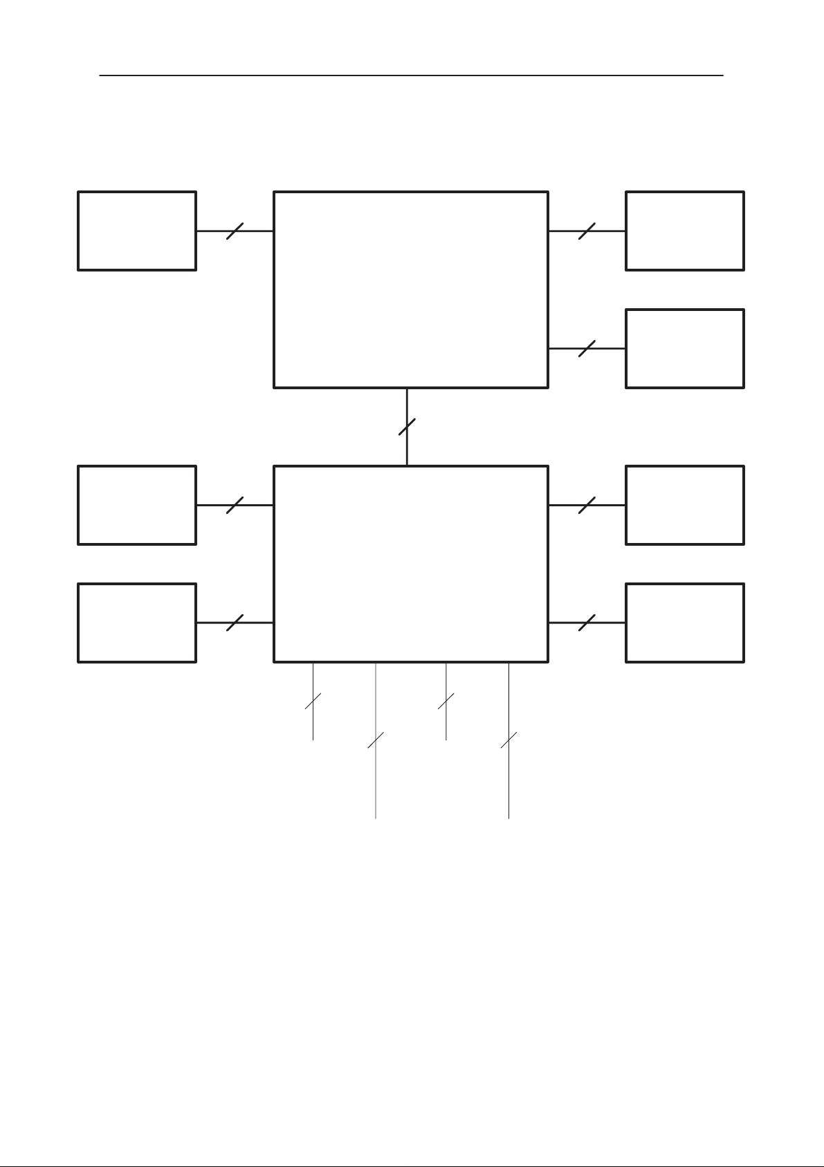
Interconnection Diagram
19 9
Technical Documentation
Keypad Display
User Interface
Module
UE4
28
6
SIM Battery
2
Earpiece
4
System/RF
Antenna
1
System
Connector
(including Mic)
Connector
Module
UR9U
2
Charger
RF
2
Side keys
3 + 36+2
2
IR
Link
Page 3 – 6
Original 05/98
Page 7
PAMS
NSK–3
Technical Documentation
System Module
External and Internal Connectors
B side view
Fixing pads (2 pcs)
System Module
IBI connector
(6 pads)
8
1
7
14
Engine PCB
A side view
DC Jack
acoustic ports
Charger pads (3 pcs)
Microphone
Bottom
connector (6 pads)
Cable locking holes (3 pcs)
Cavity for microphone
Original 05/98
Page 3 – 7
Page 8
NSK–3
PAMS
System Module
Technical Documentation
System Connector Signals
Pin Name Function Description
1 V_IN Bottom charger contacts Charging voltage.
2 L_GND DC Jack Logic and charging ground.
3 V_IN DC Jack Charging voltage.
4 CHRG_CTRL DC Jack Charger control.
5 CHRG_CTRL Bottom charger contacts Charger control.
6 MICP Microphone Microphone signal, positive node.
7 MICN Microphone Microphone signal, negative node.
8 XMIC Bottom & IBI connectors Analog audio input.
9 SGND Bottom & IBI connectors Audio signal ground.
10 XEAR Bottom & IBI connectors Analog audio output.
11 MBUS Bottom & IBI connectors Bidirectional serial bus.
12 FBUS_RX Bottom & IBI connectors Serial data in.
13 FBUS_TX Bottom & IBI connectors Serial data out.
14 L_GND Bottom charger contacts Logic and charging ground.
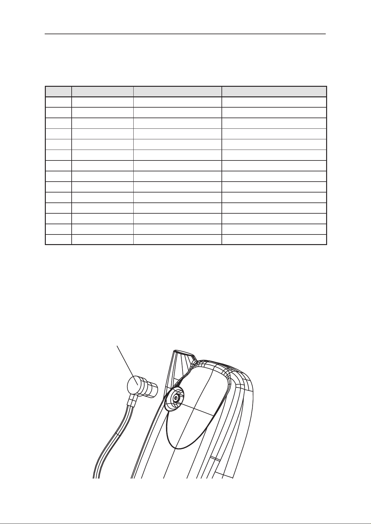
RF–Connector
The RF–connector is needed to utilize the external antenna with Car
Cradle. The RF–connector is located on the back side of the transceiver
on the top section. The connector is plug type connector with special mechanical switching.
Accessory side of connector
Part will be floating in
car holder
Phone side of connector
Page 3 – 8
Original 05/98
Page 9
PAMS
NSK–3
Technical Documentation
Battery Contacts
Pin Name Function Description
1 BVOLT Battery voltage Battery voltage
2 BSI Battery Size Indicator Input voltage
3 BTEMP Battery temperature indication
Phone power up
Battery power up
PWM to VIBRA BA TTERY
4 BGND Ground
Input voltage
Input voltage
Output voltage
PWM output signal frequency
SIM Reader
System Module
Original 05/98
Page 3 – 9
Page 10
NSK–3
PAMS
System Module
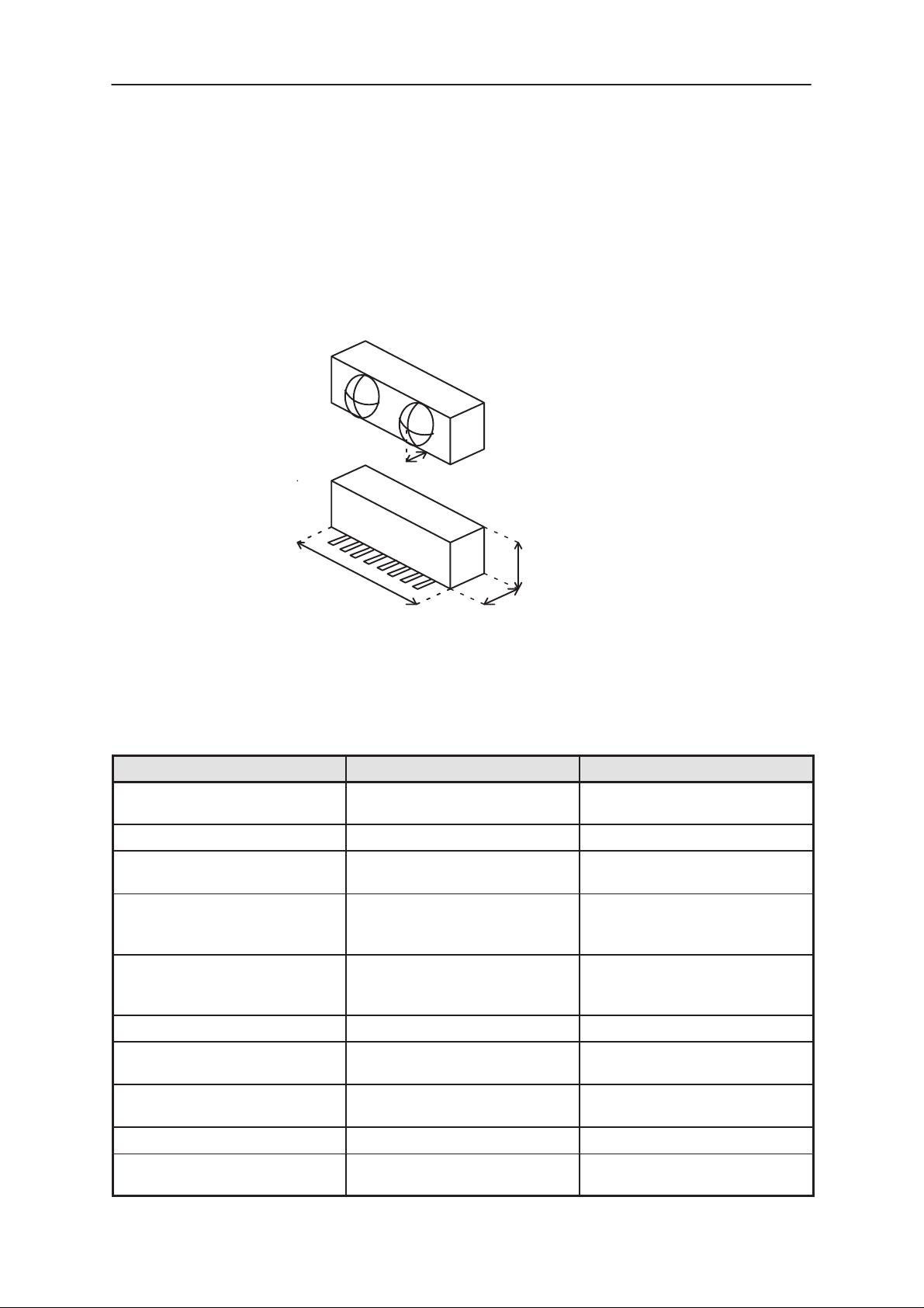
IR Link
IR link module is located into the top of the phone under the IR lens, see
Figure 2, Infra Red.
IR link is used as a data link to a PC or for transfering data between
phones
FRONT
BACK
Technical Documentation
2mm
4mm
10mm
3mm
Operating Conditions
Environmental condition Ambient temperature Notes
Normal operation conditions +7 oC ... +40 oC Specifications fulfilled and fast
charging possible
Extreme operation conditions –10 oC ... +55 oC Specifications fulfilled
Reduced performance condi-
tions
Intermittent operation condi-
tions
Cessation of operation <–25 oC and >80 oC No storage or operation at-
Long term storage conditions 0 oC ... +40 oC Battery only up to +30 oC !
+55 oC ... +65 oC Operational only for short peri-
ods
–25 oC ... –10 oC and
+65 oC ... +80 oC
Operation maybe not possible
but attempt to operate will
not damage the phone
tempt possible without per-
manent dam– age
Short term storage, max. 96 h –25 oC ... +70 oC Cumulative for life–time of bat-
tery
Short term storage, max. 12 h –25 oC ... +80 oC Cumulative for life–time of bat-
tery
–25 oC ... +75 oC LCD operation
Short term operation > +70 oC Maximum value for SIM card,
GSM spec. 11.11
Page 3 – 10
Original 05/98
Page 11

PAMS
NSK–3
Technical Documentation
Functional Description
The DCS 1800 engine consist of a Baseband/RF module with connections to a separate user interface module. Baseband and RF modules
are interconnected with PCB wiring. The engine can be connected to accessories via the bottom system connector, the Intelligent Battery Interface (IBI) connector and IR–link.
The RF submodule receives and demodulates radio frequency signals
from the base station and transmits modulated RF signals to the base
station. It consists of functional submodules Receiver, Frequency Synthesizer and Transmitter.
The Baseband module containes audio, control, signal processing and
power supply functions. It consists of functional submodules CTRLU
(Control Unit; MCU, DSP, logic and memories), PWRU (Power Supply;
regulators and charging) and AUDIO_RF (audio coding, RF–BB interface).
System Module
Modes of Operation
UR4 operates in cellular mode and a local mode for service:
– Cellular mode, phone controlled by OS and partly by basestation
– Locals mode, used by Production and After Sales.
– Acting Dead mode
– Power Off mode
– Flash mode
Cellular Mode
In cellular mode phone performes all the tasks to place and release calls.
Also charging and communication between accessories and phone are
done during this mode by OS. Signaling and handover functions are supported by basestation.
Power off
In the power–off mode only CCONT is active. Power–off mode can be left
by pushing the PWR–key, connecting charger to the phone, real time
clock interrupt or intelligent battery interrupt.
Locals Mode
Locals mode is used for testing purposes by Product Development, Production and After Sales. The Cellular Software is stopped (no signalling
to base station), and the phone is controlled by MBUS/FBUS messages
by the controlling PC.
Original 05/98
Page 3 – 11
Page 12
NSK–3
PAMS
System Module
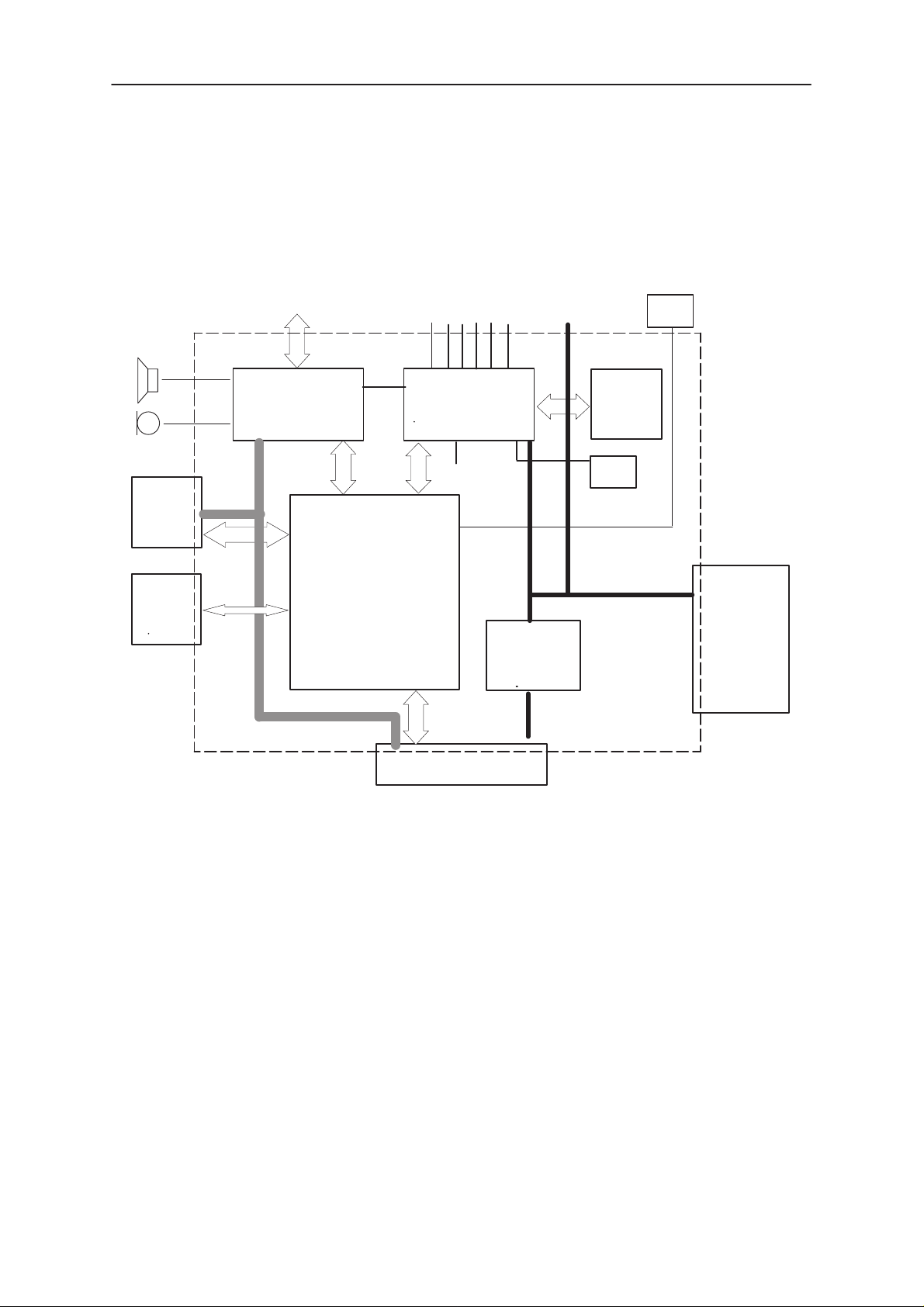
Baseband Module
Block Diagram
TX/RX SIGNALS
COBBA
UI
COBBA SUPPLY
RF SUPPLIES
CCONT
BB SUPPLY
Technical Documentation
PA SUPPLY
32kHz
CLK
SLEEP CLOCK
SIM
13MHz
CLK
SYSTEM CLOCK
MAD
+
MEMORIES
IR
AUDIOLINES
BASEBAND
CHAPS
SYSCON
VBAT
BATTERY
Page 3 – 12
Original 05/98
Page 13
PAMS
NSK–3
Technical Documentation
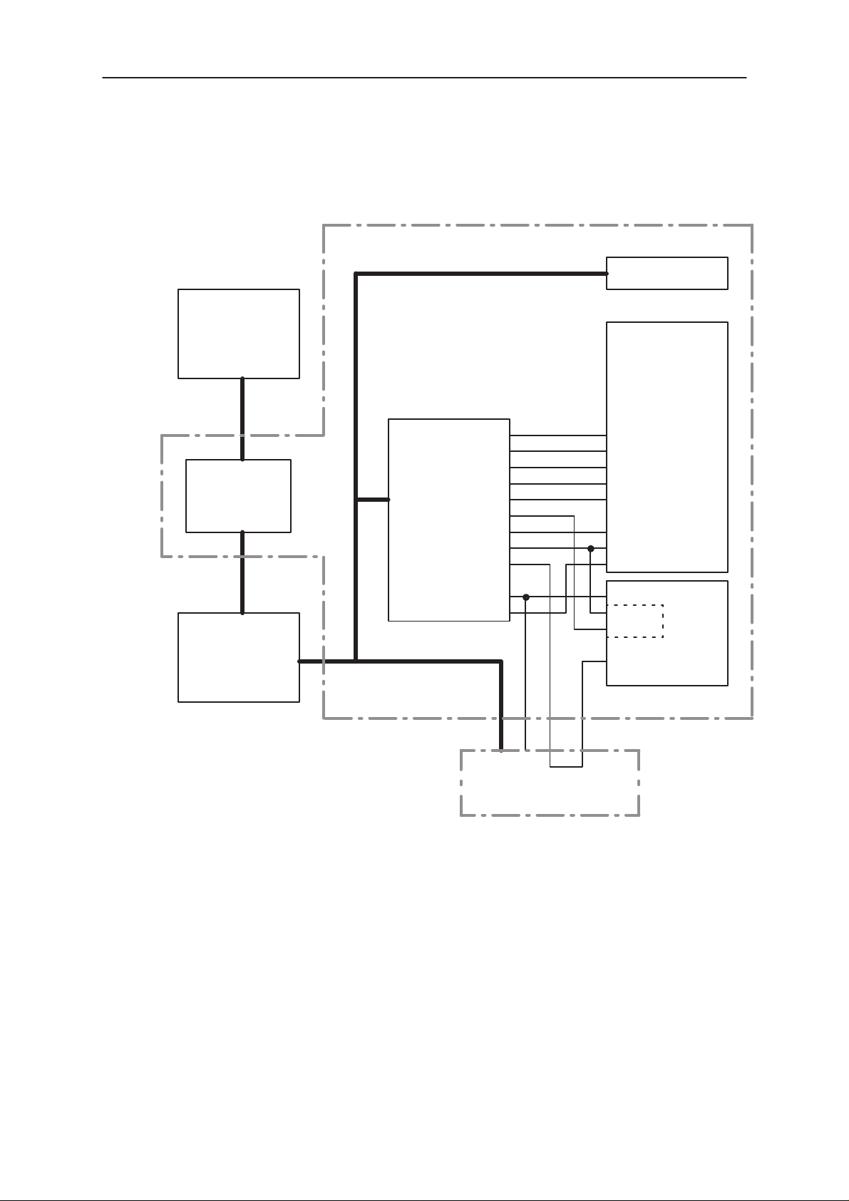
Power Distribution Diagram
Charger
Charge
control
UR4 engine
CCONT
System Module
VBAT
TX PA
RF
1800
VR1
VR2
VR3
VR4
VR5
VR6
VR7
VREF
Battery
VSIM
VBB
V5V
UI Module
Baseband
COBBA
analog
Original 05/98
Page 3 – 13
Page 14
NSK–3
PAMS
System Module
Technical Documentation
External interfaces
Antenna
4
Battery
Pack
3
Charger
IBI
Connector Name Code Notes
Bottom & IBI connector 5469061 Includes DC plug and microphone connec-
User Interface Module connector 5460021 28 pins, spring contacts.
UR4
ENGINE
6
Bottom
connectorconnector
SIM
6
Mic
tions.
28
User
Interface
Module
Display
Keyboard
Backlights
Speaker
Buzzer
Battery connector 5469069 2 pieces, 2 connections each.
SIM connector 5400085 Supports 3V/5V SIM cards
Flash Programming connector
The system connector can be used as a flash prom programming interface for
flash memories for updating (i.e. re–programming) the flash program memory.
The phone has to be switched off, when the flash prommer is connected to the
phone system connector. The baseband is powered up as the supply voltage
is connected to the charger contacts, or by pressing the PWR button, or by an
IBI device..
The program execution starts from the BOOT ROM and the MCU investigates
in the early start–up sequence if the flash prommer is connected. This is done
by checking the status of the MBUS–line. Normally this line is high but when
the flash prommer is connected the line is forced low by the prommer. The
flash prommer serial data receive line is in receive mode waiting for an acknowledgement from the phone. The data transmit line from the baseband to
the prommer is initially high. When the baseband has recognized the flash
prommer, the TX–line is pulled low. This acknowledgement is used to start the
data transfer of the first two bytes from the flash prommer to the baseband on
the RX–line. The data transmission begins by starting the serial transmission
clock (MBUS–line) at the prommer.
The 5V programming voltage is supplied inside the transceiver from the battery
voltage with a switch mode regulator (5V/30mA) of the CCONT. The voltage is
fed via UI connector to avoid damage of the CCONT during production line
flasing ( 12V fed to FLASH Vpp from the production tester ).
Page 3 – 14
Original 05/98
Page 15
PAMS
NSK–3
Technical Documentation
Pin Name Parameter Min Typ Max Unit Remark
1 VIN Supply
Voltage
11 MBUS Serial clock
from the
Prommer
12 FBUS_RX Serial data
from the
Prommer
13 FBUS_TX Data ac-
knowledge to
the Prommer
13 GND GND 0 0 V Supply ground
6.8 7.8 8.8 V Supply Voltage,Current li-
2.0
0
2.0
0
2.0
0
2.8
0.8
2.8
0.8
2.8
0.8
V Prommer detection and
V Receive Data from
V Transmit Data from Base-
System Module
mitted to 850 mA
Serial Clock for synchro-
nous communication
Prommer to Baseband
band to Prommer
Battery connector
The BSI contact on the battery connector is used to detect when the battery is to be removed to be able to shut down the operations of the SIM
card before the power is lost if the battery is removed with power on. The
BSI contact in the battery pack should be shorter than the supply power
contacts to give enough time for the SIM shut down.
A vibra alerting device is used for giving silent signal to the user of an incoming call. The device is not placed in the phone but it will be added to a
special battery pack. The vibra is controlled with a PWM signal by the
MAD via the BTEMP battery terminal.
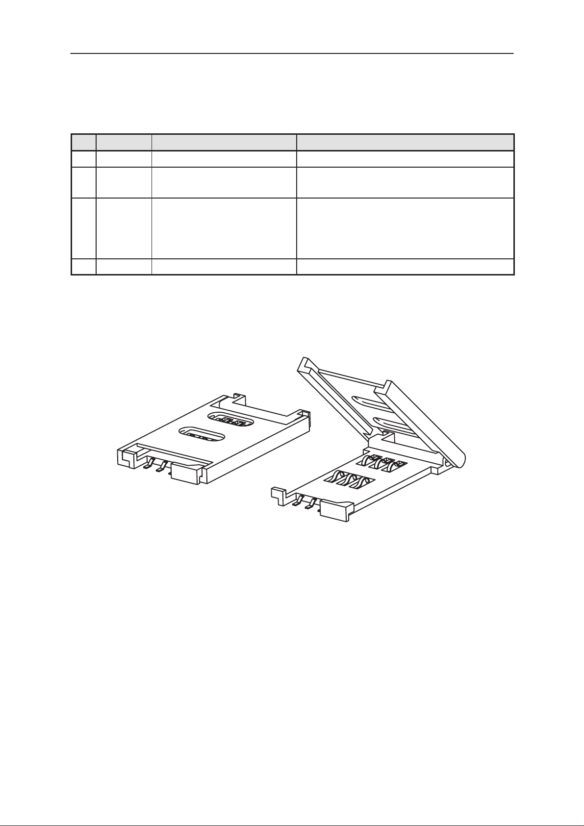
SIM card connector
Pin Name Parameter Min Typ Max Unit Notes
1 GND GND 0 0 V Ground
2 VSIM 5V SIM Card
3V SIM Card
3 DATA 5V Vin/Vout
3V Vin/Vout
4 SIMRST 5V SIM Card
3V SIM Card
5 SIMCLK Frequency
Trise/Tfall
4.8
2.8
4.0
0
2.8
0
4.0
2.8
1.625 3.25 5.0
5.0
3.0
”1”
”0”
”1”
”0”
”1”
”1”
5.2
3.2
VSIM
0.5
VSIM
0.5
VSIM
VSIM
25
V Supply voltage
V SIM data
Trise/Tfall max 1us
V SIM reset
MHz
ns
SIM clock
Original 05/98
Page 3 – 15
Page 16
NSK–3
PAMS
System Module
Infrared transceiver module
An infrared transceiver module is designed to substitute an electrical
cable between the phone and a PC. The infrared transceiver module is a
stand alone component capable to perform infrared transmitting and receiving functions by transforming signals transmitted in infrared light from
and to electrical data pulses running in two wire asyncronous databus. In
NSK–3 the module is placed inside the phone at the top of the phone.
The module is activated with an IRDASD signal by the MAD, which pulls
low the shut down pin of the module (standby current in shut down mode
is specified to 10uA maximum). The RX and TX signals are connected to
the MAD accessory interface AccIf via FBUS. The AccIf in MAD performs
pulse encoding and shaping for transmitted data and detection and decoding for received data pulses.
The data is transferred over the IR link using serial FBUS data at speeds
9.6, 19.2, 38.4, 57.6 or 115.2 kbits/s, which leads to maximum throughput
of 92.160 kbits/s. The used IR module complies with the IrDA SIR specification (Infra Red Data Association), which is based on the HP SIR (Hewlett–Packard‘s Serial Infra Red) consept.
Technical Documentation
the following figure gives an example of IR transmission pulses. In IR
transmission a light pulse correspondes to 0–bit and a ”dark pulse” correspondes to 1–bit.
constant pulse
IR TX
UART TX
startbit stopbit1 0100110
The FBUS cannot be used for external accessory communication, when
the infrared mode is selected. Infrared communication reserves the FBUS
completely.
Page 3 – 16
Original 05/98
Page 17

PAMS
NSK–3
Technical Documentation
Real time clock
Requirements for a real time clock implementation are a basic clock
(hours and minutes), a calender and a timer with alarm and power on/off
–function and miscellaneous calls. The RTC will contain only the time
base and the alarm timer but all other functions (e.g. calendar) will be implemented with the MCU software. The RTC needs a power backup to
keep the clock running when the phone battery is disconnected. The
backup power is supplied from a rechargable polyacene battery that can
keep the clock running some ten minutes. If the backup has expired, the
RTC clock restarts after the main battery is connected. The CCONT
keeps MCU in reset until the 32kHz source is settled (1s max).
The CCONT is an ideal place for an integrated real time clock as the asic
already contains the power up/down functions and a sleep control with
the 32kHz sleep clock, which is running always when the phone battery is
connected. This sleep clock is used for a time source to a RTC block.
System Module
Signals between baseband and User Interface section
The User interface section is implemented on separate UI board, which
connects to the engine board with a board to board spring connector.
User Interface module connection
The User interface section comprises the keyboard with keyboard lights,
display module with display lights, an earphone and a buzzer.
Earphone
The internal earphone is connected to the UI board by means of mounting springs for automatic assembly. The low impedance, dynamic type
earphone is connected to a differential output in the COBBA audio codec.
The electrical specifications for the earphone output are shown in
NO TAG. The voltage level at each output is given as reference to
ground. Earphone levels are given to 32 ohm load.
Buzzer
Alerting tones and/or melodies as a signal of an incoming call are generated with a buzzer that is controlled with a PWM signal by the MAD. Also
keypress and user function response beeps are generated with the buzzer. The buzzer is a SMT device and is placed on the UI board.
Original 05/98
Page 3 – 17
Page 18
NSK–3
PAMS
System Module
Power Distribution
In normal operation the baseband is powered from the phone‘s battery.
The battery consists of one Lithium–cell. There is also a possibility to use
batteries consisting of three Nickel– cells. An external charger can be
used for recharging the battery and supplying power to the phone. The
charger can be either so called fast charger, which can deliver supply current up to 850 mA or a standard charger that can deliver around 300 mA.
The baseband contains components that control power distribution to
whole phone excluding the power amplifier, which have a continuous
power rail direct from the battery. The battery feeds power directly to
three parts of the system: CCONT, power amplifier, and UI (buzzer and
display and keyboard lights).
The power management circuitry provides protection agains overvoltages, charger failures and pirate chargers etc. that would otherwise
cause damage to the phone. The circuitry is implemented in the beginning with discrete components, but it will be partly or fully integrated on
later phase.
Technical Documentation
PA SUPPLY
VCOBBA
COBBA
UI
VBAT
VBB
MAD
+
MEMORIES
BASEBAND
RF SUPPLIES
CCONT
PWRONX
CNTVR
VBB
PURX
V2V
CONNECTOR
POWER
MGMT
VIN
VSIM
VBAT
PWM
SIM
RTC
BACKUP
BATTERY
The heart of the power distrubution is the CCONT. It includes all the voltage regulators and feeds the power to the whole system. The whole
baseband is powered from the same regulator which provides 2.8V baseband supply VBB. The baseband regulator is active always when the
phone is powered on. The baseband regulator feeds MAD and memories,
COBBA digital parts and the LCD driver in the UI section. There is a separate regulator for a SIM card.
Page 3 – 18
Original 05/98
Page 19
PAMS
NSK–3
Technical Documentation
The regulator is selectable between 3V and 5V and controlled by the
SIMPwr line from MAD to CCONT. SIM card regulator is also used for after sales flash programming. COBBA analog parts are powered from a
dedicated 2.8V supply VCOBBA by the CCONT. The CCONT supplies
also 5V for RF. The CCONT contains a real time clock function, which is
powered from a RTC backup when the main battery is disconnected. The
RTC backup is rechargable polyacene battery.
CCONT includes also six additional 2.8V regulators providing power to
the RF section. These regulators can be controlled either by the direct
control signals from MAD or by the RF regulator control register in
CCONT which MAD can update. Below are the listed the MAD control
lines and the regulators they are controlling.
– TxPwr controls VTX regulator (VR7)
– RxPwr controls and VRX regulators (VR2 and VR5)
– SynthPwr controls VSYN_A and VSYN_D regulators (VR4 and VR3)
– VCXOPwr controls VXO and VCOBBA regulators (VR1 and VR6)
System Module
CCONT generates also a 1.5 V reference voltage VREF to COBBA,
PLUSSA and CRFU. The VREF voltage is also used as a reference to
some of the CCONT A/D converters.
In additon to the above mentioned signals MAD includes also TXP control
signal which goes to PLUSSA power control block and to the power amplifier. The transmitter power control TXC is led from COBBA to PLUSSA.
Regulator Max.current Unit Vout Unit Notes
VR1 25 mA 2.8 V VVCXO
VR2 25 mA 2.8 V NOT USED
VR3 50 mA 2.8 V VSYN_D
VR4 90 mA 2.8 V VSYN_A
VR5 80 mA 2.8 V VRX
VR6 100 mA 2.8 V COBBA
VR7 150 mA 2.8 V VTX .Depends on exter
nal BJT
V2V 50 mA 1.3 –
2.65
V MAD core voltage, in
225mV steps (1.975V
default)
VBB ON
VBB SLEEP
VSIM 30 mA 3.0/
V5V 30 mA 5.0 V for RF
Original 05/98
125
1
mA
mA
2.8
2.8
5.0
V current limit 250mA
current limit 5mA
V VSIM output voltage
selectable,Used also for
flashing. (VPP)
Page 3 – 19
Page 20

NSK–3
PAMS
System Module
Power up
The baseband is powered up by:
Technical Documentation
1. Pressing the power key, that generates a PWRONX interrupt
signal from the power key to the CCONT, which starts the power up procedure.
2. Connecting a charger to the phone. The CCONT recognizes
the charger from the VCHAR voltage and starts the power up
procedure.
Before battery voltage voltage rises over 3.0 V Charging Logic
gives an initial charge (with limited current) to the battery. After
battery voltage reaches that voltage limit the power up procedure is as described in the previous chapters.
3. A RTC interrupt. If the real time clock is set to alarm and the
phone is switched off, the RTC generates an interrupt signal,
when the alarm is gone off. The RTC interrupt signal is connected to the PWRONX line to give a power on signal to the
CCONT just like the power key.
When the CCONT is activated, it swithes on the baseband supply voltage
and generates a power up reset signal PURX to the MAD. When the
PURX reset is released, the MAD releases the system reset ExtSysReset
and the internal MCUResetX signals and starts the boot program execution. If booting is succeeded program execution continues from flash program memory. When the phone is powered up with an empty battery pack
using the standard charger, the charger may not supply enough current
for standard powerup procedure and the powerup must be delayed.
Acting Dead
If the phone is off when the charger is connected, the phone is powered
on but enters a state called ”acting dead”. To the user the phone acts as if
it was switched off. A battery charging alert is given and/or a battery
charging indication on the display is shown to acknowledge the user that
the battery is being charged.
4. A battery interrupt. Intelligent battery packs have a possibility
to power up the phone. When the battery gives a short (10ms)
voltage pulse through the BTEMP pin, the CCONT wakes up
and starts the power on procedure.
Active Mode
In the active mode the phone is in normal operation, scanning for channels, listening to a base station, transmitting and processing information.
All the CCONT regulators are operating. There are several substates in
the active mode depending on if the phone is in burst reception, burst
transmission, if DSP is working etc..
Page 3 – 20
Original 05/98
Page 21

PAMS
NSK–3
Technical Documentation
Sleep Mode
In the sleep mode all the regulators except the baseband VBB and the
SIM card VSIM regulators are off. Sleep mode is activated by the MAD
after MCU and DSP clocks have been switched off. The voltage regulators for the RF section are switched off and the VCXO power control,
VCXOPwr is set low. In this state only the 32 kHz sleep clock oscillator in
CCONT is running. The flash memory power down input is connected to
the VCXO power control, so that the flash is deep powered down during
sleep mode.
The sleep mode is exited either by the expiration of a sleep clock counter
in the CCONT or by some external interrupt, generated by a charger connection, key press, headset connection etc. The MAD starts the wake up
sequence and sets the VCXOPwr control high. After VCXO settling time
other regulators and clocks are enabled for active mode.
If the battery pack is disconnect during the sleep mode, the CCONT
should power down the SIM in the sleep mode as there is no time to wake
up the MCU.
System Module
Charging
The power management circuitry controls the charging current delivered
from the charger to the battery. Charging is controlled with a PWM input
signal, generated by the CCONT. The PWM pulse width is controlled by
the MAD and sent to the CCONT through a serial data bus. The battery
voltage rise is limited to a specified level by turning the switch off. Charging current is passed through protection ASIC CHAPS and monitored by
measuring the voltage drop across a 220mohm resistor.
2–wire charging
With 2–wire charging the charger provides constant output current, and
the charging is controlled by PWMOUT signal from CCONT to Charging
Logic. PWMOUT signal frequency is selected to be 1 Hz, and the charging switch in Charging Logic is pulsed on and off at this frequency. The
final charged energy to battery is controlled by adjusting the PWMOUT
signal pulse width.
Both the PWMOUT frequency selection and pulse width control are made
MCU which writes these values to CCONT.
3–wire charging
With 3–wire charging the charger provides adjustable output current, and
the charging is controlled by PWMOUT signal from CCONT to Charger,
with the bottom connector signal. PWMOUT signal frequency is selected
to be 32 Hz, and the charger output current is controlled by adjusting the
PWMOUT signal pulse width. The charger switch in Charging Logic is
constantly on in this case.
Original 05/98
Page 3 – 21
Page 22

NSK–3
PAMS
System Module
Power Off
The baseband is powered down by:
The power down is controlled by the MAD. When the power key has been
pressed long enough or the battery voltage is dropped below the limit the
MCU initiates a power down procedure and disconnects the SIM power.
Then the MCU outputs a system reset signal and resets the DSP. If there
is no charger connected the MCU writes a short delay to CCONT watchdog and resets itself. After the set delay the CCONT watchdog expires,
which activates the PURX and all regulators are switched off and the
phone is powered down by the CCONT.
Technical Documentation
1. Pressing the power key, that is monitored by the MAD, which
starts the power down procedure.
2. If the battery voltage is dropped below the operation limit, either by not charging it or by removing the battery.
3. Letting the CCONT watchdog expire, which switches off all
CCONT regulators and the phone is powered down.
4. Setting the real time clock to power off the phone by a timer.
The RTC generates an interrupt signal, when the alarm is gone
off. The RTC interrupt signal is connected to the PWRONX line
to give a power off signal to the CCONT just like the power key.
If a charger is connected when the power key is pressed the phone enters into the acting dead mode.
Audio control
The audio control and processing is taken care by the COBBA, which
contains the audio and rf codecs, and the MAD, which contains the MCU,
ASIC and DSP blocks handling and processing the audio signals.
Microphone and Earphone
The baseband supports three microphone inputs and two earphone outputs. The inputs can be taken from an internal microphone, a headset microphone or from an external microphone signal source. The microphone
signals from different sources are connected to separate inputs at the
COBBA asic. Inputs for the microphone signals are differential type.
The output for the internal earphone is a dual ended type output capable
of driving a dynamic type speaker. The output for the external accessory
and the headset is single ended with a dedicated signal ground SGND.
Input and output signal source selection and gain control is performed inside the COBBA asic according to control messages from the MAD. Keypad tones, DTMF, and other audio tones are generated and encoded by
the MAD and transmitted to the COBBA for decoding.
Page 3 – 22
Original 05/98
Page 23

PAMS
NSK–3
Technical Documentation
Speech processing
The speech coding functions are performed by the DSP in the MAD and
the coded speech blocks are transferred to the COBBA for digital to analog conversion, down link direction. In the up link direction the PCM coded
speech blocks are read from the COBBA by the DSP.
There are two separate interfaces between MAD and COBBA: a parallel
bus and a serial bus. The parallel bus has 12 data bits, 4 address bits,
read and write strobes and a data available strobe. The parallel interface
is used to transfer all the COBBA control information (both the RFI part
and the audio part) and the transmit and receive samples. The serial interface between MAD and COBBa includes transmit and receive data,
clock and frame synchronisation signals. It is used to transfer the PCM
samples. The frame synchronisation frequency is 8 kHz which indicates
the rate of the PCM samples and the clock frequency is 1 MHz. COBBA is
generating both clocks.
System Module
Alert Signal Generation
A buzzer is used for giving alerting tones and/or melodies as a signal of
an incoming call. Also keypress and user function response beeps are
generated with the buzzer. The buzzer is controlled with a BuzzerPWM
output signal from the MAD. A dynamic type of buzzer must be used
since the supply voltage available can not produce the required sound
pressure for a piezo type buzzer. The low impedance buzzer is connected
to an output transistor that gets drive current from the PWM output. The
alert volume can be adjusted either by changing the pulse width causing
the level to change or by changing the frequency to utilize the resonance
frequency range of the buzzer.
A vibra alerting device is used for giving silent signal to the user of an incoming call. The device is controlled with a VibraPWM output signal from
the MAD. The vibra alert can be adjusted either by changing the pulse
width or by changing the pulse frequency. The vibra device is not inside
the phone, but in a special vibra battery.
Original 05/98
Page 3 – 23
Page 24

NSK–3
PAMS
System Module
Digital control
MAD
The baseband functions are controlled by the MAD asic, which consists of
a MCU, a system ASIC and a DSP. The DCS/PCN specific asic is named
as MAD2. There are separate controller asics in TDMA and JDC named
as MAD1 and MAD3. All the MAD asics contain the same core processors and similar building blocks, but differ from each other in system specific functions, pinout and package types.
MAD2 contains following building blocks:
– ARM RISC processor with both 16–bit instruction set (THUMB mode)
and 32–bit instruction set (ARM mode)
– TMS320C542 DSP core with peripherials:
Technical Documentation
– API (Arm Port Interface memory) for MCU–DSP commu-
nication, DSP code download, MCU interrupt handling vec-
tors (in DSP RAM) and DSP booting
– Serial port (connection to PCM)
– Timer
– DSP memory (80 kW RAM in PD version of MAD2)
– BUSC (BusController for controlling accesses from ARM to API, Sys-
tem Logic and MCU external memories, both 8– and 16–bit memories)
– System Logic
– CTSI (Clock, Timing, Sleep and Interrupt control)
– MCUIF (Interface to ARM via B
tROM
– DSPIF (Interface to DSP)
– MFI (Interface to COBBA AD/DA Converters)
– CODER (Block encoding/decoding and A51&A52 ciphering)
– AccIF(Accessory Interface)
– SCU (Synthesizer Control Unit for controlling 2 separate
synthesizer)
USC). Contains MCU Boo-
Page 3 – 24
– UIF (Keyboard interface, serial control interface for COBBA
PCM Codec, LCD Driver and CCONT)
– SIMI (SimCard interface with enhanched features)
– PUP (Parallel IO, USART and PWM control unit for vibra
and buzzer)
Original 05/98
Page 25

PAMS
NSK–3
Technical Documentation
The MAD operates from a 13 MHz system clock, which is generated from
the 13Mhz VCXO frequency. The MAD supplies a 6,5MHz or a 13MHz
internal clock for the MCU and system logic blocks and a 13MHz clock for
the DSP, where it is multiplied to 52 MHz DSP clock. The system clock
can be stopped for a system sleep mode by disabling the VCXO supply
power from the CCONT regulator output. The CCONT provides a 32kHz
sleep clock for internal use and to the MAD, which is used for the sleep
mode timing. The sleep clock is active when there is a battery voltage
available i.e. always when the battery is connected.
Memories
The MCU program code resides in an external program memory. MCU
work (data) memory size is either 512kbits or 1Mbits. A serial EEPROM
is used for storing the system and tuning parameters, user settings and
selections, a scratch pad and a short code memory. The EEPROM size
is 64kbits. The memory variation is managed using memory components
with the same packages and pinouts for all memory sizes of the given
types. The system parameters contain information of the used memories
in that end product. The selected memory packages are TSOP48 for
ROM, STSOP32 for RAM and SO8S for EEPROM .
System Module
The used flash memories are capable to perform erase and write operations with the supplied 5V ( 3V ) programming voltage.
The BusController (BUSC) section in the MAD decodes the chip select
signals for the external memory devices and the system logic. BUSC controls internal and external bus drivers and multiplexers connected to the
MCU data bus. The MCU address space is divided into access areas with
separate chip select signals. BUSC supports a programmable number of
wait states for each memory range.
Program Memory
The MCU program code resides in the program memory. The program
memory size is 8Mbits (512kx16) The default package is TSOP48.
The power down pin of FLASH is utilized in the system sleep mode by
connecting the VCXOPwr to the flash power down pin to minimize the
flash power consumption during the sleep.
Original 05/98
Page 3 – 25
Page 26

NSK–3
PAMS
System Module
SRAM Memory
The work memory size can vary depending on the product variation similarily to the program memory. The work memory is a static ram of size
512kbits (64kx8) or 1Mbits (128kx8). The work memory is supplied from
the common baseband VBB voltage and the memory contents are lost
when the baseband voltage is switched off. All retainable data should be
stored into the EEPROM when the phone is powered down.
EEPROM Memory
An EEPROM is used for a nonvolatile data memory to store the tuning
parameters and phone setup information. The short code memory for
storing user defined information is also implemented in the EEPROM.
The EEPROM size is 8kbytes .The memory is accessed through a serial
bus and the default package is SO8S.
MCU Memory Map
Technical Documentation
MAD supports maximum of 4GB internal and 4MB external address
space. External memories use address lines MCUAd0 to MCUAd21 and
8–bit/16–bit databus. The BUSC bus controller supports 8– and 16–bit
access for byte, double byte, word and double word data. Access wait
states (0, 1 or 2) and used databus width can be selected separately for
each memory block.
Page 3 – 26
Original 05/98
Page 27

PAMS
NSK–3
Technical Documentation
Baseband EMC Strategy
The baseband EMC strategy is divided into electrical and mechanical
items. As electrical guide lines, clocks and high speed signals should be
routed in inner layers and away from the PCB edges. Clock signals distributed to other circuits should have series resistors incorporated to reduce rise times and reflections. Slew rate controlled buffers should be
used on custom components wherever possible to reduce the EMC produced by the circuit. Separate power supplies for digital, analog and rf–
blocks should be used as much as possible. Baseband and RF supply
power rails should be isolated from each other by means of inductors in
the power supply rail to prevent high frequency components produced on
the baseband power supply rail to spread out over the RF power supply
plane. This might be required to avoid interference from digital circuits to
affect the performance of RF section.
All external connectors and connection must be filtered using RC or LC
networks to prevent the high frequency components from entering connection cables that then will act as antennas. The amount of this type of
EMC component is in straight relation to the amount of external connections. The type of network and amount of components to be used is determined by the AC and DC impedance characteristic of that particular
signal. Low impedance signals requires LC network while medium impedance level signals, input signals at moderate band width can use RC networks.
System Module
The EMC protection should also prevent external or internal signals to
cause interference to baseband and in particular to audio signals. Internal
interference is generated by the transmitter TDMA frequency and the
switchmode charging. The transmitter TDMA frequency interference is
likely to cause noise to both microphone and earphone signals. The
transmitter RF interference is likely to cause more problems in the microphone circuitry than in the earphone circuitry since the earpiece is a low
impedance dynamic type.
As mechanical guide lines, the baseband and RF sections should be isolated from each other using EMC shielding, which suppresses radiated
interferences. The transmitter TDMA frequency can also generate mechanical vibrations that can be picked up by the microphone if it is not
properly isolated from the chassis using rubber or some other soft material. A spring connected microphone is used to prevent microphone interference problems. Connection wires to internal microphone and earphone
should be as short as possible to reduce the interference caused by internal signals.
ESD protection has to be implemented on each external connection that
is accessable during normal operation of the phone.
Original 05/98
Page 3 – 27
Page 28

NSK–3
PAMS
System Module
RF Module
RF Frequency Plan
RX
1805.2–1879.8
LO–
buffers
1st IF 487
2nd LO 400
UHF
VCO
RX=1318.2–1392.8
TX=1310.2–1384.8
2nd IF 87
3rd LO 100
Technical Documentation
f
f
f/2f/4
UHF
PLL
VHF
PLL
3rd IF 13
VHF
VCO
800
13 MHz
VCXO
TX
1710.2–1784.8
IF 400
CRFU2A
Note: 1 All frequencies are in MHz
2 Underlined frequencies are DCS1800
3 Bold frequencies are DCS1900
4 Other frequencies are common to both systems
DC Characteristics
Power Distribution Diagram
Current consumption of each regulator is shown in the following power
distribution diagram (Figure 2 shows maximum currents, Figure 3 shows
typical currents). On the left side of the figure, are the regulator control
signals. Above each regulator is the rated current for that regulator. The
name on the right side of the regulator block (smaller font) indicates the
signal name used on the schematics. On the far right side of the figure
are the pin names (power) for the different ICs.
MOD.
PLUSSA
I and Q
Page 3 – 28
Original 05/98
Page 29

PAMS
NSK–3
Technical Documentation
Power Distribution – Maximum Currents
VCXOEN
RXPWR
SYNPWR
1mA
VR1 VCTCXO
VVCXO
2mA
36.6mA
VR5
VRX
4mA
13mA
29mA
10.2mA
VSYN_D
11mA
VR3
2mA
VCTCXO buffer
Receiver
LNA
RX mixer UHF
VHF buffer + mix2
VHF predivider
UHF predivider
Dividers
System Module
PLUSSA (VRX)
CRFU2a (V_RX)
CRFU2a (V_VHF)
PLUSSA (VP1)
PLUSSA (VP2)
PLUSSA (VDD)
TXPWR
VR4
VR2
V5V
150 mA
VR7
External
transistor
VSYN_A
VDET
V5V
VTX
25mA
7mA
14mA
1.6mA
0.6mA
0.6mA
70mA
37.5mA
2.65mA
15mA
70mA
UHF VCO + buffer
VHF VCO
UHF buffer RX+TX
detector/temp
charge pump
charge pump
PLUSSA (VCE1)
PLUSSA (VCE2)
TX upconverter
Transmitter
Pwrcntrl opamp
TX buffer
PA gain control
CRFU2a (V_UHF)
CRFU2a (V_TX)
PLUSSA (VTX)
PLUSSA (VOP)
VBAT
1.32A
battery TX PA
TXP
NOTE: Currents are only estimates at this time
Original 05/98
PA 45%
max. output
(32.5dBm)
Vbat=3.0V
Page 3 – 29
Page 30

NSK–3
PAMS
System Module
Power Distribution – Typical Currents
VCXOEN
RXPWR
SYNPWR
0.7mA
VR1 VCTCXO
VVCXO
1.0mA
31mA
VR5
VRX
3.3mA
13mA
18mA
7mA
VSYN_D
7mA
VR3
1.5mA
VCTCXO buffer
RX mixer UHF
VHF buffer + mix2
VHF predivider
UHF predivider
Receiver
LNA
Dividers
Technical Documentation
PLUSSA (VRX)
CRFU2a (V_RX)
CRFU2a (V_VHF)
PLUSSA (VP1)
PLUSSA (VP2)
PLUSSA (VDD)
TXPWR
VR4
VR4
V5V
150 mA
VR7
External
transistor
VSYN_A
VDET
V5V
VTX
20mA
7.6mA
9.1mA
0.8mA
0.5mA
0.5mA
49mA
32mA
2.4mA
14mA
UHF VCO + buffer
VHF VCO
UHF buffer RX+TX
detector/temp
charge pump
charge pump
TX upconverter
Transmitter
Pwrcntrl opamp
TX buffer
CRFU2a (V_UHF)
PLUSSA (VCE1)
PLUSSA (VCE2)
CRFU2a (V_TX)
PLUSSA (VTX)
PLUSSA (VOP)
TXP
Page 3 – 30
70mA
PA gain control
VBAT
1.1 A
battery TX PA
PA 45%
max. output
(32.5dBm)
Vbat=3.6V
Original 05/98
Page 31

PAMS
NSK–3
Technical Documentation
Functional Description
The following description of the RF is valid for both GSM 1800 and GSM
1900, the only differences between the two systems are:
1. antenna
2. duplexer (Z401)
3. RX and TX interstage filters (Z604 and Z503/Z505)
4. UHF VCO modules (G701)
5. matching networks (discrete components)
6. PA (N500)
Even though different components are used in the two engines, the footprints of the different components are the same. As can been seen from
the RF block diagram, most of the functions have been integrated into
three ASICs.
CRFU2a (N402) is a wideband UHF ASIC with both receiver and transmitter functions. The receiver functions include LNA bias and two downconversion mixers (Gilbert cell) with LO buffers. The LNA transistor is external to CRFU2a. The transmitter functions include an upconversion
mixer (image rejection) with LO buffer. All inputs/outputs are wideband
and require external matching networks for optimal performance.
System Module
PLUSSA (N401) provides two main functions:
1. RX/TX blocks
2. PLL
The receiver includes a Receive Controlled Gain Amplifier, a mixer with
LO buffers and IF amplifiers. The transmitter section includes a Transmit
Controlled Gain Amplifier, an I/Q Modulator, circuitry required to generate
the Quadrature Local Oscillator and Transmit Power Control which controls the MMIC PA (N500) output power. The PLL section is control via a
serial bus and contains both UHF and VHF PLL and predividers.
The MMIC PA (N500) uses gallium–arsenide heterojunction bipolar transistor (GaAs HBT) technology. The PA has an overall dynamic range of 45dB,
and is capable of producing 32.5dBm output power with +3dBm input.
Interfacing with the above ASICs is four more ASICs. These include:
1. CCONT (N100)– is a multifunction power management IC. This
ASIC contains six 2.8V linear regulators used in the RF section as well as
two 2.8V regulators used in the BB section. CCONT also contains a
switch mode supply power which generates +5V which is used to power
the charge pumps in PLUSSA. Some of the features of this IC are a nine
channel A/D converter, power up/down procedures, reset logic, charging
control, watchdog, sleep control and SIM interface.
world of the BB processing and the analog world of RF and audio circuitry.
Original 05/98
2. COBBA_GJ (N300)– is an interface between the digital
3. MAD2 (D200) – contains system logic and DSP
4. CHAPS (N110) – charging control ASIC
Page 3 – 31
Page 32

NSK–3
PAMS
System Module
Receiver
The receiver is a triple conversion receiver consisting of two ASICs;
CRFU2a (N402) and PLUSSA (N401). CRFU2a contains LNA bias circuitry with an external transistor which provides step gain depending on the
incoming RF level and the first and second mixers. PLUSSA contains the
third mixer. All filtering is external.
The received RF signal from the antenna is fed via the duplex filter (3
pole bandpass filter; Z401) to the LNA. Biasing and the AGC step circuitry are integrated into CRFU2a but the RF transistor, input and output
matching networks are external. The LNA gain step is controlled by
MAD2 (FRAC, D200). Gain step in LNA is activated when the receive RF
level is below –48 dBm. Following the LNA, the signal is fed to a 3 pole
ceramic bandpass filter (Z604). The combination of the duplex filter and
the bandpass filter define, the blocking characteristics of the receiver.
The bandpass filtered signal is fed back to CRFU2a, where the signal is
down converted with a double balanced active mixer (Gilbert cell) to 487
MHz. The local oscillator signal for this down conversion is generated by
the UHF VCO (G701) and buffered in CRFU2a. The first IF signal is
bandpass filtered with an discrete LC filter (L601, L602, L603, C605,
C606, C607 and C608), which also acts as a matching network. This filter attenuates the intermodulating and image frequencies. The second
down conversion (occurs in CRFU2a) results in a balanced IF of 87 MHz
which is filtered using an 87 MHz SAW filter (Z605). This filter provides
selectivity for channels greater than +/– 200 kHz, and attenuates the
image frequency of the third mixer and intermodulating signals. The local
oscillator signal for this down conversion is 400 MHz which is generated
by the 800 MHz VHF VCO module (G702). The VHF VCO signal is buffered and divided in PLUSSA and the 400 MHz resulting signal is again
buffered in CFRU2a before the mixer.
Technical Documentation
After the 87 MHz filter, the signal is fed into the AGC amplifier which has
been integrated into PLUSSA. The AGC amplifier contains analog gain
control which provides accurate gain control (minimum 60 dB) for the receiver. Control voltage for the AGC is generated by the D/A–converter in
COBBA_GJ (N300). The final mixing stage occurs in PLUSSA with a local oscillator signal of 100 MHz generated by dividing the VHF–synthesizer output (800 MHz) by eight.
The third (final) IF filter (Z606) is a ceramic bandpass filter with a centre
frequency of 13 MHz. This filter attenuates adjacent channels with very
little attenuation for +/– 200 kHz. The +/– 200 kHz interferers are filtered
digitally by DSP. The 13 MHz bandpass signal is converted to a balanced
signal with a buffer circuit in PLUSSA. This buffer circuit has a voltage
gain of 36 dB. This balanced signal is then fed to COBBA_GJ. The PGA
stage in COBBA_GJ has a gain setting of either 0 dB or 9.5 dB which is
controlled via the COBBA_GJ control bus. For HD950 the PGA gain will
be set to 0dB.
Page 3 – 32
Original 05/98
Page 33

PAMS
NSK–3
Technical Documentation
Transmitter
Transmitter chain consists of IQ–modulator, upconversion mixer, TX filter,
TX buffer and a poweramplifier.
The differential I and Q signals are generated by COBBA_GJ and are filtered by an external RC network (R501, R504, R505, R506, R514, R517,
C525 and C526, fc=200kHz) before being fed into the IQ modulator in
PLUSSA (N401). The modulator generates a TX IF of 400 MHz which is
derived from the VHF synthesizer output (divide by two). Inside PLUSSA
the 400 MHz is amplified and then fed to an external filter before being
upconverted in CRFU2a. The upconverter in CRFU2a is a double balanced image rejection mixer. The local oscillator signal for the upconversion is generated by the UHF synthesizer. Following CRFU2a is a 3 pole
ceramic bandpass filter (Z503) which attenuates the image frequency, LO
leakage and wideband noise. After the bandpass filter is a buffer with
12dB gain, then a TX SAW filter to further suppress spurious from the upconverter.
System Module
After filtering, the signal goes to the final amplifier, which is a MMIC PA
(N500) with an input impedance of 50 ohms. The MMIC contains three
amplifier stages with interstage matching. The first amplifier stage is variable and is control by the TX power control circuity. An external driver is
required to supply the necessary current to the TX power control circuitry.
The PA has over 45 dB power gain and is capable of producing an output
of 32.5 dBm with an input of +3 dBm. Harmonics generated by the nonlinear PA (class AB) are attenuated with the output external matching network and the lowpass/bandstop filtering in the duplexer (Z401).
Power control circuitry consists of a power detector, an error amplifier in
PLUSSA and the A/D converter in CCONT (N100). The directional coupler is situated between the duplex filter and the external RF connector.
With this configuration, variations in the IL of the duplexer are compensated by the control loop. The power detector is a combination of a directional coupler and a diode rectifier. The directional coupler converts the
forward going power with a certain ratio into a signal which is rectified by
a schottky diode and a filter to create a DC voltage. This DC voltage is
fed to
1. A/D converter in CCONT which holds a sample of the detector output (no RF signal); then MCU/DSP sets the TXC voltage accordingly for the following burst.
2. The error amplifier in PLUSSA
The error amplifier in PLUSSA compares the detected voltage and the
TXC voltage, which is generated by a D/A converter in COBBA_GJ. This
creates a closed control loop and since the gain control characteristics of
the PA are linear in the absolute scale, the output burst of the PA tracks
the TXC voltage linearity.
Original 05/98
Page 3 – 33
Page 34

NSK–3
PAMS
System Module
Power Detection Circuit
The power detector gives an indication of output RF power by rectifying
the RF voltage to a DC voltage. Ideally the output voltage of this peak
envelope detector is the peak value of the RF voltage but in real world the
output voltage is somewhat smaller depending on the quality of the detector diode.
A bias current is driven through the detector diode, which causes an additional voltage component to the output of the detector. The output voltage is then a sum of the rectified voltage and the bias voltage. This bias
voltage is a function of biasing resistors, supply voltage and the voltage
knee of the diode. At small RF power levels the rectified voltage can be
only a few millivolts/dB which means that all other voltage components
should remain very stable to achieve a reliable indication of the output
power. However the variation of the knee voltage of the diode alone
causes more than 100 mV variation in the output voltage over the specified temperature range. Furthermore the temperature variation varies the
rectifying sensitivity of the detector diode but this effect is less significant.
With a simple passive bias network, the bias current of the diode will also
change with temperature and this effect can be used to partially cancel
the variation of the sensitivity.
Technical Documentation
In order to avoid the bias voltage variation ruining the accuracy of the
power control loop, the bias voltage of the detector has to be monitored
and included in the power control voltage (TXC) which determines the
output power. The detector bias voltage monitoring is accomplished by
periodically measuring the output voltage of the detector at a moment
when no RF power is being transmitted. This measured voltage is converted into a digital signal by an A/D converter where it is used by DSP as
part of the control voltage. Ideally the control voltage is formed as a sum
of exactly the same components as the output voltage of the detector, the
rectified voltage and the bias voltage. The rectified voltage component
sets the output power and should obey the peak envelope sensitivity
curve of the detector diode offset with the coupling factor of the directional
coupler. The bias voltage is measured and updated in the control voltage
often enough so that no remarkable temperature drift has time to occur.
The bias voltage must be measured before the first burst of the transmission period. The detector diode is located close to the receiver so that
the bias voltage measurement can also be used to indicate the receiver
temperature as well if needed (RSSI correction).
The third voltage component affecting the operation of the power control
loop in addition to the rectified RF and bias voltages is the offset voltage
of the error amplifier. An operational amplifier is integrated in PLUSSA
and is used as the error amplifier. The input offset voltage should remain
relatively stable with temperature but the variation from device to device
can be several tens of millivolts. Therefore the offset voltage must to be
taken into account when tuning the power control loop in operation. This
means adding or subtracting an offset correction to the power control volt-
Page 3 – 34
Original 05/98
Page 35

PAMS
NSK–3
Technical Documentation
age. A fixed correction will probably suffice although the input offset voltage is actually dependent on the common mode input voltage of the loop
amplifier. The value of the offset correction should then be defined at a
low power control voltage where the error due to the offset voltage is the
most significant.
The power control voltage has the following formula:
U
txc
where U
txc
Urf = RF output level setting voltage
k = constant
U
bias
U
offset
The RF output level setting Urf has values approximately from 20mV to
2V according to the applied power level. The voltages at each power level
can be predetermined if the variation between the individual detector
diodes is not too large. If the peak envelope sensitivity of the detector varies considerably with temperature a temperature dependant correction
must to be added to the value of U
obtained from the detector output bias voltage measurement.
System Module
= Urf + k * U
bias
+ U
offset
,
= power control voltage
= bias voltage at the output of the detector
= correction voltage due to loop amplifier input offset.
. An indication of temperature can be
rf
The constant coefficient k is needed to compensate the voltage division
from the output of the COBBA D/A converter to the input of the loop amplifier. This is due to output/input resistances of the devices. A proper
selection of k also reduces the error due to detector peak envelope sensitivity variation with temperature. The value of k is likely to be slightly
above 1.
The bias voltage U
at the output of the detector is measured with an
bias
A/D converter which is sampled so that no transmitter output RF signal is
present during the measurement. A settling time of about 1ms should be
allowed before the sampling is done after a transmitted burst. The values
of the U
range approximately from 50mV to 200mV.
bias
The loop amplifier input offset correction voltage ranges from –70mV to
70mV. The actual value will be measured for each RF module in production tuning. As this is likely to be a fixed correction it can be included in
the stored values of U
which saves the arithmetics needed to calculate
rf
the power control voltage.
If needed, temperature indication can be derived from the value of U
A reference voltage U
tempref
ture scale. The reference voltage is the value of U
however is needed to calibrate the tempera-
measured at a
bias
bias
.
known temperature during production tuning. The accuracy requirement
for the temperature measurement won’t be particularly high so that the
calibration shouldn’t call for any special arrangements deviating from the
RF tuning procedure. U
tempref
shall be stored in the phone.
Original 05/98
Page 3 – 35
Page 36

NSK–3
PAMS
System Module
RF_OUT
Technical Documentation
A frequency correction is possibly needed in U
. This is due to duplex fil-
rf
ter attenuation at higher end of the transmitter band and possible frequency slope of the directional coupler coupling factor.
To correct for the first TX slot (after phone is powered up), the bias voltage will be measured by MCU during the IDLE MODE and the TXC value
corrected by DSP. Otherwise, the bias voltage will be measured during
the IDLE FRAME, with the TXC valued updated in the next multi–frame.
This means a worst case delay of approximatley 120msec.
PADIR.COUPLER
RF_IN
K
cp
R1
K
PA
K
= –R1/R2
DETECTOR ERROR
DOMINATING
POLE
K
det
R2
AMPLIFIER
CCONT
ADC
MCU
DSP
TXC
COBBA
DAC
Page 3 – 36
Original 05/98
Page 37

PAMS
NSK–3
Technical Documentation
Frequency Synthesizers
A 13 MHz VCTCXO module is used as a stable reference for both the RF and
BB circuitry. Temperature variations in the VCTCXO module are controlled
by an AFC voltage which is generated by a 11 bit D/A converter in COBBA_GJ. The output of the VCTCXO module feeds both the UHF PLL and
the VHF PLL (both of which are located in PLUSSA) and the BB circuitry for
A/D conversion. The BB uses this information for frequency compensation
algorithms.
The UHF synthesizers contains a 64/65 dual modulus prescaler, a ”N” and
”A” divider, a reference divide, a phase detector, a charge pump, a modular
VCO, a buffer circuit and a lowpass filter. The UHF and VHF PLL are controlled with three serial busses; a data bus (SDATA), a serial clock bus
(SCLK) and a latch enable (SLE). The UHF LO signal is generated by the
UHF VCO module which has a tunable frequency range from 1310 MHz to
1393 MHz for the DCS1800 engine and 1443 MHz to 1510 MHz for the
DCS1900 engine. A sample of the LO signal is fed to the 64/65 prescaler.
The signal is then fed to the programmable dividers (N and A) which are programmed via the serial bus. This output then becomes one of the inputs to
the phase detector. The other input to the phase detector is a multiple of the
13MHz VCTCXO (reference frequency is 200 kHz). Output of the phase detector is connected to the charge pump, which charges or discharges the integrator capacitor in the loop filter depending on the phase of the measured
frequency compared to reference frequency. The loop filter attenuates the
pulses and generates a DC voltage which controls the frequency of UHF
VCO. This loop filter defines the step response of the PLL (settling time), affects the stability of the loop and is used for sideband rejection. A buffer circuit is required to ensure that the impedance changes in CRFU2a and PLUSSA do not kick the VCO off frequency
System Module
The VHF synthesizers contains a 16/17 dual modulus prescaler, a ”N” and
”A” divider, a reference divide, a phase detector, a charge pump, a modular
VCO and a lowpass filter. The frequency of the VHF VCO is 800 MHz which
is frequency divided to 400 MHz and 100 MHz. Operation of the VHF PLL is
similar to that of the UHF PLL. The VHF PLL using the 400 MHz signal as its
input frequency. The reference frequency in the VHF synthesizer is 1 MHz.
Original 05/98
Page 3 – 37
Page 38

NSK–3
PAMS
System Module
R
f
ref
f_out /
M
PHASE
DET.
CHARGE
PUMP
Kd
Technical Documentation
freq.
reference
LP
f_out
VCO
Kvco
M
AGC
M = A(P+1) + (N–A)P=
= NP+A
The purpose of the AGC–amplifier is to maintain a constant output level
from the receiver. To accomplish this, pre–monitoring is used. This pre–
monitoring is done in three phases and this determines the settling times
for the RX AGC. The receiver is switched on approximately 150 s before
the burst begins, DSP measures the receive signal level and adjusts the
TXC–DAC (which controls Receive Controlled Gain Amplifier) or it switches
on/off the LNA with the FRAC control line. The Receive Controlled Gain
Amplifier has 60 dB of continuos gain control (40 dB to –20 dB) while the
gain in the LNA is a digital step and is either 15 dB or –16 dB.
The requirement for receive signal level (RSSI) under static conditions is
that the MS shall measure and report to the BS over the range –48 dBm
to –110 dBm. For RF levels above –48 dBm, the MS must report to BS
the same reading, so above this level the AGC is not required. Because
of the RSSI requirements, the gain step in LNA is ”ON” ( FRAC = ”0”) for
receive levels below –45 dBm. This leaves the AGC in PLUSSA to adjust
the gain to desired value (50mVp–p). This is accomplished in DSP by
measuring the receive IQ level after the selectivity filtering (IF–filters,
Σ∆±converter and FIR–filter in DSP). This results in an AGC dynamic
range of 50 dB with the remaining 7 dB for gain variations in RX–chain
(for calibration). For RF levels below –95 dBm, the output level of the receiver drops dB by dB with a level of 9 mVp–p @–110 dBm for DCS1800
and 7.1 mVp–p @ –110 dBm for DCS1900.
This strategy is chosen because it is necessary to roll off the AGC in
PLUSSA early so that the signal is not saturated in selectivity tests but
cannot roll off too early as this will sacrifice the signal to noise ratio thus
Page 3 – 38
Original 05/98
Page 39

PAMS
NSK–3
Technical Documentation
requiring a larger AGC dynamic range. The 50 mVp–p target level is set,
because the RX–DAC in COBBA_GJ will saturate at 1.4 Vp–p. This results in over 28 dB of headroom which is required for the +/– 200 kHz
faded adjacent channel (approximately 19 dB) and extra 9 dB for pre–
monitoring.
AFC
The AFC is used to lock the MS clock to the frequency of the BS. An
AFC voltage is generated in COBBA_GJ with an 11 bit ADC. This voltage
then controls the center frequency of the 13 MHz VCTCXO module.
Software Compensations
Power Levels (TXC) vs. Channel
Power levels are calibrated on one channel in production. Values for
channels between these tuned channels are calculated using linear interpolation.
System Module
Modulator Output Level
For optimum linearity and efficiency the output level of the modulator is
adjusted in the production.
Power Levels vs temperature
In order to avoid the bias voltage variation of the detector diode ruining
the accuracy of the power control loop, the bias voltage of the detector is
measured when no RF power is transmitted. This voltage (DETLVL) is
fed to the A/D converter in CCONT where DSP uses this value to correct
the TXC voltage.
RSSI
Signal strength RSSI vs. input signal is calibrated in production, but RSSI
vs. channel is compensated by software. If DETLVL (A/D) is used as a
temperature sensor to correct for RX variations over temperature, the
diode characteristics are 1.2mV/C.
TX power range
If COBBA_gj does not meet specifications, it will be necessary to divide
the power levels into two ranges. One range will be between power level
0 to 10 (lets call this the HI range) with the other range between 11 and
15 (lets call this the LO range) . NOTE: at this time the exact range is unknown. One of MAD2 DSPGenOut pins will be used.
Original 05/98
Page 3 – 39
Page 40

NSK–3
PAMS
System Module
Technical Documentation
RF Block Specifications
DCS1800 Receive Interstage Filter
Parameter Min. Typ. Max. Unit / notes
Passband 1805 – 1880 MHz
Insertion loss in passband 2.8 dB
Maximum Input Power 1.0 W
First Mixer (UHF) in CRFU2a
Parameter Minimum Typical /
Nominal
Input RF frequency 1805–1990 MHz
Output IF frequency 487 MHz
Maximum Unit / Notes
Power gain
see Note 1
Power gain
see Note 1
NF, SSB 11 dB
IIP3 –2 dBm
Input compression (1dB) –10 dBm
1/2 IF spurious tbd dBm
LO–power in RF–input –25 dBm
RF–IF isolation 20 dB
5.0 7.5 dB / PCN
LO = 1318–1393
MHz
5.5 7.5 dB / DCS
LO = 1443–1503
MHz
Page 3 – 40
Original 05/98
Page 41

PAMS
NSK–3
Technical Documentation
System Module
First IF Filter
Parameter Minimum Typical /
Nominal
Center frequency 487 MHz
Input/Output impedance filter part of matching network W
Ripple 0.5 dB
Insertion loss 1 1.5 2.0 dB
Attenuation @ 313 MHz 22 38 dB
Attenuation @ 400 MHz 10 20 dB
Maximum Unit / Notes
DCS1800 TX SAW filter
Parameter Min. Typ. Max. Unit / notes
Passband 1710 – 1785 MHz
Insertion loss in passband 3.0 4.2 dB
DCS1800 TX Ceramic Filter
Parameter Min. Typ. Max. Unit / notes
Passband 1710 – 1785 MHz
Insertion loss in passband 3.7 dB
Power Amplifier MMIC
Parameter Symbol Test condition Min Typ Max Unit
Operating freq. range DCS1800 Application circuit 1710 1785 MHz
Operating freq. range DCS1900 Application circuit 1850 1910 MHz
Supply voltage Vcc 3.0 3.5 5.0 V
Gain control range
( overall dynamic
range)
Vpc= 0.5 ... 2.2 V 45 dB
VHF VCO and Lowpass Filter
Parameter Minimum Typical /
Nominal
Control voltage 0.5 4.0 V
Operation frequency 800 MHz
Output level 150 mVpp
Output impedance 50 W
Maximum Unit / Notes
Original 05/98
Page 3 – 41
Page 42

NSK–3
PAMS
System Module
Technical Documentation
UHF PLL
Parameter Minimum Typical /
Nominal
Input frequency range
ADDBIAS off
Input frequency range
ADDBIAS on
Input signal level
(f<1300MHz)
Input signal level
(f>1300MHz)
ADDBIAS must be on
Reference input frequency 13 MHz
650 1300 MHz
650 1700 MHz
200 mVpp
300 mVpp
Maximum Unit / Notes
DCS1800 UHF VCO module
Parameter Conditions Rating Unit/
Supply voltage, Vcc 2.8 +/– 0.1 V
Control voltage, Vc Vcc = 2.8 V 0.8... 3.7 V
Oscillation frequency Vcc = 2.8 V
Vc = 0.8 V
Vc = 3.7 V
Tuning voltage in center frequency f = 1351.5 MHz 2.25 +/– 0.25 V
Tuning voltage sensitivity in operating
frequency range on each spot freq.
Output power level Vcc=2.7 V
Vcc = 2.8 V
f=1310...1395
MHz
f=1310...1393
MHz
< 1310
> 1393
40 +/– 5 MHz/V
–4.0 min. dBm
UHF LO signal into CRFU_2a
Parameter Minimum Typical /
Nominal
Input frequency range PCN 1310 1395 MHz
Maximum Unit / Notes
Notes
MHz
MHz
Input frequency range DCS 1443 1510 MHz
Input level
UHFLO_IN_P
Input level
UHFLO_IN_M
Page 3 – 42
–13
(140W)
–3
(261W)
N/A This input is shorted
(measured input re-
sistance)
to ground with a cap
Original 05/98
dBm
Page 43

PAMS
,
NSK–3
Technical Documentation
System Module
Connections
RF connector and antenna switch
Parameter Min. Typ. Max. Unit/Notes
Operating frequency range 1710 1990 MHz
Nominal impedance 50 W
Insertion loss COM to INT 0.3 dB
Insertion loss COM to EXT 0.4 dB
Return loss, at COM port 15 dB
Power rating 2 W, 100% duty cycle
Contact resistance 25 mW
Insulation resistance
(250VDC)
1000 MW
RF–Baseband signals
Signal
name
VBAT Battery RF Voltage 3.0 3.6 5.0 V Supply
VCXOEN MAD2 CCONT
SYNPWR MAD2 CCONT
From To Parameter Mini-
mum
Logic high ”1” 2.0 VBAT V VR1,
Logic low ”0” 0.5 V VR1,
Input resistance 50 100 200 kW
Input capacitance 10 pF
Logic high ”1” 2.0 VBAT V
Logic low ”0” 0.5 V
Typi-
cal
Maxi-
mum
Unit Func-
tion
voltage
for RF
VRBB
in
CCON
T ’ON’
VRBB
in
CCON
T
’OFF’
VR3,
VR4,
V5,
VR2 in
CCON
T ’ON’
Input resistance 50 100 200 kW
Input capacitance 10 pF
Original 05/98
Page 3 – 43
Page 44

NSK–3
PAMS
System Module
name
RXPWR MAD2 CCONT
TXPWR MAD2 CCONT
Technical Documentation
ParameterToFromSignal
Logic high ”1” 2.0 VBAT V VR5 in
Logic low ”0” 0.5 V VR5 in
Input resistance 50 100 200 kW
Input capacitance 10 pF
Logic high ”1” 2.0 VBAT V VR7 in
Logic low ”0” 0.5 V VR7 in
Minimum
Typi-
cal
mum
UnitMaxi-
Func-
tion
CCON
T ’ON’
CCON
T
’OFF’
CCON
T ’ON’
CCON
T
’OFF’
Input resistance 50 100 200 kW
Input capacitance 10 pF
VREF CCONT PLUSSA Voltage 1.478 1.500 1.523 V Refer-
ence
voltage
for
PLUS-
SA
VVCXO CCONT VCTCXO Voltage 2.7 2.8 2.85 V VR1
VDET CCONT Detector
circuit
VSYN_D CCONT PLUSSA Voltage 2.7 2.8 2.85 V VR3
VSYN A CCONT VCOs
CRFU
VRX CCONT PLUSSA
CRFU
VTX CCONT PLUSSA
CRFU
V5V CCONT PLUSSA Voltage 4.8 5.0 5.2 V V5V,
Voltage 2.7 2.8 2.85 V VR2
Voltage 2.7 2.8 2.85 V VR4
Voltage 2.7 2.8 2.85 V VR5
Voltage 2.7 2.7 2.85 V VR7
charge
pump
FRAC MAD2 CRFU2a
Page 3 – 44
Logic high ”1” 2 V Nomi-
nal
gain in
LNA
Logic low ”0” 1 V Re-
duced
gain in
LNA
Original 05/98
Page 45

PAMS
enable
thesiz
quency
f
base
NSK–3
Technical Documentation
name
SENA MAD2 PLUSSA
SDATA MAD2 PLUSSA
SCLK MAD2 PLUSSA
AFC COBBA VCXO
RFCLK VCTCXO MAD2
System Module
ParameterToFromSignal
Logic high ”1” 2.0 V
Logic low ”0” 0 0.8 V
Logic high ”1” 2.0 V
Logic low ”0” 0 0.8 V
Logic high ”1” 2.0 V
Logic low ”0” 0 0.8 V
Output voltage
swing
Sampling rate 1 2 kHz
Minimum output
voltage
Maximum output
voltage
Frequency 13 MHz
Signal amplitude 0.5 1.0 2.0 Vpp
Minimum
0 1.15 2.346 V
2.254 2.3 2.346 V
Typi-
cal
0 0.046 V
mum
UnitMaxi-
Func-
tion
PLL
Syn-
-
er data
Syn-
thesizer
clock
Automatic
fre-
control
signal
or
VCXO
Stable
clock
signal
for the
logic
circuits
( clock
slicer )
RXP/RXN PLUSSA COBBA Output level 0.05 1.4 Vpp Differ-
ential
RX 13
MHz
signal
to
baseband
TXIP/
TXIN
COBBA PLUSSA
Number of bits 8 bits
Differential voltage
swing (static)
1.022 1.1 1.18 Vpp
Differential
in–
phase
TX
band
signal
for the
RF
modulator
-
Original 05/98
Page 3 – 45
Page 46

NSK–3
power
ower
PAMS
System Module
name
TXQP/
TXQN
TXP MAD2 PLUSSA
TXC COBBA PLUSSA
COBBA PLUSSA Same as TXIP/TXIN Differ-
Technical Documentation
ParameterToFromSignal
Logic high ”1” 2.0 V
Logic low ”0” 0.8 V
Number of bits 10 bits
DNL 0.9 LSB
INL 4 LSB
Minimum
Typi-
cal
mum
UnitMaxi-
Func-
tion
ential
quadrature
phase
TX
baseband
signal
for the
RF
modulator
Transmitter
p
control
enable
Transmitter
power
control
Output voltage
swing
Minimum code output level
Maximum code output level
2.09 2.15 2.21 V
0.12 0.15 0.18 V
2.27 2.3 2.33 V
Page 3 – 46
Original 05/98
Page 47

PAMS
ga
gain
NSK–3
Technical Documentation
name
AGC COBBA PLUSSA
DETLVL Detector CCONT
pin 61
VCXO-
TEMP
BASE_TUNEDetector CCONT
pin 1
RSSI
System Module
ParameterToFromSignal
Number of bits 10 bits
DNL 0.9 LSB
INL 4 LSB
Output voltage
swing
Minimum code out-
put level
Maximum code out-
put level
Input voltage 0.1 1.478 V RSSI
Input voltage 0.1 1.478 V Sam-
Minimum
2.09 2.15 2.21 V
0.12 0.15 0.18 V
2.27 2.3 2.33 V
Typi-
cal
mum
UnitMaxi-
Func-
tion
Receiver
in
control
correction
ple of
detector output;
DSP
corrects
TXC.
TXC and AGC signals originate from the same DAC, controlled in COBBA
Original 05/98
Page 3 – 47
Page 48

NSK–3
PAMS
System Module
Data Interface and Timing
PLUSSA is programmed via the serial bus SLE, SDAT and SCLK. The
data of SDAT is clocked by rising edge of SCLK. The data is fed MSB first
and address bits before data bits. The data for the Programmable dual
modulus counter is fed first and the Swallow counter last. SLE is kept low
while clocking the data.
During programming, the charge pump attached to programmed divider is
switched to high impedance state. Also all counters connected to the PLL
that is programmed, are kept on reset while the SLE is low.
Synthesizer Timing Control
100 us
min.
9.08us 9.08us
Technical Documentation
6.9 ms ( 1.5 x 4.6 ms ( frame )
9.08 us
9.08 us
7.08 us
RXPWR
SYNPWR
SENA
SDATA/
SCLK
2us min
MODE VHF R VHF N/A UHF R UHF N/A
#bits 23 23 23 23 23
Synthesizer Start–up Timing / Clocking
Page 3 – 48
Original 05/98
Page 49

PAMS
NSK–3
Technical Documentation
20 ms
VCXOEN
SYNPWR
RXPWR
AGC
SENA
SDATA/
SCLK
6.9 ms
150 us 150 us
System Module
MON MON MON MONRX RX RX RX
4.615 ms
0.5–2 sec.
SYNPWR
TXPWR
TXP
TXC
RXPWR
AGC
SENA
Synthesizer Timing / IDLE one monitoring/frame,
frame can start from RX burst
MON MON MON MONRX RX RX RX
150 us
150 us 150 us
TX TX TX
SDATA/
SCLK
Original 05/98
Synthesizer Timing / traffic channel
Page 3 – 49
Page 50

NSK–3
PAMS
System Module
time slots
SYNPWR
RXPWR
TXPWR
TXP
SENA
SDATA/
SCLK
ONLY UHF–
PLL N AND A
REGISTERS
CLOCKED
Technical Documentation
RX MON RXTX
012345670
RX TX MON RX
50 us max. 50 us max. 50 us max.
Transmit Power Timing
Pout
6.5...59 us
TXC
TXP
0...59 us
UHF–Synthesizer Timing / traffic channel
542.8 us
TXPWR
Page 3 – 50
0...58 us
150 us 50 us
Transmitter Timing Diagram
Original 05/98
Page 51

PAMS
NSK–3
Technical Documentation
System Module
Parts list of UR9E Europe (EDMS Issue 6.11) Code: 0201136
ITEM CODE DESCRIPTION VALUE TYPE
R080 1620031 Res network 0w06 2x1k0 j 0404 0404
R081 1620031 Res network 0w06 2x1k0 j 0404 0404
R082 1620031 Res network 0w06 2x1k0 j 0404 0404
R083 1620031 Res network 0w06 2x1k0 j 0404 0404
R084 1620031 Res network 0w06 2x1k0 j 0404 0404
R087 1430690 Chip jumper 0402
R101 1620027 Res network 0w06 2x47r j 0404 0404
R103 1430778 Chip resistor 10 k 5 % 0.063 W 0402
R104 1620025 Res network 0w06 2x100k j 0404 0404
R107 1620019 Res network 0w06 2x10k j 0404 0404
R109 1422881 Chip resistor 0.22 5 % 1 W 1218
R113 1620027 Res network 0w06 2x47r j 0404 0404
R117 1620101 Res network 0w06 2x470r j 0404 0404
R119 1430744 Chip resistor 470 5 % 0.063 W 0402
R123 1430770 Chip resistor 4.7 k 5 % 0.063 W 0402
R125 1620027 Res network 0w06 2x47r j 0404 0404
R127 1430796 Chip resistor 47 k 5 % 0.063 W 0402
R130 1430796 Chip resistor 47 k 5 % 0.063 W 0402
R134 1430770 Chip resistor 4.7 k 5 % 0.063 W 0402
R136 1825001 Chip varistor vwm18v vc40v 0603 0603
R137 1825001 Chip varistor vwm18v vc40v 0603 0603
R138 1825001 Chip varistor vwm18v vc40v 0603 0603
R139 1825001 Chip varistor vwm18v vc40v 0603 0603
R143 1620019 Res network 0w06 2x10k j 0404 0404
R144 1430804 Chip resistor 100 k 5 % 0.063 W 0402
R146 1825005 Chip varistor vwm14v vc30v 0805 0805
R151 1825009 Varistor network 4xvwm18v 1206 1206
R153 1620031 Res network 0w06 2x1k0 j 0404 0404
R154 1430812 Chip resistor 220 k 5 % 0.063 W 0402
R155 1430812 Chip resistor 220 k 5 % 0.063 W 0402
R197 1430834 Chip resistor 3.3 M 5 % 0.063 W 0402
R198 1430826 Chip resistor 680 k 5 % 0.063 W 0402
R199 1430796 Chip resistor 47 k 5 % 0.063 W 0402
R200 1430796 Chip resistor 47 k 5 % 0.063 W 0402
R201 1430812 Chip resistor 220 k 5 % 0.063 W 0402
R202 1430804 Chip resistor 100 k 5 % 0.063 W 0402
R207 1430690 Chip jumper 0402
R210 1430778 Chip resistor 10 k 5 % 0.063 W 0402
R211 1430804 Chip resistor 100 k 5 % 0.063 W 0402
R300 1620027 Res network 0w06 2x47r j 0404 0404
R301 1430796 Chip resistor 47 k 5 % 0.063 W 0402
R302 1430762 Chip resistor 2.2 k 5 % 0.063 W 0402
R308 1620025 Res network 0w06 2x100k j 0404 0404
Original 05/98
Page 3 – 51
Page 52

NSK–3
PAMS
System Module
R310 1430740 Chip resistor 330 5 % 0.063 W 0402
R332 1430762 Chip resistor 2.2 k 5 % 0.063 W 0402
R333 1430762 Chip resistor 2.2 k 5 % 0.063 W 0402
R334 1620031 Res network 0w06 2x1k0 j 0404 0404
R335 1430804 Chip resistor 100 k 5 % 0.063 W 0402
R338 1430718 Chip resistor 47 5 % 0.063 W 0402
R401 1430851 Chip resistor 15 k 2 % 0.063 W 0402
R501 1620019 Res network 0w06 2x10k j 0404 0404
R502 1430762 Chip resistor 2.2 k 5 % 0.063 W 0402
R503 1430740 Chip resistor 330 5 % 0.063 W 0402
R504 1620019 Res network 0w06 2x10k j 0404 0404
R505 1430804 Chip resistor 100 k 5 % 0.063 W 0402
R507 1430754 Chip resistor 1.0 k 5 % 0.063 W 0402
R508 1430804 Chip resistor 100 k 5 % 0.063 W 0402
R511 1430762 Chip resistor 2.2 k 5 % 0.063 W 0402
R512 1430778 Chip resistor 10 k 5 % 0.063 W 0402
R515 1430778 Chip resistor 10 k 5 % 0.063 W 0402
R516 1430762 Chip resistor 2.2 k 5 % 0.063 W 0402
R518 1430804 Chip resistor 100 k 5 % 0.063 W 0402
R519 1430762 Chip resistor 2.2 k 5 % 0.063 W 0402
R520 1430804 Chip resistor 100 k 5 % 0.063 W 0402
R521 1430754 Chip resistor 1.0 k 5 % 0.063 W 0402
R523 1430762 Chip resistor 2.2 k 5 % 0.063 W 0402
R524 1430762 Chip resistor 2.2 k 5 % 0.063 W 0402
R525 1430726 Chip resistor 100 5 % 0.063 W 0402
R527 1430762 Chip resistor 2.2 k 5 % 0.063 W 0402
R528 1430762 Chip resistor 2.2 k 5 % 0.063 W 0402
R531 1430762 Chip resistor 2.2 k 5 % 0.063 W 0402
R532 1430754 Chip resistor 1.0 k 5 % 0.063 W 0402
R546 1430718 Chip resistor 47 5 % 0.063 W 0402
R570 1430770 Chip resistor 4.7 k 5 % 0.063 W 0402
R571 1430700 Chip resistor 10 5 % 0.063 W 0402
R572 1430732 Chip resistor 180 5 % 0.063 W 0402
R579 1430706 Chip resistor 15 5 % 0.063 W 0402
R581 1430740 Chip resistor 330 5 % 0.063 W 0402
R600 1430726 Chip resistor 100 5 % 0.063 W 0402
R603 1430770 Chip resistor 4.7 k 5 % 0.063 W 0402
R604 1430740 Chip resistor 330 5 % 0.063 W 0402
R605 1430730 Chip resistor 150 5 % 0.063 W 0402
R606 1430730 Chip resistor 150 5 % 0.063 W 0402
R610 1430778 Chip resistor 10 k 5 % 0.063 W 0402
R611 1430740 Chip resistor 330 5 % 0.063 W 0402
R612 1430778 Chip resistor 10 k 5 % 0.063 W 0402
R701 1430700 Chip resistor 10 5 % 0.063 W 0402
R703 1430770 Chip resistor 4.7 k 5 % 0.063 W 0402
R704 1430784 Chip resistor 15 k 5 % 0.063 W 0402
R706 1430762 Chip resistor 2.2 k 5 % 0.063 W 0402
Technical Documentation
Page 3 – 52
Original 05/98
Page 53

PAMS
NSK–3
Technical Documentation
R707 1430812 Chip resistor 220 k 5 % 0.063 W 0402
R708 1430700 Chip resistor 10 5 % 0.063 W 0402
R711 1430732 Chip resistor 180 5 % 0.063 W 0402
R712 1430778 Chip resistor 10 k 5 % 0.063 W 0402
R714 1430754 Chip resistor 1.0 k 5 % 0.063 W 0402
R715 1430726 Chip resistor 100 5 % 0.063 W 0402
R716 1430700 Chip resistor 10 5 % 0.063 W 0402
R717 1430762 Chip resistor 2.2 k 5 % 0.063 W 0402
R729 1430770 Chip resistor 4.7 k 5 % 0.063 W 0402
R755 1430716 Chip resistor 39 5 % 0.063 W 0402
R756 1430706 Chip resistor 15 5 % 0.063 W 0402
R757 1430716 Chip resistor 39 5 % 0.063 W 0402
R758 1430778 Chip resistor 10 k 5 % 0.063 W 0402
R759 1430700 Chip resistor 10 5 % 0.063 W 0402
R760 1430740 Chip resistor 330 5 % 0.063 W 0402
R803 1430754 Chip resistor 1.0 k 5 % 0.063 W 0402
R805 1430693 Chip resistor 5.6 5 % 0.063 W 0402
R806 1430693 Chip resistor 5.6 5 % 0.063 W 0402
R807 1430693 Chip resistor 5.6 5 % 0.063 W 0402
R808 1430778 Chip resistor 10 k 5 % 0.063 W 0402
R809 1430693 Chip resistor 5.6 5 % 0.063 W 0402
R812 1430762 Chip resistor 2.2 k 5 % 0.063 W 0402
R813 1430804 Chip resistor 100 k 5 % 0.063 W 0402
C080 2320560 Ceramic cap. 100 p 5 % 50 V 0402
C081 2320560 Ceramic cap. 100 p 5 % 50 V 0402
C082 2320560 Ceramic cap. 100 p 5 % 50 V 0402
C083 2320560 Ceramic cap. 100 p 5 % 50 V 0402
C084 2320560 Ceramic cap. 100 p 5 % 50 V 0402
C085 2320560 Ceramic cap. 100 p 5 % 50 V 0402
C086 2320560 Ceramic cap. 100 p 5 % 50 V 0402
C087 2320560 Ceramic cap. 100 p 5 % 50 V 0402
C088 2320560 Ceramic cap. 100 p 5 % 50 V 0402
C089 2320560 Ceramic cap. 100 p 5 % 50 V 0402
C100 2610005 Tantalum cap. 10 u 20 % 16 V 3.5x2.8x1.9
C106 2320544 Ceramic cap. 22 p 5 % 50 V 0402
C107 2320544 Ceramic cap. 22 p 5 % 50 V 0402
C108 2320560 Ceramic cap. 100 p 5 % 50 V 0402
C109 2320779 Ceramic cap. 100 n 10 % 16 V 0603
C112 2320779 Ceramic cap. 100 n 10 % 16 V 0603
C117 2320620 Ceramic cap. 10 n 5 % 16 V 0402
C119 2312401 Ceramic cap. 1.0 u 10 % 10 V 0805
C120 2320536 Ceramic cap. 10 p 5 % 50 V 0402
C121 2320620 Ceramic cap. 10 n 5 % 16 V 0402
C124 2610005 Tantalum cap. 10 u 20 % 16 V 3.5x2.8x1.9
C125 2320544 Ceramic cap. 22 p 5 % 50 V 0402
C128 2320544 Ceramic cap. 22 p 5 % 50 V 0402
C130 2320728 Ceramic cap. 220 p 10 % 50 V 0402
System Module
Original 05/98
Page 3 – 53
Page 54

NSK–3
PAMS
System Module
C136 2320544 Ceramic cap. 22 p 5 % 50 V 0402
C138 2320131 Ceramic cap. 33 n 10 % 16 V 0603
C139 2320131 Ceramic cap. 33 n 10 % 16 V 0603
C140 2604127 Tantalum cap. 1.0 u 20 % 35 V 3.5x2.8x1.9
C145 2320584 Ceramic cap. 1.0 n 5 % 50 V 0402
C147 2312401 Ceramic cap. 1.0 u 10 % 10 V 0805
C148 2312403 Ceramic cap. 2.2 u 10 % 10 V 1206
C153 2320584 Ceramic cap. 1.0 n 5 % 50 V 0402
C154 2320584 Ceramic cap. 1.0 n 5 % 50 V 0402
C155 2320584 Ceramic cap. 1.0 n 5 % 50 V 0402
C156 2320584 Ceramic cap. 1.0 n 5 % 50 V 0402
C157 2320131 Ceramic cap. 33 n 10 % 16 V 0603
C158 2320544 Ceramic cap. 22 p 5 % 50 V 0402
C159 2320544 Ceramic cap. 22 p 5 % 50 V 0402
C160 2320544 Ceramic cap. 22 p 5 % 50 V 0402
C167 2312401 Ceramic cap. 1.0 u 10 % 10 V 0805
C168 2312401 Ceramic cap. 1.0 u 10 % 10 V 0805
C169 2312401 Ceramic cap. 1.0 u 10 % 10 V 0805
C170 2312401 Ceramic cap. 1.0 u 10 % 10 V 0805
C172 2312401 Ceramic cap. 1.0 u 10 % 10 V 0805
C173 2312401 Ceramic cap. 1.0 u 10 % 10 V 0805
C174 2312401 Ceramic cap. 1.0 u 10 % 10 V 0805
C175 2312401 Ceramic cap. 1.0 u 10 % 10 V 0805
C176 2312401 Ceramic cap. 1.0 u 10 % 10 V 0805
C177 2312401 Ceramic cap. 1.0 u 10 % 10 V 0805
C181 2312401 Ceramic cap. 1.0 u 10 % 10 V 0805
C197 2320508 Ceramic cap. 1.0 p 0.25 % 50 V 0402
C198 2320536 Ceramic cap. 10 p 5 % 50 V 0402
C199 2320548 Ceramic cap. 33 p 5 % 50 V 0402
C200 2320779 Ceramic cap. 100 n 10 % 16 V 0603
C201 2320779 Ceramic cap. 100 n 10 % 16 V 0603
C203 2320779 Ceramic cap. 100 n 10 % 16 V 0603
C204 2320779 Ceramic cap. 100 n 10 % 16 V 0603
C205 2320779 Ceramic cap. 100 n 10 % 16 V 0603
C206 2320779 Ceramic cap. 100 n 10 % 16 V 0603
C207 2320620 Ceramic cap. 10 n 5 % 16 V 0402
C209 2320620 Ceramic cap. 10 n 5 % 16 V 0402
C211 2320779 Ceramic cap. 100 n 10 % 16 V 0603
C212 2320620 Ceramic cap. 10 n 5 % 16 V 0402
C213 2312401 Ceramic cap. 1.0 u 10 % 10 V 0805
C214 2320584 Ceramic cap. 1.0 n 5 % 50 V 0402
C300 2312296 Ceramic cap. Y5 V 1210
C301 2312401 Ceramic cap. 1.0 u 10 % 10 V 0805
C302 2312296 Ceramic cap. Y5 V 1210
C304 2320544 Ceramic cap. 22 p 5 % 50 V 0402
C305 2320779 Ceramic cap. 100 n 10 % 16 V 0603
C306 2320779 Ceramic cap. 100 n 10 % 16 V 0603
Technical Documentation
Page 3 – 54
Original 05/98
Page 55

PAMS
NSK–3
Technical Documentation
C307 2320779 Ceramic cap. 100 n 10 % 16 V 0603
C308 2320779 Ceramic cap. 100 n 10 % 16 V 0603
C315 2320131 Ceramic cap. 33 n 10 % 16 V 0603
C316 2320779 Ceramic cap. 100 n 10 % 16 V 0603
C317 2320131 Ceramic cap. 33 n 10 % 16 V 0603
C318 2320131 Ceramic cap. 33 n 10 % 16 V 0603
C319 2320779 Ceramic cap. 100 n 10 % 16 V 0603
C322 2320779 Ceramic cap. 100 n 10 % 16 V 0603
C323 2610003 Tantalum cap. 10 u 20 % 10 V 3.2x1.6x1.6
C325 2320560 Ceramic cap. 100 p 5 % 50 V 0402
C326 2320544 Ceramic cap. 22 p 5 % 50 V 0402
C327 2320560 Ceramic cap. 100 p 5 % 50 V 0402
C335 2320131 Ceramic cap. 33 n 10 % 16 V 0603
C336 2320131 Ceramic cap. 33 n 10 % 16 V 0603
C337 2312401 Ceramic cap. 1.0 u 10 % 10 V 0805
C338 2312401 Ceramic cap. 1.0 u 10 % 10 V 0805
C500 2320546 Ceramic cap. 27 p 5 % 50 V 0402
C501 2320546 Ceramic cap. 27 p 5 % 50 V 0402
C502 2320546 Ceramic cap. 27 p 5 % 50 V 0402
C503 2320546 Ceramic cap. 27 p 5 % 50 V 0402
C505 2320584 Ceramic cap. 1.0 n 5 % 50 V 0402
C506 2610013 Tantalum cap. 220 u 10 % 10 V 7.3x4.3x4.1
C507 2610013 Tantalum cap. 220 u 10 % 10 V 7.3x4.3x4.1
C508 2320560 Ceramic cap. 100 p 5 % 50 V 0402
C509 2320560 Ceramic cap. 100 p 5 % 50 V 0402
C511 2320584 Ceramic cap. 1.0 n 5 % 50 V 0402
C512 2320536 Ceramic cap. 10 p 5 % 50 V 0402
C513 2320584 Ceramic cap. 1.0 n 5 % 50 V 0402
C514 2320536 Ceramic cap. 10 p 5 % 50 V 0402
C515 2320536 Ceramic cap. 10 p 5 % 50 V 0402
C516 2320536 Ceramic cap. 10 p 5 % 50 V 0402
C517 2320560 Ceramic cap. 100 p 5 % 50 V 0402
C518 2320536 Ceramic cap. 10 p 5 % 50 V 0402
C519 2320536 Ceramic cap. 10 p 5 % 50 V 0402
C520 2611668 Tantalum cap. 4.7 u 20 % 10 V 3.2x1.6x1.6
C521 2320620 Ceramic cap. 10 n 5 % 16 V 0402
C522 2320564 Ceramic cap. 150 p 5 % 50 V 0402
C523 2320536 Ceramic cap. 10 p 5 % 50 V 0402
C524 2320584 Ceramic cap. 1.0 n 5 % 50 V 0402
C525 2320552 Ceramic cap. 47 p 5 % 50 V 0402
C526 2320552 Ceramic cap. 47 p 5 % 50 V 0402
C527 2320584 Ceramic cap. 1.0 n 5 % 50 V 0402
C528 2320925 Ceramic cap. 25 V 0402
C530 2320584 Ceramic cap. 1.0 n 5 % 50 V 0402
C531 2320576 Ceramic cap. 470 p 5 % 50 V 0402
C533 2320584 Ceramic cap. 1.0 n 5 % 50 V 0402
C535 2320546 Ceramic cap. 27 p 5 % 50 V 0402
System Module
Original 05/98
Page 3 – 55
Page 56

NSK–3
PAMS
System Module
C536 2320546 Ceramic cap. 27 p 5 % 50 V 0402
C537 2320508 Ceramic cap. 1.0 p 0.25 % 50 V 0402
C538 2320546 Ceramic cap. 27 p 5 % 50 V 0402
C539 2320602 Ceramic cap. 4.7 p 0.25 % 50 V 0402
C540 2320602 Ceramic cap. 4.7 p 0.25 % 50 V 0402
C541 2320560 Ceramic cap. 100 p 5 % 50 V 0402
C542 2320536 Ceramic cap. 10 p 5 % 50 V 0402
C544 2320508 Ceramic cap. 1.0 p 0.25 % 50 V 0402
C545 2320584 Ceramic cap. 1.0 n 5 % 50 V 0402
C546 2320602 Ceramic cap. 4.7 p 0.25 % 50 V 0402
C547 2320907 Ceramic cap. 25 V 0402
C549 2320526 Ceramic cap. 3.9 p 0.25 % 50 V 0402
C561 2320518 Ceramic cap. 1.8 p 0.25 % 50 V 0402
C562 2320546 Ceramic cap. 27 p 5 % 50 V 0402
C563 2320516 Ceramic cap. 1.5 p 0.25 % 50 V 0402
C564 2320584 Ceramic cap. 1.0 n 5 % 50 V 0402
C600 2320536 Ceramic cap. 10 p 5 % 50 V 0402
C601 2320518 Ceramic cap. 1.8 p 0.25 % 50 V 0402
C602 2320584 Ceramic cap. 1.0 n 5 % 50 V 0402
C603 2320508 Ceramic cap. 1.0 p 0.25 % 50 V 0402
C604 2320526 Ceramic cap. 3.9 p 0.25 % 50 V 0402
C605 2320508 Ceramic cap. 1.0 p 0.25 % 50 V 0402
C606 2320508 Ceramic cap. 1.0 p 0.25 % 50 V 0402
C609 2320536 Ceramic cap. 10 p 5 % 50 V 0402
C611 2320584 Ceramic cap. 1.0 n 5 % 50 V 0402
C612 2320584 Ceramic cap. 1.0 n 5 % 50 V 0402
C613 2320584 Ceramic cap. 1.0 n 5 % 50 V 0402
C614 2320584 Ceramic cap. 1.0 n 5 % 50 V 0402
C616 2320584 Ceramic cap. 1.0 n 5 % 50 V 0402
C617 2320584 Ceramic cap. 1.0 n 5 % 50 V 0402
C618 2320620 Ceramic cap. 10 n 5 % 16 V 0402
C619 2320592 Ceramic cap. 2.2 n 5 % 50 V 0402
C620 2320560 Ceramic cap. 100 p 5 % 50 V 0402
C621 2320526 Ceramic cap. 3.9 p 0.25 % 50 V 0402
C622 2320526 Ceramic cap. 3.9 p 0.25 % 50 V 0402
C623 2320536 Ceramic cap. 10 p 5 % 50 V 0402
C624 2320564 Ceramic cap. 150 p 5 % 50 V 0402
C640 2320131 Ceramic cap. 33 n 10 % 16 V 0603
C641 2320131 Ceramic cap. 33 n 10 % 16 V 0603
C666 2320546 Ceramic cap. 27 p 5 % 50 V 0402
C671 2320546 Ceramic cap. 27 p 5 % 50 V 0402
C700 2320546 Ceramic cap. 27 p 5 % 50 V 0402
C703 2310248 Ceramic cap. 4.7 n 5 % 50 V 1206
C704 2320620 Ceramic cap. 10 n 5 % 16 V 0402
C705 2320568 Ceramic cap. 220 p 5 % 50 V 0402
C706 2312401 Ceramic cap. 1.0 u 10 % 10 V 0805
C707 2320576 Ceramic cap. 470 p 5 % 50 V 0402
Technical Documentation
Page 3 – 56
Original 05/98
Page 57

PAMS
NSK–3
Technical Documentation
C708 2310248 Ceramic cap. 4.7 n 5 % 50 V 1206
C709 2320544 Ceramic cap. 22 p 5 % 50 V 0402
C710 2320546 Ceramic cap. 27 p 5 % 50 V 0402
C711 2320536 Ceramic cap. 10 p 5 % 50 V 0402
C714 2312401 Ceramic cap. 1.0 u 10 % 10 V 0805
C716 2320560 Ceramic cap. 100 p 5 % 50 V 0402
C718 2320536 Ceramic cap. 10 p 5 % 50 V 0402
C719 2320536 Ceramic cap. 10 p 5 % 50 V 0402
C720 2320620 Ceramic cap. 10 n 5 % 16 V 0402
C721 2312401 Ceramic cap. 1.0 u 10 % 10 V 0805
C722 2320584 Ceramic cap. 1.0 n 5 % 50 V 0402
C728 2312401 Ceramic cap. 1.0 u 10 % 10 V 0805
C730 2320544 Ceramic cap. 22 p 5 % 50 V 0402
C734 2312401 Ceramic cap. 1.0 u 10 % 10 V 0805
C735 2312401 Ceramic cap. 1.0 u 10 % 10 V 0805
C760 2320584 Ceramic cap. 1.0 n 5 % 50 V 0402
C761 2320546 Ceramic cap. 27 p 5 % 50 V 0402
C762 2320508 Ceramic cap. 1.0 p 0.25 % 50 V 0402
C771 2320546 Ceramic cap. 27 p 5 % 50 V 0402
C772 2320518 Ceramic cap. 1.8 p 0.25 % 50 V 0402
C773 2320546 Ceramic cap. 27 p 5 % 50 V 0402
C774 2320518 Ceramic cap. 1.8 p 0.25 % 50 V 0402
C775 2320546 Ceramic cap. 27 p 5 % 50 V 0402
C800 2312401 Ceramic cap. 1.0 u 10 % 10 V 0805
C801 2320779 Ceramic cap. 100 n 10 % 16 V 0603
C802 2320544 Ceramic cap. 22 p 5 % 50 V 0402
C803 2320544 Ceramic cap. 22 p 5 % 50 V 0402
C811 2312401 Ceramic cap. 1.0 u 10 % 10 V 0805
L105 3203701 Ferrite bead 33r/100mhz 0805 0805
L109 3203701 Ferrite bead 33r/100mhz 0805 0805
L500 3645105 Chip coil 27 n 5% Q=12/100MHz 0603
L501 3645105 Chip coil 27 n 5% Q=12/100MHz 0603
L502 3645105 Chip coil 27 n 5% Q=12/100MHz 0603
L503 3645105 Chip coil 27 n 5% Q=12/100MHz 0603
L601 3645105 Chip coil 27 n 5% Q=12/100MHz 0603
L602 3645105 Chip coil 27 n 5% Q=12/100MHz 0603
L603 3645183 Chip coil 56 n 5% Q=12/100MHz 0603
L607 3645037 Chip coil 150 n 10% Q=15/25MHz 0603
L608 3645037 Chip coil 150 n 10% Q=15/25MHz 0603
L609 3645037 Chip coil 150 n 10% Q=15/25MHz 0603
L610 3645179 Chip coil 2 n Q=8/100M 0603
L611 3645181 Chip coil 3 n 10% Q=10/100MHz
L701 3641206 Chip coil 10% Q=25/7.96MHz
L703 3645129 Chip coil 18 n 5 % Q=8/100M 0603
B150 4510159 Crystal 32.768 k +–20PPM
System Module
0603
1008
Original 05/98
Page 3 – 57
Page 58

NSK–3
PAMS
System Module
G701 4350131 Vco 1310–1393 mhz 2.8v 10ma pcn
G702 4350103 Vco 800mhz 2.8v 7ma
G703 4510167 VCTCXO 13.0 M +–5PPM 2.8V DCS
F100 5119019 SM, fuse f 1.5a 32v 0603
Z100 3640035 Filt z>450r/100m 0r7max 0.2a 0603 0603
Z101 3640035 Filt z>450r/100m 0r7max 0.2a 0603 0603
Z102 3640035 Filt z>450r/100m 0r7max 0.2a 0603 0603
Z103 3640035 Filt z>450r/100m 0r7max 0.2a 0603 0603
Z104 3640035 Filt z>450r/100m 0r7max 0.2a 0603 0603
Z401 4510077 Dupl 1710–1785/1805–1880mhz 20x14 20x14
Z503 4511021 Saw filter 1747.5+–37.5 M 3X3
Z505 4550033 Cer.filt 1747.5+–37.5mhz 6.4x5.5 6.4x5.5
Z511 3640069 Filt 47pf 25v 0r01 6a 1206
Z604 4550039 Cer.filt 1842.5+–37.5mhz 7.7x4.5 7.7x4.5
Z605 4511001 Saw filter 87+–0.12 M
Z606 4510009 Cer.filt 13+–0.09mhz 7.2x3.2 7.2x3.2
Z621 4511033 Saw filter 487+–0.2 M /4.5DB 4X4
V104 4200877 Transistor BCX51–16 pnp 45 V 1.5 A SOT89
V109 4110067 Schottky diode MBR0520L 20 V 0.5 A SOD123
V111 4110072 Diode x 2 BAV99W 70 V 0.2 A SOT323
V112 4110072 Diode x 2 BAV99W 70 V 0.2 A SOT323
V113 4110072 Diode x 2 BAV99W 70 V 0.2 A SOT323
V115 4110079 Sch. diode x 2 HSMS282C 15 V SOT323
V300 4210100 Transistor BC848W npn 30 V SOT323
V501 4110079 Sch. diode x 2 HSMS282C 15 V SOT323
V502 4110072 Diode x 2 BAV99W 70 V 0.2 A SOT323
V504 4210119 Transistor BC849CW npn 30 V 0.1 A SOT323
V505 4210052 Transistor DTC114EE npn RB V EM3
V506 4202671 MosFet BST82 n–ch 80V 175mA
V507 4210052 Transistor DTC114EE npn RB V EM3
V508 4112451 Pindi bar63–03w 50v 0.1a sod323 SOD323
V509 4210052 Transistor DTC114EE npn RB V EM3
V510 4210074 Transistor BFP420 npn 4. V SOT343
V511 4210052 Transistor DTC114EE npn RB V EM3
V600 4210015 Transistor BFP405 npn 4. V SOT343
V710 4210100 Transistor BC848W npn 30 V SOT323
V720 4210074 Transistor BFP420 npn 4. V SOT343
V801 4210052 Transistor DTC114EE npn RB V EM3
V802 4210102 Transistor BC858W pnp 30 V 100 mA
D100 4340387 IC, 2xbilateral switch sso TC7W66FU SSOP8
D200 4370279 Mad2 rom3 f711604 c12 tqfp176 TQFP176
D210 4340377 IC, flash mem. TSO48
D221 4340273 IC, SRAM STSOP32
D230 4342264 IC, EEPROM SO8S
D800 4340369 IC, dual bus buffer ssoTC7W126FU SSOP8
Technical Documentation
SOT23
200MWSOT323
Page 3 – 58
Original 05/98
Page 59

PAMS
NSK–3
Technical Documentation
N100 4370047 Ccont 2f dct3 bb asic tqfp64 TQFP64
N110 4370165 Chaps charger control so16 SO16
N200 4340423 IC, regulator TK11230M 3.0 V SOT23L
N300 4370317 Cobba_gj b07 bb asic dct3 tqfp64 TQFP64
N401 4370273 Plussa txmod+rxif+2pll tqfp64 TQFP64
N402 4370245 Crfu2a_v3 comrfunit >2.7v tssop28 TSSOP28
N500 4370275 Rf9112 pw amp 1800mhz psop2–16 PSOP2–16
N501 4340389 Bcr400w bias controller sot343 SOT343
N800 4860031 Tfdu4100 irda tx/rx>2.7v 115kbits 115KBITS
S080 5219005 IC, SWsp–no 30vdc 50ma smSW TACT SMD
S081 5219005 IC, SWsp–no 30vdc 50ma smSW TACT SMD
X099 5460021 SM, conn 2x14m spring p1.0 pcb/p PCB/PCB
X101 5469069 SM, batt conn 2pol spr p3.5 100v 100V2A
X102 5469069 SM, batt conn 2pol spr p3.5 100v 100V2A
X131 5469061 SM, system conn 6af+3dc+mic+jack
X150 5400085 Sim card reader 2x3pol p2.54 sm SM
X451 5429007 SM, coax conn m sw 50r 0.4–2ghz
A500 9517013 SM, d rf shield pa–can dmc00455
9380753 Bar code label dmd03311 27x6.5 27x6.5
9854170 PCB UR4_24 41.0X123.25X1.0 M6 4/P
System Module
Original 05/98
Page 3 – 59
Page 60

NSK–3
PAMS
System Module
Technical Documentation
Parts list of UR9U APAC (EDMS Issue 12.10) Code: 0200961
ITEM CODE DESCRIPTION VALUE TYPE
R080 1620031 Res network 0w06 2x1k0 j 0404 0404
R081 1620031 Res network 0w06 2x1k0 j 0404 0404
R082 1620031 Res network 0w06 2x1k0 j 0404 0404
R083 1620031 Res network 0w06 2x1k0 j 0404 0404
R084 1620031 Res network 0w06 2x1k0 j 0404 0404
R087 1430690 Chip jumper 0402
R101 1620027 Res network 0w06 2x47r j 0404 0404
R103 1430778 Chip resistor 10 k 5 % 0.063 W 0402
R104 1620025 Res network 0w06 2x100k j 0404 0404
R107 1620019 Res network 0w06 2x10k j 0404 0404
R109 1422881 Chip resistor 0.22 5 % 1 W 1218
R113 1620027 Res network 0w06 2x47r j 0404 0404
R117 1620101 Res network 0w06 2x470r j 0404 0404
R119 1430744 Chip resistor 470 5 % 0.063 W 0402
R123 1430770 Chip resistor 4.7 k 5 % 0.063 W 0402
R125 1620027 Res network 0w06 2x47r j 0404 0404
R127 1430796 Chip resistor 47 k 5 % 0.063 W 0402
R130 1430796 Chip resistor 47 k 5 % 0.063 W 0402
R134 1430770 Chip resistor 4.7 k 5 % 0.063 W 0402
R136 1825001 Chip varistor vwm18v vc40v 0603 0603
R137 1825001 Chip varistor vwm18v vc40v 0603 0603
R138 1825001 Chip varistor vwm18v vc40v 0603 0603
R139 1825001 Chip varistor vwm18v vc40v 0603 0603
R143 1620019 Res network 0w06 2x10k j 0404 0404
R144 1430804 Chip resistor 100 k 5 % 0.063 W 0402
R146 1825005 Chip varistor vwm14v vc30v 0805 0805
R151 1825009 Varistor network 4xvwm18v 1206 1206
R153 1620031 Res network 0w06 2x1k0 j 0404 0404
R154 1430812 Chip resistor 220 k 5 % 0.063 W 0402
R155 1430812 Chip resistor 220 k 5 % 0.063 W 0402
R197 1430834 Chip resistor 3.3 M 5 % 0.063 W 0402
R198 1430826 Chip resistor 680 k 5 % 0.063 W 0402
R199 1430796 Chip resistor 47 k 5 % 0.063 W 0402
R200 1430796 Chip resistor 47 k 5 % 0.063 W 0402
R201 1430812 Chip resistor 220 k 5 % 0.063 W 0402
R202 1430804 Chip resistor 100 k 5 % 0.063 W 0402
R207 1430690 Chip jumper 0402
R210 1430778 Chip resistor 10 k 5 % 0.063 W 0402
R211 1430804 Chip resistor 100 k 5 % 0.063 W 0402
R300 1620027 Res network 0w06 2x47r j 0404 0404
R301 1430796 Chip resistor 47 k 5 % 0.063 W 0402
R302 1430762 Chip resistor 2.2 k 5 % 0.063 W 0402
R308 1620025 Res network 0w06 2x100k j 0404 0404
Page 3 – 60
Original 05/98
Page 61

PAMS
NSK–3
Technical Documentation
R310 1430740 Chip resistor 330 5 % 0.063 W 0402
R332 1430762 Chip resistor 2.2 k 5 % 0.063 W 0402
R333 1430762 Chip resistor 2.2 k 5 % 0.063 W 0402
R334 1620031 Res network 0w06 2x1k0 j 0404 0404
R335 1430804 Chip resistor 100 k 5 % 0.063 W 0402
R338 1430718 Chip resistor 47 5 % 0.063 W 0402
R401 1430851 Chip resistor 15 k 2 % 0.063 W 0402
R501 1620019 Res network 0w06 2x10k j 0404 0404
R502 1430762 Chip resistor 2.2 k 5 % 0.063 W 0402
R503 1430740 Chip resistor 330 5 % 0.063 W 0402
R504 1620019 Res network 0w06 2x10k j 0404 0404
R505 1430804 Chip resistor 100 k 5 % 0.063 W 0402
R507 1430754 Chip resistor 1.0 k 5 % 0.063 W 0402
R508 1430804 Chip resistor 100 k 5 % 0.063 W 0402
R511 1430762 Chip resistor 2.2 k 5 % 0.063 W 0402
R512 1430778 Chip resistor 10 k 5 % 0.063 W 0402
R515 1430778 Chip resistor 10 k 5 % 0.063 W 0402
R516 1430762 Chip resistor 2.2 k 5 % 0.063 W 0402
R518 1430804 Chip resistor 100 k 5 % 0.063 W 0402
R519 1430762 Chip resistor 2.2 k 5 % 0.063 W 0402
R520 1430804 Chip resistor 100 k 5 % 0.063 W 0402
R521 1430754 Chip resistor 1.0 k 5 % 0.063 W 0402
R523 1430762 Chip resistor 2.2 k 5 % 0.063 W 0402
R524 1430762 Chip resistor 2.2 k 5 % 0.063 W 0402
R525 1430726 Chip resistor 100 5 % 0.063 W 0402
R527 1430762 Chip resistor 2.2 k 5 % 0.063 W 0402
R528 1430762 Chip resistor 2.2 k 5 % 0.063 W 0402
R531 1430762 Chip resistor 2.2 k 5 % 0.063 W 0402
R532 1430754 Chip resistor 1.0 k 5 % 0.063 W 0402
R546 1430718 Chip resistor 47 5 % 0.063 W 0402
R570 1430770 Chip resistor 4.7 k 5 % 0.063 W 0402
R571 1430700 Chip resistor 10 5 % 0.063 W 0402
R572 1430732 Chip resistor 180 5 % 0.063 W 0402
R579 1430706 Chip resistor 15 5 % 0.063 W 0402
R581 1430740 Chip resistor 330 5 % 0.063 W 0402
R600 1430726 Chip resistor 100 5 % 0.063 W 0402
R603 1430770 Chip resistor 4.7 k 5 % 0.063 W 0402
R604 1430740 Chip resistor 330 5 % 0.063 W 0402
R605 1430730 Chip resistor 150 5 % 0.063 W 0402
R606 1430730 Chip resistor 150 5 % 0.063 W 0402
R610 1430778 Chip resistor 10 k 5 % 0.063 W 0402
R611 1430740 Chip resistor 330 5 % 0.063 W 0402
R612 1430778 Chip resistor 10 k 5 % 0.063 W 0402
R701 1430700 Chip resistor 10 5 % 0.063 W 0402
R703 1430770 Chip resistor 4.7 k 5 % 0.063 W 0402
R704 1430784 Chip resistor 15 k 5 % 0.063 W 0402
R706 1430762 Chip resistor 2.2 k 5 % 0.063 W 0402
System Module
Original 05/98
Page 3 – 61
Page 62

NSK–3
PAMS
System Module
R707 1430812 Chip resistor 220 k 5 % 0.063 W 0402
R708 1430700 Chip resistor 10 5 % 0.063 W 0402
R711 1430732 Chip resistor 180 5 % 0.063 W 0402
R712 1430778 Chip resistor 10 k 5 % 0.063 W 0402
R714 1430754 Chip resistor 1.0 k 5 % 0.063 W 0402
R715 1430726 Chip resistor 100 5 % 0.063 W 0402
R716 1430700 Chip resistor 10 5 % 0.063 W 0402
R717 1430762 Chip resistor 2.2 k 5 % 0.063 W 0402
R729 1430770 Chip resistor 4.7 k 5 % 0.063 W 0402
R755 1430716 Chip resistor 39 5 % 0.063 W 0402
R756 1430706 Chip resistor 15 5 % 0.063 W 0402
R757 1430716 Chip resistor 39 5 % 0.063 W 0402
R758 1430778 Chip resistor 10 k 5 % 0.063 W 0402
R759 1430700 Chip resistor 10 5 % 0.063 W 0402
R760 1430740 Chip resistor 330 5 % 0.063 W 0402
R803 1430754 Chip resistor 1.0 k 5 % 0.063 W 0402
R805 1430693 Chip resistor 5.6 5 % 0.063 W 0402
R806 1430693 Chip resistor 5.6 5 % 0.063 W 0402
R807 1430693 Chip resistor 5.6 5 % 0.063 W 0402
R808 1430778 Chip resistor 10 k 5 % 0.063 W 0402
R809 1430693 Chip resistor 5.6 5 % 0.063 W 0402
R812 1430762 Chip resistor 2.2 k 5 % 0.063 W 0402
R813 1430804 Chip resistor 100 k 5 % 0.063 W 0402
C080 2320560 Ceramic cap. 100 p 5 % 50 V 0402
C081 2320560 Ceramic cap. 100 p 5 % 50 V 0402
C082 2320560 Ceramic cap. 100 p 5 % 50 V 0402
C083 2320560 Ceramic cap. 100 p 5 % 50 V 0402
C084 2320560 Ceramic cap. 100 p 5 % 50 V 0402
C085 2320560 Ceramic cap. 100 p 5 % 50 V 0402
C086 2320560 Ceramic cap. 100 p 5 % 50 V 0402
C087 2320560 Ceramic cap. 100 p 5 % 50 V 0402
C088 2320560 Ceramic cap. 100 p 5 % 50 V 0402
C089 2320560 Ceramic cap. 100 p 5 % 50 V 0402
C100 2610005 Tantalum cap. 10 u 20 % 16 V 3.5x2.8x1.9
C106 2320544 Ceramic cap. 22 p 5 % 50 V 0402
C107 2320544 Ceramic cap. 22 p 5 % 50 V 0402
C108 2320560 Ceramic cap. 100 p 5 % 50 V 0402
C109 2320779 Ceramic cap. 100 n 10 % 16 V 0603
C112 2320779 Ceramic cap. 100 n 10 % 16 V 0603
C117 2320620 Ceramic cap. 10 n 5 % 16 V 0402
C119 2312401 Ceramic cap. 1.0 u 10 % 10 V 0805
C120 2320536 Ceramic cap. 10 p 5 % 50 V 0402
C121 2320620 Ceramic cap. 10 n 5 % 16 V 0402
C124 2610005 Tantalum cap. 10 u 20 % 16 V 3.5x2.8x1.9
C125 2320544 Ceramic cap. 22 p 5 % 50 V 0402
C128 2320544 Ceramic cap. 22 p 5 % 50 V 0402
C130 2320728 Ceramic cap. 220 p 10 % 50 V 0402
Technical Documentation
Page 3 – 62
Original 05/98
Page 63

PAMS
NSK–3
Technical Documentation
C136 2320544 Ceramic cap. 22 p 5 % 50 V 0402
C138 2320131 Ceramic cap. 33 n 10 % 16 V 0603
C139 2320131 Ceramic cap. 33 n 10 % 16 V 0603
C140 2604127 Tantalum cap. 1.0 u 20 % 35 V 3.5x2.8x1.9
C145 2320584 Ceramic cap. 1.0 n 5 % 50 V 0402
C147 2312401 Ceramic cap. 1.0 u 10 % 10 V 0805
C148 2312403 Ceramic cap. 2.2 u 10 % 10 V 1206
C153 2320584 Ceramic cap. 1.0 n 5 % 50 V 0402
C154 2320584 Ceramic cap. 1.0 n 5 % 50 V 0402
C155 2320584 Ceramic cap. 1.0 n 5 % 50 V 0402
C156 2320584 Ceramic cap. 1.0 n 5 % 50 V 0402
C157 2320131 Ceramic cap. 33 n 10 % 16 V 0603
C158 2320544 Ceramic cap. 22 p 5 % 50 V 0402
C159 2320544 Ceramic cap. 22 p 5 % 50 V 0402
C160 2320544 Ceramic cap. 22 p 5 % 50 V 0402
C167 2312401 Ceramic cap. 1.0 u 10 % 10 V 0805
C168 2312401 Ceramic cap. 1.0 u 10 % 10 V 0805
C169 2312401 Ceramic cap. 1.0 u 10 % 10 V 0805
C170 2312401 Ceramic cap. 1.0 u 10 % 10 V 0805
C172 2312401 Ceramic cap. 1.0 u 10 % 10 V 0805
C173 2312401 Ceramic cap. 1.0 u 10 % 10 V 0805
C174 2312401 Ceramic cap. 1.0 u 10 % 10 V 0805
C175 2312401 Ceramic cap. 1.0 u 10 % 10 V 0805
C176 2312401 Ceramic cap. 1.0 u 10 % 10 V 0805
C177 2312401 Ceramic cap. 1.0 u 10 % 10 V 0805
C181 2312401 Ceramic cap. 1.0 u 10 % 10 V 0805
C197 2320508 Ceramic cap. 1.0 p 0.25 % 50 V 0402
C198 2320536 Ceramic cap. 10 p 5 % 50 V 0402
C199 2320548 Ceramic cap. 33 p 5 % 50 V 0402
C200 2320779 Ceramic cap. 100 n 10 % 16 V 0603
C201 2320779 Ceramic cap. 100 n 10 % 16 V 0603
C203 2320779 Ceramic cap. 100 n 10 % 16 V 0603
C204 2320779 Ceramic cap. 100 n 10 % 16 V 0603
C205 2320779 Ceramic cap. 100 n 10 % 16 V 0603
C206 2320779 Ceramic cap. 100 n 10 % 16 V 0603
C207 2320620 Ceramic cap. 10 n 5 % 16 V 0402
C209 2320620 Ceramic cap. 10 n 5 % 16 V 0402
C211 2320779 Ceramic cap. 100 n 10 % 16 V 0603
C212 2320620 Ceramic cap. 10 n 5 % 16 V 0402
C213 2312401 Ceramic cap. 1.0 u 10 % 10 V 0805
C214 2320584 Ceramic cap. 1.0 n 5 % 50 V 0402
C300 2312296 Ceramic cap. Y5 V 1210
C301 2312401 Ceramic cap. 1.0 u 10 % 10 V 0805
C302 2312296 Ceramic cap. Y5 V 1210
C304 2320544 Ceramic cap. 22 p 5 % 50 V 0402
C305 2320779 Ceramic cap. 100 n 10 % 16 V 0603
C306 2320779 Ceramic cap. 100 n 10 % 16 V 0603
System Module
Original 05/98
Page 3 – 63
Page 64

NSK–3
PAMS
System Module
C307 2320779 Ceramic cap. 100 n 10 % 16 V 0603
C308 2320779 Ceramic cap. 100 n 10 % 16 V 0603
C315 2320131 Ceramic cap. 33 n 10 % 16 V 0603
C316 2320779 Ceramic cap. 100 n 10 % 16 V 0603
C317 2320131 Ceramic cap. 33 n 10 % 16 V 0603
C318 2320131 Ceramic cap. 33 n 10 % 16 V 0603
C319 2320779 Ceramic cap. 100 n 10 % 16 V 0603
C322 2320779 Ceramic cap. 100 n 10 % 16 V 0603
C323 2610003 Tantalum cap. 10 u 20 % 10 V 3.2x1.6x1.6
C325 2320560 Ceramic cap. 100 p 5 % 50 V 0402
C326 2320544 Ceramic cap. 22 p 5 % 50 V 0402
C327 2320560 Ceramic cap. 100 p 5 % 50 V 0402
C335 2320131 Ceramic cap. 33 n 10 % 16 V 0603
C336 2320131 Ceramic cap. 33 n 10 % 16 V 0603
C337 2312401 Ceramic cap. 1.0 u 10 % 10 V 0805
C338 2312401 Ceramic cap. 1.0 u 10 % 10 V 0805
C500 2320546 Ceramic cap. 27 p 5 % 50 V 0402
C501 2320546 Ceramic cap. 27 p 5 % 50 V 0402
C502 2320546 Ceramic cap. 27 p 5 % 50 V 0402
C503 2320546 Ceramic cap. 27 p 5 % 50 V 0402
C505 2320584 Ceramic cap. 1.0 n 5 % 50 V 0402
C506 2610013 Tantalum cap. 220 u 10 % 10 V 7.3x4.3x4.1
C507 2610013 Tantalum cap. 220 u 10 % 10 V 7.3x4.3x4.1
C508 2320560 Ceramic cap. 100 p 5 % 50 V 0402
C509 2320560 Ceramic cap. 100 p 5 % 50 V 0402
C511 2320584 Ceramic cap. 1.0 n 5 % 50 V 0402
C512 2320536 Ceramic cap. 10 p 5 % 50 V 0402
C513 2320584 Ceramic cap. 1.0 n 5 % 50 V 0402
C514 2320536 Ceramic cap. 10 p 5 % 50 V 0402
C515 2320536 Ceramic cap. 10 p 5 % 50 V 0402
C516 2320536 Ceramic cap. 10 p 5 % 50 V 0402
C517 2320560 Ceramic cap. 100 p 5 % 50 V 0402
C518 2320536 Ceramic cap. 10 p 5 % 50 V 0402
C519 2320536 Ceramic cap. 10 p 5 % 50 V 0402
C520 2611668 Tantalum cap. 4.7 u 20 % 10 V 3.2x1.6x1.6
C521 2320620 Ceramic cap. 10 n 5 % 16 V 0402
C522 2320564 Ceramic cap. 150 p 5 % 50 V 0402
C523 2320536 Ceramic cap. 10 p 5 % 50 V 0402
C524 2320584 Ceramic cap. 1.0 n 5 % 50 V 0402
C525 2320552 Ceramic cap. 47 p 5 % 50 V 0402
C526 2320552 Ceramic cap. 47 p 5 % 50 V 0402
C527 2320584 Ceramic cap. 1.0 n 5 % 50 V 0402
C528 2320925 Ceramic cap. 25 V 0402
C530 2320584 Ceramic cap. 1.0 n 5 % 50 V 0402
C531 2320576 Ceramic cap. 470 p 5 % 50 V 0402
C533 2320584 Ceramic cap. 1.0 n 5 % 50 V 0402
C535 2320546 Ceramic cap. 27 p 5 % 50 V 0402
Technical Documentation
Page 3 – 64
Original 05/98
Page 65

PAMS
NSK–3
Technical Documentation
C536 2320546 Ceramic cap. 27 p 5 % 50 V 0402
C537 2320508 Ceramic cap. 1.0 p 0.25 % 50 V 0402
C538 2320546 Ceramic cap. 27 p 5 % 50 V 0402
C539 2320602 Ceramic cap. 4.7 p 0.25 % 50 V 0402
C540 2320602 Ceramic cap. 4.7 p 0.25 % 50 V 0402
C541 2320560 Ceramic cap. 100 p 5 % 50 V 0402
C542 2320536 Ceramic cap. 10 p 5 % 50 V 0402
C544 2320508 Ceramic cap. 1.0 p 0.25 % 50 V 0402
C545 2320584 Ceramic cap. 1.0 n 5 % 50 V 0402
C546 2320602 Ceramic cap. 4.7 p 0.25 % 50 V 0402
C547 2320907 Ceramic cap. 25 V 0402
C549 2320526 Ceramic cap. 3.9 p 0.25 % 50 V 0402
C561 2320518 Ceramic cap. 1.8 p 0.25 % 50 V 0402
C562 2320546 Ceramic cap. 27 p 5 % 50 V 0402
C563 2320516 Ceramic cap. 1.5 p 0.25 % 50 V 0402
C564 2320584 Ceramic cap. 1.0 n 5 % 50 V 0402
C600 2320536 Ceramic cap. 10 p 5 % 50 V 0402
C601 2320518 Ceramic cap. 1.8 p 0.25 % 50 V 0402
C602 2320584 Ceramic cap. 1.0 n 5 % 50 V 0402
C603 2320508 Ceramic cap. 1.0 p 0.25 % 50 V 0402
C604 2320526 Ceramic cap. 3.9 p 0.25 % 50 V 0402
C605 2320508 Ceramic cap. 1.0 p 0.25 % 50 V 0402
C606 2320508 Ceramic cap. 1.0 p 0.25 % 50 V 0402
C609 2320536 Ceramic cap. 10 p 5 % 50 V 0402
C611 2320584 Ceramic cap. 1.0 n 5 % 50 V 0402
C612 2320584 Ceramic cap. 1.0 n 5 % 50 V 0402
C613 2320584 Ceramic cap. 1.0 n 5 % 50 V 0402
C614 2320584 Ceramic cap. 1.0 n 5 % 50 V 0402
C616 2320584 Ceramic cap. 1.0 n 5 % 50 V 0402
C617 2320584 Ceramic cap. 1.0 n 5 % 50 V 0402
C618 2320620 Ceramic cap. 10 n 5 % 16 V 0402
C619 2320592 Ceramic cap. 2.2 n 5 % 50 V 0402
C620 2320560 Ceramic cap. 100 p 5 % 50 V 0402
C621 2320526 Ceramic cap. 3.9 p 0.25 % 50 V 0402
C622 2320526 Ceramic cap. 3.9 p 0.25 % 50 V 0402
C623 2320536 Ceramic cap. 10 p 5 % 50 V 0402
C624 2320564 Ceramic cap. 150 p 5 % 50 V 0402
C640 2320131 Ceramic cap. 33 n 10 % 16 V 0603
C641 2320131 Ceramic cap. 33 n 10 % 16 V 0603
C666 2320546 Ceramic cap. 27 p 5 % 50 V 0402
C671 2320546 Ceramic cap. 27 p 5 % 50 V 0402
C700 2320546 Ceramic cap. 27 p 5 % 50 V 0402
C703 2310248 Ceramic cap. 4.7 n 5 % 50 V 1206
C704 2320620 Ceramic cap. 10 n 5 % 16 V 0402
C705 2320568 Ceramic cap. 220 p 5 % 50 V 0402
C706 2312401 Ceramic cap. 1.0 u 10 % 10 V 0805
C707 2320576 Ceramic cap. 470 p 5 % 50 V 0402
System Module
Original 05/98
Page 3 – 65
Page 66

NSK–3
PAMS
System Module
C708 2310248 Ceramic cap. 4.7 n 5 % 50 V 1206
C709 2320544 Ceramic cap. 22 p 5 % 50 V 0402
C710 2320546 Ceramic cap. 27 p 5 % 50 V 0402
C711 2320536 Ceramic cap. 10 p 5 % 50 V 0402
C714 2312401 Ceramic cap. 1.0 u 10 % 10 V 0805
C716 2320560 Ceramic cap. 100 p 5 % 50 V 0402
C718 2320536 Ceramic cap. 10 p 5 % 50 V 0402
C719 2320536 Ceramic cap. 10 p 5 % 50 V 0402
C720 2320620 Ceramic cap. 10 n 5 % 16 V 0402
C721 2312401 Ceramic cap. 1.0 u 10 % 10 V 0805
C722 2320584 Ceramic cap. 1.0 n 5 % 50 V 0402
C728 2312401 Ceramic cap. 1.0 u 10 % 10 V 0805
C730 2320544 Ceramic cap. 22 p 5 % 50 V 0402
C734 2312401 Ceramic cap. 1.0 u 10 % 10 V 0805
C735 2312401 Ceramic cap. 1.0 u 10 % 10 V 0805
C760 2320584 Ceramic cap. 1.0 n 5 % 50 V 0402
C761 2320546 Ceramic cap. 27 p 5 % 50 V 0402
C762 2320508 Ceramic cap. 1.0 p 0.25 % 50 V 0402
C771 2320546 Ceramic cap. 27 p 5 % 50 V 0402
C772 2320518 Ceramic cap. 1.8 p 0.25 % 50 V 0402
C773 2320546 Ceramic cap. 27 p 5 % 50 V 0402
C774 2320518 Ceramic cap. 1.8 p 0.25 % 50 V 0402
C775 2320546 Ceramic cap. 27 p 5 % 50 V 0402
C800 2312401 Ceramic cap. 1.0 u 10 % 10 V 0805
C801 2320779 Ceramic cap. 100 n 10 % 16 V 0603
C802 2320544 Ceramic cap. 22 p 5 % 50 V 0402
C803 2320544 Ceramic cap. 22 p 5 % 50 V 0402
C811 2312401 Ceramic cap. 1.0 u 10 % 10 V 0805
L105 3203701 Ferrite bead 33r/100mhz 0805 0805
L109 3203701 Ferrite bead 33r/100mhz 0805 0805
L500 3645105 Chip coil 27 n 5% Q=12/100MHz 0603
L501 3645105 Chip coil 27 n 5% Q=12/100MHz 0603
L502 3645105 Chip coil 27 n 5% Q=12/100MHz 0603
L503 3645105 Chip coil 27 n 5% Q=12/100MHz 0603
L601 3645105 Chip coil 27 n 5% Q=12/100MHz 0603
L602 3645105 Chip coil 27 n 5% Q=12/100MHz 0603
L603 3645183 Chip coil 56 n 5% Q=12/100MHz 0603
L607 3645037 Chip coil 150 n 10% Q=15/25MHz 0603
L608 3645037 Chip coil 150 n 10% Q=15/25MHz 0603
L609 3645037 Chip coil 150 n 10 % Q=15/25MHz
L610 3645179 Chip coil 2 n Q=8/100M 0603
L611 3645181 Chip coil 3 n 10% Q=10/100MHz
L701 3641206 Chip coil 10% Q=25/7.96MHz
L703 3645129 Chip coil 18 n 5 % Q=8/100M 0603
Technical Documentation
0603
0603
1008
Page 3 – 66
Original 05/98
Page 67

PAMS
NSK–3
Technical Documentation
B150 4510159 Crystal 32.768 k +–20PPM
G701 4350131 Vco 1310–1393 mhz 2.8v 10ma pcn
G702 4350103 Vco 800mhz 2.8v 7ma
G703 4510167 VCTCXO 13.0 M +–5PPM 2.8V DCS
F100 5119019 SM, fuse f 1.5a 32v 0603
Z100 3640035 Filt z>450r/100m 0r7max 0.2a 0603 0603
Z101 3640035 Filt z>450r/100m 0r7max 0.2a 0603 0603
Z102 3640035 Filt z>450r/100m 0r7max 0.2a 0603 0603
Z103 3640035 Filt z>450r/100m 0r7max 0.2a 0603 0603
Z104 3640035 Filt z>450r/100m 0r7max 0.2a 0603 0603
Z401 4510077 Dupl 1710–1785/1805–1880mhz 20x14 20x14
Z503 4511021 Saw filter 1747.5+–37.5 M 3X3
Z505 4550033 Cer.filt 1747.5+–37.5mhz 6.4x5.5 6.4x5.5
Z511 3640069 Filt 47pf 25v 0r01 6a 1206
Z604 4550039 Cer.filt 1842.5+–37.5mhz 7.7x4.5 7.7x4.5
Z605 4511001 Saw filter 87+–0.12 M
Z606 4510009 Cer.filt 13+–0.09mhz 7.2x3.2 7.2x3.2
Z621 4511033 Saw filter 487+–0.2 M /4.5DB 4X4
V104 4200877 Transistor BCX51–16 pnp 45 V 1.5 A SOT89
V109 4110067 Schottky diode MBR0520L 20 V 0.5 A SOD123
V111 4110072 Diode x 2 BAV99W 70 V 0.2 A SOT323
V112 4110072 Diode x 2 BAV99W 70 V 0.2 A SOT323
V113 4110072 Diode x 2 BAV99W 70 V 0.2 A SOT323
V115 4110079 Sch. diode x 2 HSMS282C 15 V SOT323
V300 4210100 Transistor BC848W npn 30 V SOT323
V501 4110079 Sch. diode x 2 HSMS282C 15 V SOT323
V502 4110072 Diode x 2 BAV99W 70 V 0.2 A SOT323
V504 4210119 Transistor BC849CW npn 30 V 0.1 A SOT323
V505 4210052 Transistor DTC114EE npn RB V EM3
V506 4202671 MosFet BST82 n–ch 80 V 175 mA
V507 4210052 Transistor DTC114EE npn RB V EM3
V508 4112451 Pindi bar63–03w 50v 0.1a sod323 SOD323
V509 4210052 Transistor DTC114EE npn RB V EM3
V510 4210074 Transistor BFP420 npn 4. V SOT343
V511 4210052 Transistor DTC114EE npn RB V EM3
V600 4210015 Transistor BFP405 npn 4. V SOT343
V710 4210100 Transistor BC848W npn 30 V SOT323
V720 4210074 Transistor BFP420 npn 4. V SOT343
V801 4210052 Transistor DTC114EE npn RB V EM3
V802 4210102 Transistor BC858W pnp 30 V 100 mA
D100 4340387 IC, 2xbilateral switch sso TC7W66FU SSOP8
D200 4370279 Mad2 rom3 f711604 c12 tqfp176 TQFP176
D210 4340261 IC, flash mem. TSO48
D221 4340273 IC, SRAM STSOP32
D230 4342264 IC, EEPROM SO8S
System Module
SOT23
200MWSOT323
Original 05/98
Page 3 – 67
Page 68

NSK–3
PAMS
System Module
D800 4340369 IC, dual bus buffer ssoTC7W126FU SSOP8
N100 4370047 Ccont 2f dct3 bb asic tqfp64 TQFP64
N110 4370165 Chaps charger control so16 SO16
N200 4340413 IC, regulator TK11230BMC 3.0 V SOT23L
N300 4370317 Cobba_gj b07 bb asic dct3 tqfp64 TQFP64
N401 4370273 Plussa txmod+rxif+2pll tqfp64 TQFP64
N402 4370245 Crfu2a_v3 comrfunit >2.7v tssop28 TSSOP28
N500 4370275 Rf9112 pw amp 1800mhz psop2–16 PSOP2–16
N501 4340389 Bcr400w bias controller sot343 SOT343
N800 4860031 Tfdu4100 irda tx/rx>2.7v 115kbits 115KBITS
S080 5219005 IC, SWsp–no 30vdc 50ma smSW TACT SMD
S081 5219005 IC, SWsp–no 30vdc 50ma smSW TACT SMD
X099 5460021 SM, conn 2x14m spring p1.0 pcb/p PCB/PCB
X101 5469069 SM, batt conn 2pol spr p3.5 100v 100V2A
X102 5469069 SM, batt conn 2pol spr p3.5 100v 100V2A
X131 5469061 SM, system conn 6af+3dc+mic+jack
X150 5400085 Sim card reader 2x3pol p2.54 sm SM
X451 5429007 SM, coax conn m sw 50r 0.4–2ghz
A500 9517013 SM, d rf shield pa–can dmc00455
9380753 Bar code label dmd03311 27x6.5 27x6.5
9854170 PCB UR4_24 41.0X123.25X1.0 M6 4/P
Technical Documentation
Page 3 – 68
Original 05/98
 Loading...