

Page 1
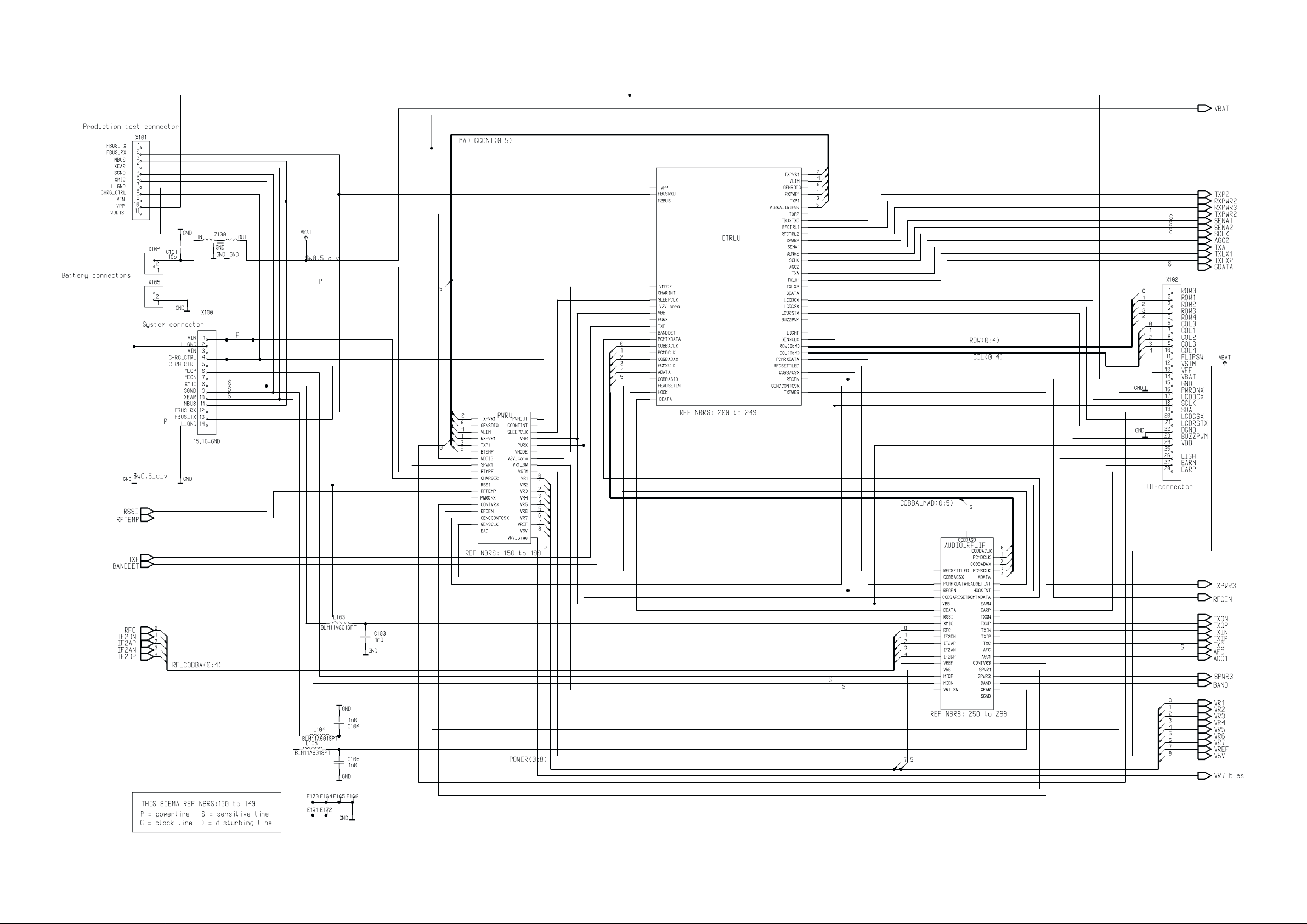
Circuit Diagram of System Blocks (Version 04.27 Edit 204)
System Module UT4S
NSW–1
Original 10/98 Updated 12/99
3/A3–1
Page 2
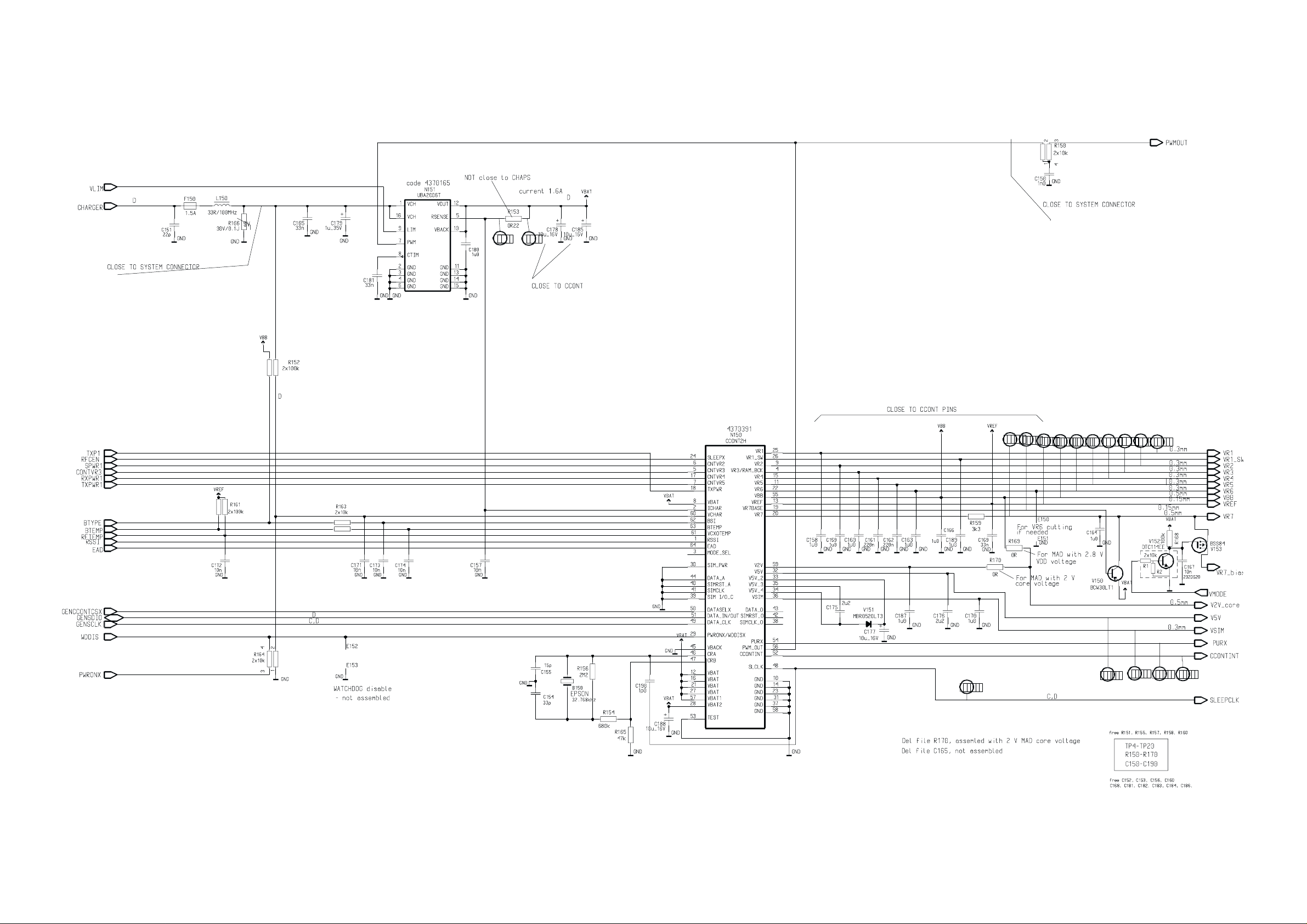
Circuit Diagram of Power Supply (Version 04.27 Edit 300)
TP4
TP5
System Module UT4S
NSW–1
TP20
TP11
TP12
TP13 TP8
TP15 TP6TP14
TP7
TP16
TP17
TP9
TP10
TP18
TP19
Original 10/98 Updated 12/99
3/A3–2
Page 3
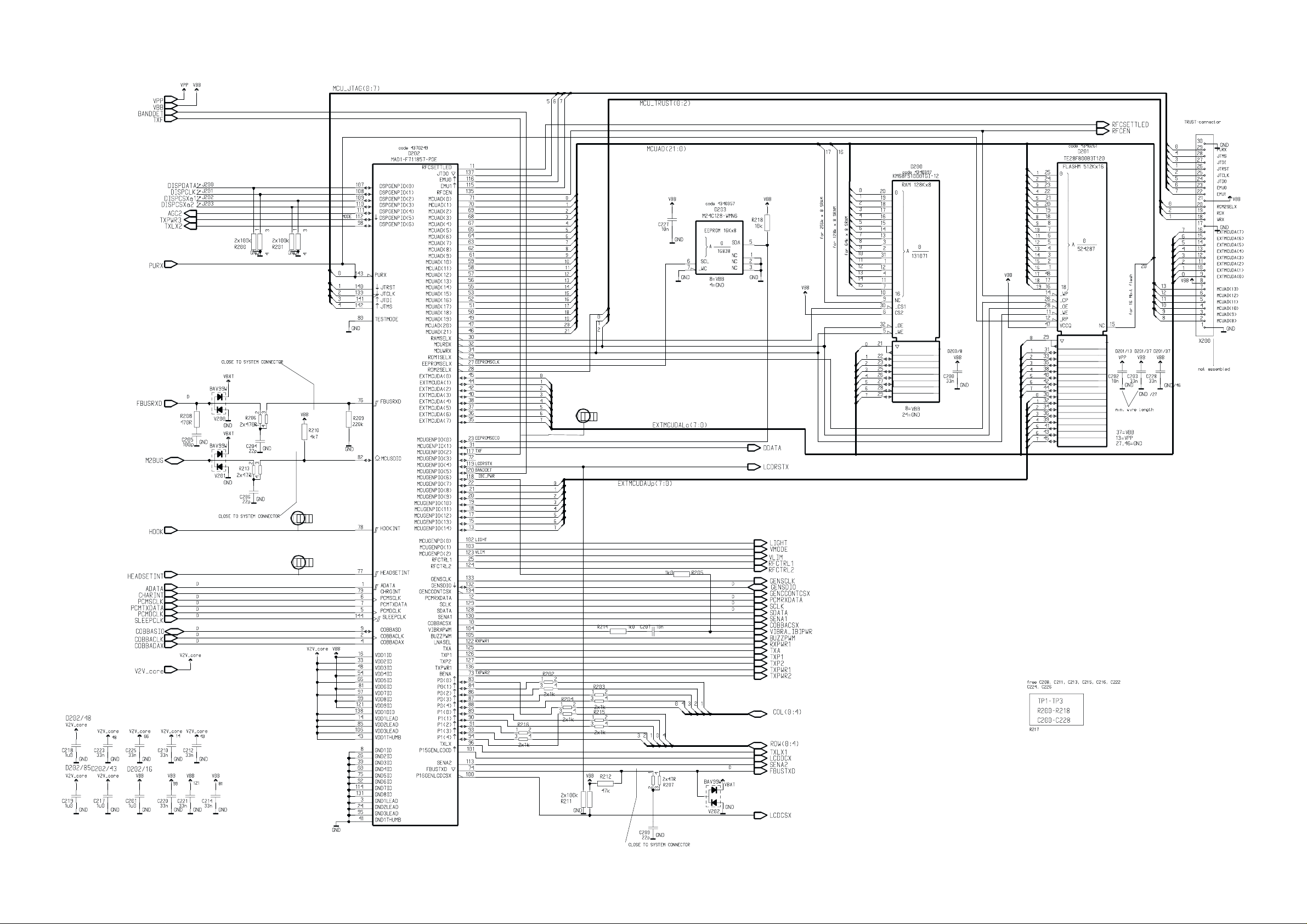
Circuit Diagram of CTRLU Block (Version 04.27 Edit 293)
System Module UT4S
NSW–1
TP1
TP2
TP3
Original 10/98 Updated 12/99
3/A3–3
Page 4
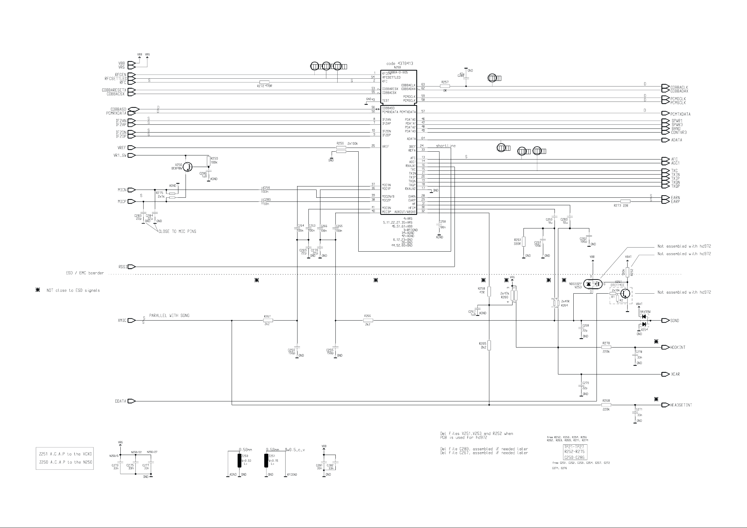
Circuit Diagram of Audio (Version 04.27 Edit 241)
TP21
TP22
TP23
System Module UT4S
TP24
NSW–1
TP25
TP26
TP27
Original 10/98 Updated 12/99
3/A3–4
Page 5
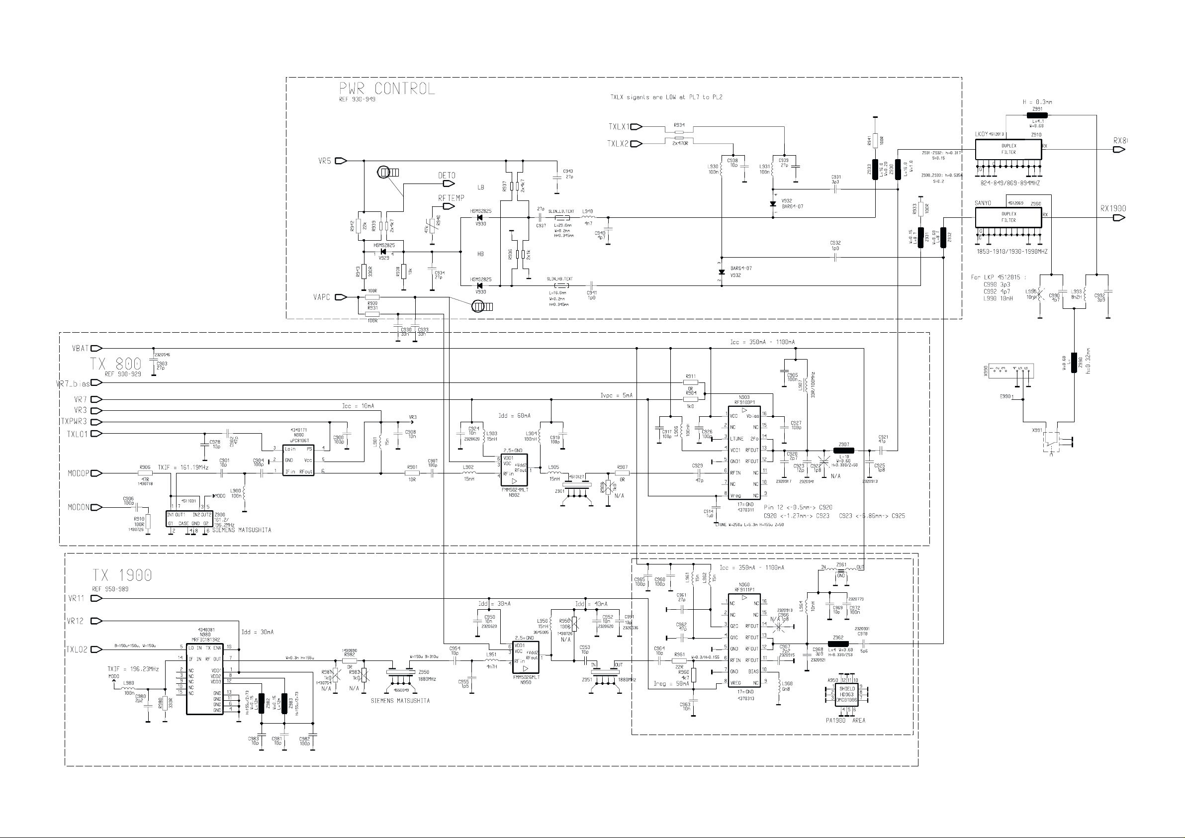
Circuit Diagram of Transmitter (Version 04.27 Edit 583)
TP33
TP34
System Module UT4S
NSW–1
Original 10/98 Updated 12/99
3/A3–5
Page 6
Circuit Diagram of Receiver (Version 04.27 Edit 131)
TP35
System Module UT4S
NSW–1
Original 10/98 Updated 12/99
3/A3–6
Page 7
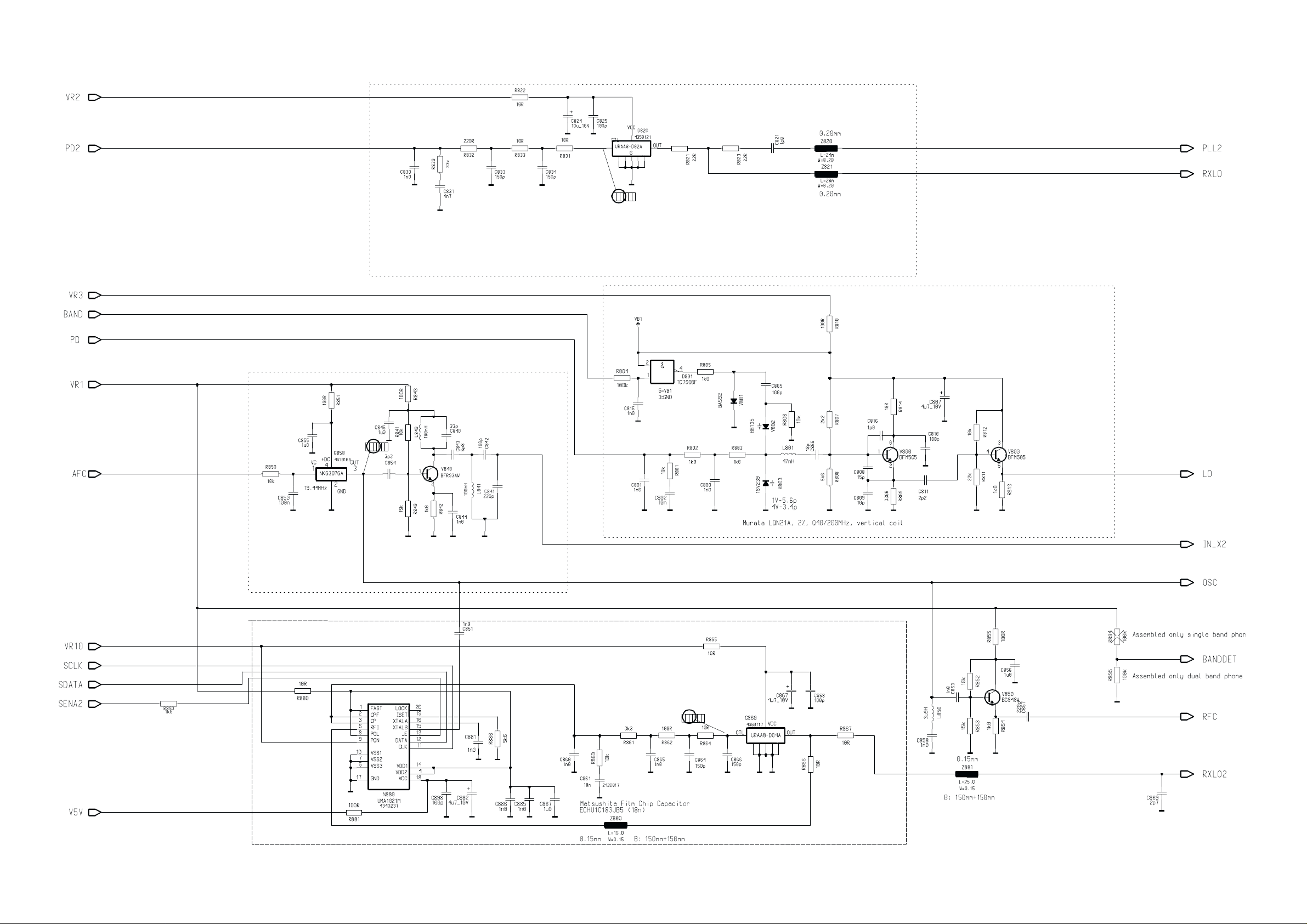
Circuit Diagram of Synthesizer (Version 04.27 Edit 157)
TP31
System Module UT4S
NSW–1
TP30
TP32
Original 10/98 Updated 12/99
3/A3–7
Page 8

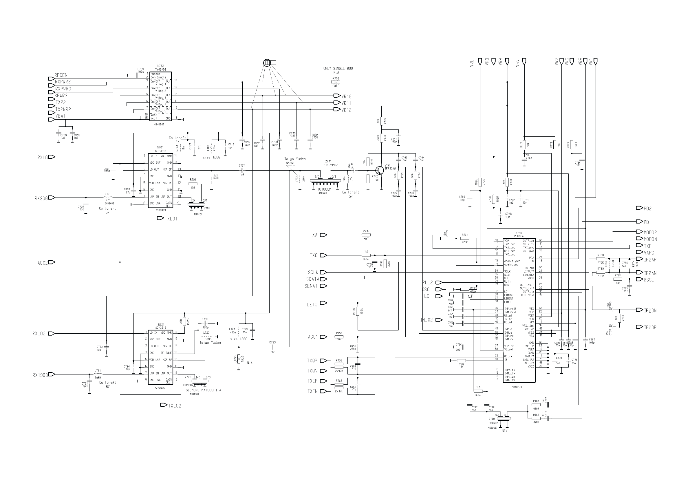
Circuit Diagram of RF Block (Version 04.27 Edit 105)
System Module UT4S
NSW–1
Original 10/98 Updated 12/99
3/A3–8
Page 9

Layout Diagram of UT4S
System Module UT4S
NSW–1
testpoint name condition dc–level ac–level
J200 Only for R&D use
J201 Only for R&D use
J202 Only for R&D use
J203 Only for R&D use
TP1, D202 pin 78 HOOKINT Remote controlheadset pulse active 2.8 V, non–active 0 V
TP2, D202 pin 77 HEADSETINT Headset connected pulse active 0 V, non–active 2.8 V
TP3, D202 pin 117 TXF False transmission indicator Irregular from 0 V to 2.8 V
TP4, R153 RSENSE VOUT detection min 0V, typ 3.6 V, max 5.2 V
TP5, R153 VOUT VOUT detection min 0V, typ 3.6 V, max 5.2 V
TP30, G850 pin 3 VCTCXO power on typ. 0.8 V – 1.2 Vpp sinewave 19.44 MHz
TP31, G820 pin 3 CTL active state ch 300 typ. 2.2 V
TP32, G860 pin 3 CTL active state ch 1000 typ. 2.2 V
Original 10/98 Updated 12/99
3/A3–9
Page 10

Layout Diagram of UT4S
System Module UT4S
NSW–1
testpoint name condition dc–level ac–level
TP6, N150 pin 11 VR5 supply for TX 2.8 V min 2.7 V / max 2.85 V
TP7, N150 pin 15 VR4 regulated supply for RX 2.8 V min 2.7 V / max 2.85 V
TP8, N150 pin 4 VR3 regulated supply for TX 2.8 V min 2.7 V / max 2.85 V
TP9, N150 pin 9 VR2 regulated supply for
SYNT
TP10, N150 pin 25 VR1 regulated supply for
VCTCXO
TP11, N150 pin 20 VR7 regulated supply for TX 2.8 V min 2.7 V / max 2.85 V
TP12, N150 pin 19 VR7BASEVR7 regulator external
transistor base current
TP13, N150 pin 13 VREF ref.voltage for N150 1.5 V +/– 1.5%
TP14, N150 pin 55 VBB regulated supply for
BaseBand
TP15, N150 pin 22 VR6 regulated supply for
COBBA
TP16, N150 pin 32 V5V regulated supply to
2GHz PLL
TP17, N150 pin 36 VSIM regulated supply for
flashing
TP18, N150 pin 54 PURX RESET Power up/down reset state 0 V, normal state 2.8
2.8 V min 2.7 V / max 2.85 V
2.8 V min 2.7 V / max 2.85 V
2.8 V min 2.7 V / max 2.85 V
2.8 V min 2.7 V / max 2.85 V
2.8 V min 2.7 V / max 2.85 V
5.0 V min 4.8 V / max 5.2 V
3.0 V min 2.8 V / max 3.2 V
V
testpoint name condition/type dc–level ac–level
TP19, N150 pin 52 CCON-
TINT
TP20, N150 pin 48 SLCLK 32.768 kHz, power on pulsed DC (0V/2.8 V)
TP21, N250 pin 1 RFCEN active state pulse active 2.8 V, non–active 0
TP22, N250 pin 54 RFCSE
TTLED
TP23, N250 pin 2 RFC 19.44 MHz sinewave 0.2Vpp–1V
TP24, N250 pin 63 COB-
BACLK
TP25, N250 pin 64 ADATA active state pulsed DC (0V/2.8V)
TP26, N250 pin 13 AFC Autom.Freq.control 0 – 2.3 V, typ. 1.15 V (room
TP27, N250 pin 15 TXC TX power control voltage @level 10 typ.ca 0.5 V pulse
TP33, R939 DETO active state 0.4 V – 2.2 V
TP34, R220 VAPC active state 0 V – 1.5 V typ.
TP35, N702 pins
9,11,12.13,14
VR8 –
VR 12
Charger interrupt pulse active 2.8 V, non–active 0
V
V
active state pulse active 2.8 V, non–active 0
V
pp sinewave
9.72 MHz, active state pulsed DC (0V/2.8V)
temp)
@level 2 typ.ca 1.7 V pulse
power on nominal 2.8 V
Original 10/98 Updated 12/99
[]
3/A3–10
Page 11

Circuit Diagram of System Blocks (Version 04.72 Edit 11)
System Module UT4S
NSW–1
Original 10/98 Updated 12/99
3/A3–11
Page 12

Circuit Diagram of Power Supply (Version 04.72 Edit 8)
System Module UT4S
TP4
TP5
NSW–1
TP20
TP11
TP12
TP13
TP14
TP15
TP8
TP6
TP16
TP9
TP17
TP10
TP18
TP19
TP7
Original 10/98 Updated 12/99
3/A3–12
Page 13

Circuit Diagram of CTRLU Block (Version 04.72 Edit 9)
System Module UT4S
NSW–1
TP3
TP1
TP2
Original 10/98 Updated 12/99
3/A3–13
Page 14

Circuit Diagram of Audio (Version 04.72 Edit 7)
TP21
TP22
TP23
System Module UT4S
TP24
NSW–1
TP25
TP26
TP27
Original 10/98 Updated 12/99
3/A3–14
Page 15

Circuit Diagram of Transmitter (Version 04.72 Edit 8)
TP33
TP34
System Module UT4S
NSW–1
Original 10/98 Updated 12/99
3/A3–15
Page 16

Circuit Diagram of Receiver (Version 04.72 Edit 8)
TP35
System Module UT4S
NSW–1
Original 10/98 Updated 12/99
3/A3–16
Page 17

Circuit Diagram of Synthesizer (Version 04.72 Edit 6)
TP31
System Module UT4S
NSW–1
TP30
TP32
Original 10/98 Updated 12/99
3/A3–17
Page 18

Circuit Diagram of RF Block (Version 04.72 Edit 5)
System Module UT4S
NSW–1
Original 10/98 Updated 12/99
3/A3–18
Page 19

Circuit Diagram of RF–BB Interface (Version 04.72 Edit 8)
System Module UT4S
NSW–1
Original 10/98 Updated 12/99
3/A3–19
Page 20

Layout Diagram of UT4S
System Module UT4S
NSW–1
testpoint name condition dc–level ac–level
J200 Only for R&D use
J201 Only for R&D use
J202 Only for R&D use
J203 Only for R&D use
TP1, D202 pin 78 HOOKINT Remote controlheadset pulse active 2.8 V, non–active 0 V
TP2, D202 pin 77 HEADSETINT Headset connected pulse active 0 V, non–active 2.8 V
TP3, D202 pin 117 TXF False transmission indicator Irregular from 0 V to 2.8 V
TP4, R153 RSENSE VOUT detection min 0V, typ 3.6 V, max 5.2 V
TP5, R153 VOUT VOUT detection min 0V, typ 3.6 V, max 5.2 V
TP30, G850 pin 3 VCTCXO power on typ. 0.8 V – 1.2 Vpp sinewave 19.44 MHz
TP31, G820 pin 3 CTL active state ch 300 typ. 2.2 V
TP32, G860 pin 3 CTL active state ch 1000 typ. 2.2 V
Original 10/98 Updated 12/99
3/A3–20
Page 21

Layout Diagram of UT4S
System Module UT4S
NSW–1
testpoint name condition dc–level ac–level
TP6, N150 pin 11 VR5 supply for TX 2.8 V min 2.7 V / max 2.85 V
TP7, N150 pin 15 VR4 regulated supply for RX 2.8 V min 2.7 V / max 2.85 V
TP8, N150 pin 4 VR3 regulated supply for TX 2.8 V min 2.7 V / max 2.85 V
TP9, N150 pin 9 VR2 regulated supply for
SYNT
TP10, N150 pin 25 VR1 regulated supply for
VCTCXO
TP11, N150 pin 20 VR7 regulated supply for TX 2.8 V min 2.7 V / max 2.85 V
TP12, N150 pin 19 VR7BASEVR7 regulator external
transistor base current
TP13, N150 pin 13 VREF ref.voltage for N150 1.5 V +/– 1.5%
TP14, N150 pin 55 VBB regulated supply for
BaseBand
TP15, N150 pin 22 VR6 regulated supply for
COBBA
TP16, N150 pin 32 V5V regulated supply to
2GHz PLL
TP17, N150 pin 36 VSIM regulated supply for
flashing
TP18, N150 pin 54 PURX RESET Power up/down reset state 0 V, normal state 2.8
2.8 V min 2.7 V / max 2.85 V
2.8 V min 2.7 V / max 2.85 V
2.8 V min 2.7 V / max 2.85 V
2.8 V min 2.7 V / max 2.85 V
2.8 V min 2.7 V / max 2.85 V
5.0 V min 4.8 V / max 5.2 V
3.0 V min 2.8 V / max 3.2 V
V
testpoint name condition/type dc–level ac–level
TP19, N150 pin 52 CCON-
TINT
TP20, N150 pin 48 SLCLK 32.768 kHz, power on pulsed DC (0V/2.8 V)
TP21, N250 pin 1 RFCEN active state pulse active 2.8 V, non–active 0
TP22, N250 pin 54 RFCSE
TTLED
TP23, N250 pin 2 RFC 19.44 MHz sinewave 0.2Vpp–1V
TP24, N250 pin 63 COB-
BACLK
TP25, N250 pin 64 ADATA active state pulsed DC (0V/2.8V)
TP26, N250 pin 13 AFC Autom.Freq.control 0 – 2.3 V, typ. 1.15 V (room
TP27, N250 pin 15 TXC TX power control voltage @level 10 typ.ca 0.5 V pulse
TP33, R939 DETO active state 0.4 V – 2.2 V
TP34, R220 VAPC active state 0 V – 1.5 V typ.
TP35, N702 pins
9,11,12.13,14
VR8 –
VR 12
Charger interrupt pulse active 2.8 V, non–active 0
V
V
active state pulse active 2.8 V, non–active 0
V
pp sinewave
9.72 MHz, active state pulsed DC (0V/2.8V)
temp)
@level 2 typ.ca 1.7 V pulse
power on nominal 2.8 V
Original 10/98 Updated 12/99
3/A3–21
 Loading...