

Page 1

Nokia Customer Care
NPL-4/5 Series Transceivers
System Module and User
Interface
Issue 1 05/04 Copyright © 2004 Nokia Corporation. All rights reserved.
Page 2

NPL-4/5
System Module and User Interface Nokia Customer Care
[This page left intentionally blank]
Page 2 Copyright © 2004 Nokia Corporation. All rights reserved. Issue 1 05/04
Page 3

NPL-4/5
Nokia Customer Care System Module and User Interface
Table of Contents
Page No
Glossary of Terms..................................................................................................................................... 7
Introduction ........................................................................................................................................... 10
Electrical modules ..............................................................................................................................10
Interconnection diagram ..................................................................................................................10
Temperature conditions ....................................................................................................................11
Humidity ...............................................................................................................................................11
System Module...................................................................................................................................... 12
Baseband module ...............................................................................................................................12
Technical summary ............................................................................................................................13
PWB .................................................................................................................................................... 15
DC characteristics ..............................................................................................................................15
External and internal signals and connections ..........................................................................18
UI board interface signals ................................................................................................................24
Display interface signals............................................................................................................... 25
System connector interface signals ..............................................................................................26
SIM interface signals .........................................................................................................................27
FCI interface signals ..........................................................................................................................28
Camera interface signals ..................................................................................................................28
FM radio interface signals ...............................................................................................................29
Compass interface signals ...............................................................................................................30
Functional Description ........................................................................................................................ 31
Modes of operation ............................................................................................................................31
No supply ..............................................................................................................................................31
Backup ...................................................................................................................................................31
Acting dead ..........................................................................................................................................31
Active .....................................................................................................................................................31
Sleep mode ...........................................................................................................................................32
Charging ................................................................................................................................................33
Power up and reset ............................................................................................................................33
Power up with PWR key ...................................................................................................................34
Power up when charger is connected ..........................................................................................34
Battery ...................................................................................................................................................34
A/D channels ........................................................................................................................................36
Digital camera .....................................................................................................................................36
FM radio ................................................................................................................................................37
Electrical compass ..............................................................................................................................38
Thermometer ........................................................................................................................................38
Backup battery ....................................................................................................................................39
SIM interface .......................................................................................................................................39
FCI (Functional Cover Interface) ...................................................................................................40
Memory .................................................................................................................................................41
External memory .................................................................................................................................42
Compass .................................................................................................................................................. 43
Earth magnetic field ..........................................................................................................................43
Heading angle or azimuth (a) .................................................................................................... 44
Inclination (d) .................................................................................................................................. 44
Declination (l) .................................................................................................................................. 44
Issue 1 05/04 Copyright © 2004 Nokia Corporation. All rights reserved. Page 3
Page 4

NPL-4/5
System Module and User Interface Nokia Customer Care
Tilt (s).................................................................................................................................................. 45
HW Block Diagram ............................................................................................................................... 46
HW block functions ...........................................................................................................................46
Magnetometer Sensor......................................................................................................................... 48
Main features ......................................................................................................................................48
Block diagram ......................................................................................................................................49
Magnetometer control interface ...................................................................................................49
Pin Assignment................................................................................................................................ 49
Test Circuitry.......................................................................................................................................... 51
MagIC ASIC....................................................................................................................................... 51
Main features ......................................................................................................................................52
Block diagram and functional descriptions ................................................................................52
MagIC control interface ...................................................................................................................53
Pin assignment ................................................................................................................................ 53
MagIC ASIC interface - Magnetometer sensor...................................................................... 53
MagIC ASIC – UPP interface........................................................................................................ 54
MagIC ASIC – UEME interface.................................................................................................... 55
MagIC ASIC – UPP - External power supply interface......................................................... 55
MagIC - magnetometer sensor interface for constant current driver............................. 56
Power supplies .....................................................................................................................................56
Introduction...................................................................................................................................... 56
Using VIO for DVDD supply.......................................................................................................... 56
Using external regulator for AVDD............................................................................................ 56
Compass and phone basics ..............................................................................................................57
Phone directions .................................................................................................................................57
General description ............................................................................................................................58
Operation modes............................................................................................................................. 58
Compass function main features ...................................................................................................58
Compass display menu.................................................................................................................. 58
Compass display results................................................................................................................ 58
Compass calibration SW ........................................................................................................
User assisted calibration............................................................................................................... 59
Compass declination menu ..............................................................................................................59
Testpoints................................................................................................................................................ 60
Set/Reset ...............................................................................................................................................60
VBRIDGE ................................................................................................................................................60
Channel output A ...............................................................................................................................60
Channel output B ...............................................................................................................................60
Service Software Interface (Phoenix) ............................................................................................. 61
Performance........................................................................................................................................... 62
Calibration basics ...............................................................................................................................62
Calibration process flow ...................................................................................................................63
Compass digital values, limit values .............................................................................................63
Clock distribution ...............................................................................................................................65
User Interface ........................................................................................................................................ 66
Display .......................................................................................................................
UI Board ................................................................................................................................................67
Power supply for LEDs .......................................................................................................................68
............................66
...........59
Page 4 Copyright © 2004 Nokia Corporation. All rights reserved. Issue 1 05/04
Page 5

NPL-4/5
Nokia Customer Care System Module and User Interface
Keyboard LEDs driver .........................................................................................................................68
Display and air bubble LED driver ..................................................................................................69
Flashlight LEDs driver ........................................................................................................................69
Internal microphone ..........................................................................................................................70
Internal speaker ..................................................................................................................................71
IHF ...........................................................................................................................................................71
Headset connections .........................................................................................................................72
Vibra .......................................................................................................................................................73
RF Module............................................................................................................................................... 74
RF frequency plan........................................................................................................................... 75
DC characteristics ..............................................................................................................................76
Regulators......................................................................................................................................... 76
Power distribution.......................................................................................................................... 77
RF characteristics ...............................................................................................................................78
RF block diagram ............................................................................................................................ 79
RF block diagram NPL-4/5 ........................................................................................................... 79
Frequency synthesizers ................................................................................................................. 80
Receiver ............................................................................................................................................. 80
Transmitter ....................................................................................................................................... 81
Antenna switch module................................................................................................................ 82
Power Amplifier............................................................................................................................... 83
RF ASIC Helgo.................................................................................................................................. 84
AFC function .................................................................................................................................... 84
Antenna............................................................................................................................................ 84
List of Figures
Page No
Fig 1 Interconnection diagram................................................................................................................... 10
Fig 2 Baseband blocks. ................................................................................................................................ 13
Fig 3 PWB vias ................................................................................................................................................ 15
Fig 4 Power Distribution Diagram............................................................................................................. 18
Fig 5 Battery Pack Contacts........................................................................................................................ 35
Fig 6 Camera Connections to Baseband.................................................................................................. 37
Fig 7 FM Radio Audio-, Antenna- and Digital Interface Connections............................................ 37
Fig 8 Baseband and Compass Interface................................................................................................... 38
Fig 9 Ambient Temperature Sensor Interface to BB ............................................................................ 39
Fig 10 UPP/UEMEK SIM Interface Connections ....................................................................................40
Fig 11 FCI Interface....................................................................................................................................... 41
Fig 12 FCI Connector Pin Order on PWB................................................................................................. 41
Fig 13 Earth’s Magnetic Field..................................................................................................................... 44
Fig 14 Earths’s Magnetic Field Components.......................................................................................... 45
Fig 15 Block Diagram.................................................................................................................................... 46
Fig 16 Magnetometer Sensor Block Diagram ........................................................................................ 49
Fig 17 Pin Assignment In Package............................................................................................................ 50
Fig 18 Test Circuitry ...................................................................................................................................... 51
Fig 19 Offset strap coil current effect ......................................................................................
Fig 20 Block Diagram.................................................................................................................................... 52
Fig 21 Directions Through Phone .............................................................................................................. 57
............... 51
Issue 1 05/04 Copyright © 2004 Nokia Corporation. All rights reserved. Page 5
Page 6

NPL-4/5
System Module and User Interface Nokia Customer Care
Fig 22 Timing and Voltage Level l ............................................................................................................. 60
Fig 23 What Happened on Calibration (Track on x/y Plane while rotating) ................................. 63
Fig 24 Clock Distribution Diagram............................................................................................................ 65
Fig 25 User Interface Connections............................................................................................................ 66
Fig 26 Display Block ...................................................................................................................................... 66
Fig 27 UI Board............................................................................................................................................... 67
Fig 28 VLED Voltage Supply........................................................................................................................ 68
Fig 29 Keyboard Led Driver and Control Diagram ................................................................................69
Fig 30 Display and Air Bubble LEDs driver and Control Diagram..................................................... 69
Fig 31 Flashlight Driver and Control ........................................................................................................ 70
Fig 32 Microphone Connection.................................................................................................................. 70
Fig 33 IEarpiece Connection....................................................................................................................... 71
Fig 34 IHF Connection.................................................................................................................................. 71
Fig 35 NPL-4/5 Audio Connections .......................................................................................................... 73
Fig 36 RF Frequency plan............................................................................................................................. 75
Fig 37 Power distribution diagram ......................................................................................................... 77
Fig 38 RF Block Diagram.............................................................................................................................. 79
Fig 39 Antenna Switch Module ................................................................................................................ 83
Fig 40 Power Amplifier ................................................................................................................................ 84
Page 6 Copyright © 2004 Nokia Corporation. All rights reserved. Issue 1 05/04
Page 7

NPL-4/5
Nokia Customer Care System Module and User Interface
Glossary of Terms
ACI Accessory Control Interface
ADC Analog-Digital Converter
AEC Acoustic Echo Canceller
AFC Automatic Frequency Control
AGC Automatic Gain Control
AIF Application Interface
API Application Programming Interface
ARM Processor architecture
ASIC Application Specific Integrated Circuit
BB Baseband
CCI Camera Control Interface
CCP Compact Camera Port
CMT Cellular Mobile Telephone (MCU and DSP)
CPU Central Processing Unit
CTSI Clocking Timing Sleep Interrupt
CSP Chip Scale Package
DAC Digital-Analog Converter
DAI Digital Audio Interface
DB Dual band
DCT3 Digital Core Technology, 3rd generation
DCN Offset Cancellation control signal
DLL Dynamic Link Library
DRC Dynamic Range Controller
DSP Digital Signal Processor
Issue 1 05/04 Copyright © 2004 Nokia Corporation. All rights reserved. Page 7
Page 8

NPL-4/5
System Module and User Interface Nokia Customer Care
EGSM Extended – GSM
EFR Enhanced Full Rate
EGPRS Enhanced General Packet Radio Service
EMC Electromagnetic compatibility
EMI Electromagnetic Interference
EXT RF External RF
FBUS Asynchronous Full Duplex Serial Bus
GPRS General Packet Radio Service
GSM Global System for Mobile communications
HS Half Rate Speech
HSCSD High Speed Circuit Switched Data
IC Integrated Circuit
I/O Input/Output
IrDA Infrared Association
LCD Liquid Crystal Display
LNA Low Noise Amplifier
MBUS 1-wire half duplex serial bus
MCU Micro Controller Unit
MDI MCU-DSP Interface
MFI Modulator and Filter Interface
PA Transmit Power Amplifier
PC Personal Computer
PCM Pulse Code Modulation
PCM SIO Synchronous serial bus for PCM audio transferring
Page 8 Copyright © 2004 Nokia Corporation. All rights reserved. Issue 1 05/04
Page 9

NPL-4/5
Nokia Customer Care System Module and User Interface
PCMCIA PC Memory Card International Association
PIFA Planar Inverted F-antenna
PWB Printed Wiring Board
RF Radio Frequency
SIM Subscriber Identity Module
UEMEK Enhanced Universal Energy Management
UI User Interface
UPP Universal Phone Processor
VCXO Voltage Controlled Crystal Oscillator
VCTCXO Voltage Controlled Temperature Compensated Crystal Oscillator.
Issue 1 05/04 Copyright © 2004 Nokia Corporation. All rights reserved. Page 9
Page 10
NPL-4/5
T
System Module and User Interface Nokia Customer Care
Introduction
Electrical modules
The system module consists of Radio Frequency (RF) and baseband (BB). User Interface
(UI) contains display, keyboard, IR link, vibra, HF/HS connector and audio parts.
FM radio is located on the main PWB.
The electrical part of the keyboard is located in separate UI PWB. It is connected to radio
PWB through spring connectors.
The Baseband blocks provide the MCU, DSP, external memory interface and digital control functions in the UPP ASIC. Power supply circuitry, charging, audio processing and RF
control hard ware are in the UEMEK ASIC.
The purpose of the RF block is to receive and demodulate the radio frequency signal from
the base station and to transmit a modulated RF signal to the base station.
The UI module is described in a dedicated section of the manual.
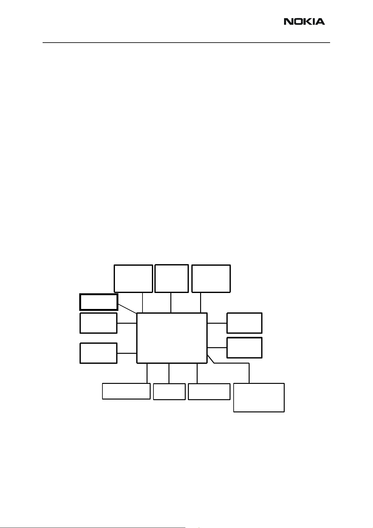
Interconnection diagram
Keyboard
module
Flashlight
Antenna
Microphone
Figure 1: Interconnection diagram
Display
IHF
speaker
Radio
Module
NPL-4/5
NHL-4
IR Link
Earpiece
BatterySIM
Charger
omahawk
Accessories
Page 10 Copyright © 2004 Nokia Corporation. All rights reserved. Issue 1 05/04
Page 11

NPL-4/5
Nokia Customer Care System Module and User Interface
Temperature conditions
Specifications are met within range of -10...+55 deg. C ambient temperature
Storage temperature range -40...+70 deg. C
Humidity
Relative humidity range is 5... 95%.
This module is not protected against water. Condensated or splashed water might cause
malfunction momentary. Long term wetness will cause permanent damage.
Issue 1 05/04 Copyright © 2004 Nokia Corporation. All rights reserved. Page 11
Page 12

NPL-4/5
System Module and User Interface Nokia Customer Care
System Module
The System module (or Engine) consists of Baseband and RF sub-modules, each described
below.
Baseband module
Product NPL-4/5 is a DCT4 Active segment phone. There are two variants: An EGSM900 /
GSM1800 / GSM1900 phone and a US variant with GSM850/1800/1900.
The HW has the following features:
• HSCSD, GPRS (MSC10) and EGPRS (MSC6)
• DCT4 engine with UPP8M v3.5 and UEMEk v1.1
• AMR and 16 MIDI tones
• 128/16 Mbit Psram Combo memory
• Passive display with 4k colours
• Battery BL-5B
• Pop-Port interface
• 5-way navigation key with select
• Electrical compass
• FCI on bottom cover
• VGA Camera
•Vibra
•IHF
•FM Radio
•IrDA
•Torch
• PTT key
•Sidekeys
The NPL-4/5 BB is based on the DCT4 engine and is compatible to the Pop-Port accessories. The DCT4/4.5 engine consists basically of two ASICs. The UEMEK (Enhanced Universal Energy Management) IC including voltage regulators, charge control and audio
circuits, audio IFH amplifier from DCT4.5) and the UPP (Universal Phone Processor
including MCU, DSP and RAM from DCT4).
Page 12 Copyright © 2004 Nokia Corporation. All rights reserved. Issue 1 05/04
Page 13
NPL-4/5
j
A
Nokia Customer Care System Module and User Interface
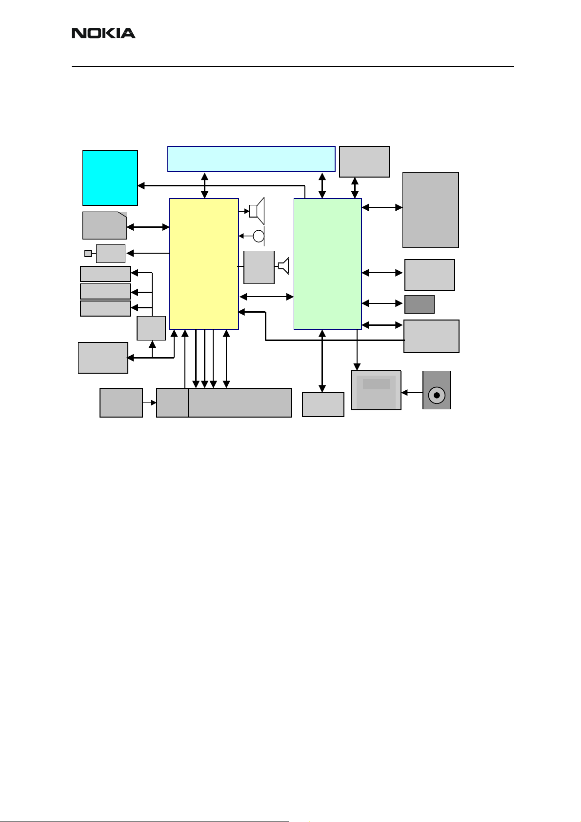
Technical summary
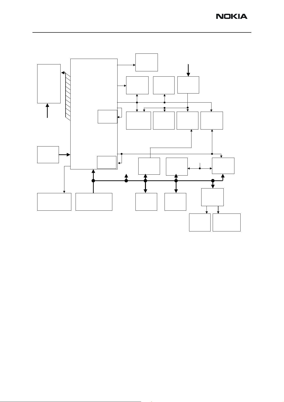
The picture below shows the main Baseband function blocks
Figure 2: Baseband blocks.
LCD
Passive colour
STN
SIM
RF Interface
Compass
PSRAM
COMBO
128Mbit
Flash
16Mbit
PSRAM
Vibra
Keyboard
Illumination
Display
Illumination
Flashlight
UEMEk
D-class
mplifier
IHF
UPP8M
v3
Keyboard
1.8 V
IR
DC/
FM radio
TEA5767
VGA VV6450
BATTERY BL-5B
Charge
DC
DC
ack
System connector
Tomahaw
FCI
HWA
STV0900
Baseband is running from power rails 2.8V analog voltage and 1.8V I/O voltage. UPP core
voltages can be lowered down to 1.0V, 1.3V and 1.5V. UEMEK includes 7 linear LDO (Low
Drop-Out) regulator for baseband and 7 regulators for RF. It also includes 4 current
sources for biasing purposes and internal usage. UEMEK also includes SIM interface
which has supports both 1.8V and 3V SIM cards. Note: 5V SIM cards are no longer sup-
ported by DCT-4 generation baseband.
A real time clock function is integrated into the UEMEK, which utilizes the same 32kHz
clock supply as the sleep clock. A backup power supply is provided for the RTC-battery,
which keeps the real time clock running when the main battery is removed. The backup
power supply is a rechargeable surface mounted Li-Ion battery. The backup time with the
battery is 30 minutes minimum.
A UEMEK ASIC handles the analog interface between the baseband and the RF section.
UEMEK provides A/D and D/A conversion of the in-phase and quadrature receive and
transmit signal paths and also A/D and D/A conversions of received and transmitted
audio signals to and from the user interface.
The UEMEK supplies the analog TXC and AFC signals to RF section according to the UPP
DSP digital control. Data transmission between the UEMEK and the UPP is implemented
using two serial busses, DBUS for DSP and CBUS for MCU. There are also separate signals
for PDM coded audio. Digital speech processing is handled by the DSP inside UPP ASIC.
Issue 1 05/04 Copyright © 2004 Nokia Corporation. All rights reserved. Page 13
Page 14

NPL-4/5
System Module and User Interface Nokia Customer Care
UEMEK is a dual voltage circuit, the digital parts are running from the baseband supply
1.8V and the analog parts are running from the analog supply 2.78V.
VBAT is directly used for Vibra, LED-driver, Audio amplifier and FCI (Functional Cover
Interface).
The baseband architecture supports a power saving function called ”sleep mode”. This
sleep mode shuts off the VCTCXO, which is used as system clock source for both RF and
baseband. During the sleep mode the system runs from a 32 kHz crystal. The phone is
waken up by a timer running from this 32 kHz clock supply. The sleep time is determined
by network parameters. Sleep mode is entered when both the MCU and the DSP are in
standby mode and the normal VCTCXO clock is switched off.
The baseband supports both internal and external microphone inputs and speaker outputs. UEMEK also includes third microphone input. This input is used for FM-radio. Input
and output signal source selection and gain control is done by the UEMEK according to
control messages from the UPP. Keypad tones, DTMF, and other audio tones are generated and encoded by the UPP and transmitted to the UEMEK for decoding. An external
vibra alert control signals are generated by the UEMEK with separate PWM outputs.
The NPL-4/5 uses D-class amplifier to amplifying IHF speaker audios. It gives more sound
pressure from speaker and efficiency is in good level to improve thermal performance
compared to AB-class.
VGA Camera is connected to baseband (UPP) through HW accelerator IC. The camera
data bus is common with display bus. The HWA is taking care of camera control and it is
compressing the pictures.
NPL-4/5 has 2-axes electrical compass. It is implemented with magnetoresistive sensor
and MagIC ASIC.
NPL-4/5 has two serial control interfaces: FBUS and MBUS. FBUS and MBUS can be
accessed through production test pattern and FBUS can be also accessed thought Tomahawk System Connector.
The FCI interface is located to front bottom side area of the phone. This means that only
B-cover can be an active cover.
EMC shielding is implemented using a metal body profile, RF cans and PWB grounding.
Some components are outside of shielding. Heat generated by the circuitry is conducted
out via the PWB ground planes and by using buried vias between PWB layers.
Page 14 Copyright © 2004 Nokia Corporation. All rights reserved. Issue 1 05/04
Page 15
NPL-4/5
V
y
Nokia Customer Care System Module and User Interface
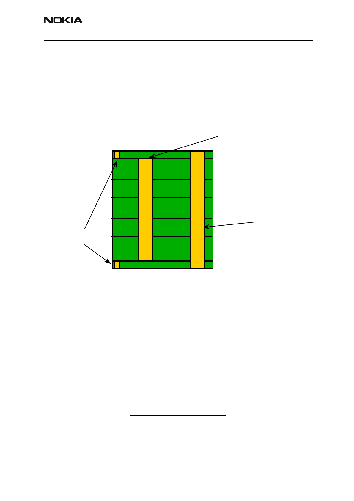
PWB
Characteristics of the PWB
8 layer board
Double side assembled
Figure 3: PWB vias
Buried via through
internal layers
TOP
RCC
Blind vias
BOTTOM
DC characteristics
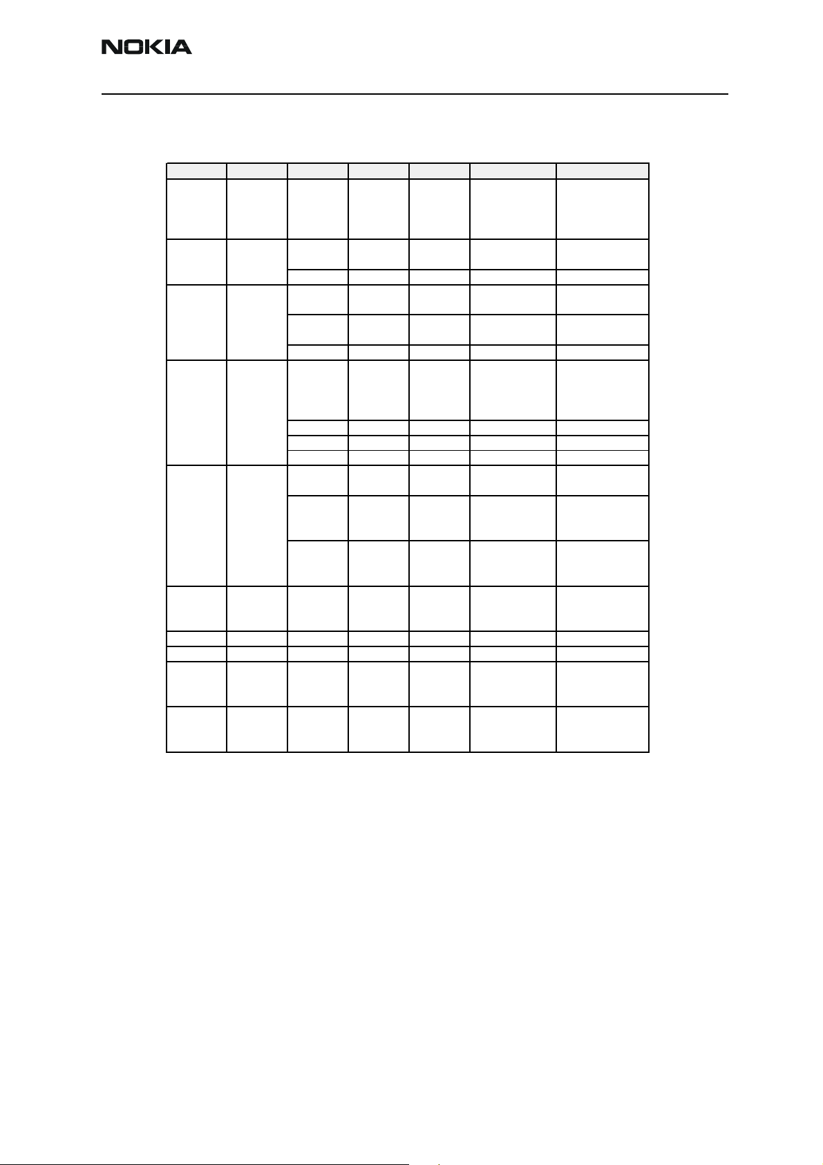
RCC
Table 1: Battery voltage range
Signal
Battery Voltage
(Idle)
Note
-0.3…5.5V
ia through all
ers
la
Battery Voltage
(Call)
Charger Input
Voltage
Max 4.8V
-0.3V …16V
Issue 1 05/04 Copyright © 2004 Nokia Corporation. All rights reserved. Page 15
Page 16
NPL-4/5
System Module and User Interface Nokia Customer Care
Table 2: UEMEK Regulators
Name Voltage (V) Current (mA)
Min Nom Max Max Sleep Max
VANA 2.7 2.78 2.86 80
VFLASH1 2.61 2.78 2.95 70 1.5
VIO 1.72 1.8 1.88 150 0.5
VCORE 1.48 1.57 1.66 200 0.2
VAUX1 50 0.5
VAUX2 2.7 2.78 2.86 70 0.5
VAUX3 2.7 2.78 2.86 10 0.5
VSIM 25 0.5
VR1A/B 4.6 4.75 4.9 10 VR2 100 -
VR3 2.7 2.78 2.86 20 VR4 2.7 2.78 2.86 50 0.1
VR5 2.7 2.78 2.86 50 0.1
VR6 2.7 2.78 2.86 50 0.1
VR7 2.7 2.78 2.86 45 -
1.745 1.8 1.855
2.91 3 3.09
1.745 1.8 1.855
2.91 3 3.09
2.7 2.78 2.86
-2.61 -2.78 -2.95
Page 16 Copyright © 2004 Nokia Corporation. All rights reserved. Issue 1 05/04
Page 17
NPL-4/5
Nokia Customer Care System Module and User Interface
Table 3: 1-3 External Regulators
Signal
name
VCAMDIG 1.755 1.8 1.845 0.0015 150 Power
VANA_EXT 2.72 2.8 2.88 0.0015 150 Power
Min Nom Max Sleep Iq Max
Voltage (V) Current (mA) Note
supply for
camera
digital
parts. Imax
= 150mA.
Cam and
HWA max
current
60mA
supply for
camera,
compass
and FMradio
analog
parts. Imax
= 150mA.
Issue 1 05/04 Copyright © 2004 Nokia Corporation. All rights reserved. Page 17
Page 18
NPL-4/5
V
V
V
V
V
V
V
V
V
V
V
V
System Module and User Interface Nokia Customer Care
Figure 4: Power Distribution Diagram
RF
BATRF
Charger
POPPORT
Tomahawk /
Vout
VR1A
VR1B
VR2
VR3
VR4
VR5
VR6
VR7
IPA1
IPA2
IPA3
UEMEk
AUX2
BL-5B Battery
SIM
CORE
IO
ANA
UEME
analog
parts
AUX1
AUX3
FLASH1
UEME
digital parts
COMPASS
BATRF
UPP
v3.5
SIM
Ext. 1.8V
regulator
IHF PA
D-class
COMBO
128/16M
FMRadio
VIBRA
Ext. 2.8V
regulator
HWA and
Camera
FCI
Interfac
BAT
LCD
CSTN
IO
IR
module
DC/DC
External and internal signals and connections
This section describes the external and internal electrical connection and interface levels
on the baseband. The electrical interface specifications are collected into tables that
covers a connector or a defined interface.
Flashlight
Disp and
keypad
Illumination
Page 18 Copyright © 2004 Nokia Corporation. All rights reserved. Issue 1 05/04
Page 19
NPL-4/5
Nokia Customer Care System Module and User Interface
Table 4: AC and DC Characteristics of DCT4 RF-Baseband Voltage Supplies
Signal
name
VBAT Battery PA &
VR1A Voltage 4.6 4.75 4.9 V
VR1B Current 2 10 MA
VR2 UEMEK HELGO85 Supply for
VR3 UEMEK VCTCXO,
VR4 UEMEK HELGO85 Supply for
VR5 UEMEK HELGO85 Supply for
From To Parameter Min Typ Max Unit Function
Voltage 2.95 3.6 4.2 V
UEMEK
Current 2000 MA
Current
drawn by
PA when
”off”
UEMEK HELGO85 Supply for
Noise
density
Voltage 2.7 2.78 2.86 V
Current 65 100 MA
Noise
density
f=100Hz 120 nVrms/
f>300Hz
Voltage 2.7 2.78 2.86 V
HELGO85
Current 1 20 MA
Noise
density
Voltage 2.7 2.78 2.86 V
Current 50 MA
Noise
density
f=6Hz 5500 nVrms/
f=60Hz 550
f>600Hz 55
Voltage 2.7 2.78 2.86 V
Current 50 MA
Noise
density
BW=100Hz.
.. 100kHZ
0.8 2
240 nVrms/
240 nVrms/
240 nVrms/
µA
sqrt(Hz)
sqrt(Hz)
sqrt(Hz)
sqrt(Hz)
sqrt(Hz)
Battery
supply. Cutoff level of
DCT4
regulators
is 3.2V.
Losses in
PWB tracks
and ferrites
are taken
account to
minimum
battery
voltage
level.
charge
pump for
SHF VCO
tuning.
I/Qmodulators,
buffers, ALS
Supply for
VCTCXO,
PLL digital
parts
HELGO85R
X; PA bias
blocks.
Noise
density
decades
20dB/deg
from 6Hz to
600 Hz.
From
f>600Hz
max. noise
density
nVrms/
sqrt(Hz)
HELGO85PL
L; dividers,
LO- buffers,
prescaler,
Issue 1 05/04 Copyright © 2004 Nokia Corporation. All rights reserved. Page 19
Page 20
NPL-4/5
µ
V
System Module and User Interface Nokia Customer Care
Table 5: AC and DC Characteristics of DCT4 RF-Baseband Voltage Supplies
VR6 UEMEK HELGO85 Supply for
VR7 UEMEK SHF VCO Supply for
VrefRF01 UEMEK HELGO85
VrefRF02 UEMEK VB_EXT Voltage 1.334 1.35 1.366
Voltage 2.7 2.78 2.86 V
Current 50 MA
Noise
density
BW=100Hz.
.. 100kHz
Voltage 2.7 2.78 2.86 V
Current 30 MA
Noise
density
100Hz<f<2
kHz
2kHz<f<10
kHz
10kHz<f<3
0kHz
30kHz<f<9
0kHz
90kHz<f<3
MHz
Voltage 1.334 1.35 1.366 V Voltage
Current 100
Temp Coef -65 65
Noise
density
BW=600Hz.
.. 100kHz
240 nVrms/
sqrt(Hz)
70 nVrms/
sqrt(Hz)
55
35
30
30
µA
/C
60 nVrms/
sqrt(Hz)
HELGO85
BB and
LNAs
SHF VCO
Reference
for
HELGO85
DCN2
op.amps.
Note
:
Below
600Hz
noise
density is
allowed to
increase 20
dB/oct
Note
V
Voltage
reference
for
HELGO85
bias block.
Not used
for
HELGO85
Page 20 Copyright © 2004 Nokia Corporation. All rights reserved. Issue 1 05/04
Page 21
NPL-4/5
T
µ
Nokia Customer Care System Module and User Interface
Table 6: AC and DC Characteristics of DCT4 RF-Baseband Digital Signals
Signal
name
TXP ”1” 1.38 1.88 V
(RFGenOut3
)
TXA UPP HELGO85 Power
RFBusEna1XUPP HELGO85 RFbus
From To Parameter Input Characteristics
Min
UPP HELGO85 Power
”0” 0 0.4 V
Load
Resistance
Load
Capacitanc
e
Timing
Accuracy
”1” 1.38 1.88 V
”0” 0 0.4 V
Load
Resistance
Load
Capacitanc
e
Timing
Accuracy
”1” 1.38 1.88 V
”0” 0 0.4 V
Current 50
Load
resistance
Load
capacitance
yp Max Unit
10 220
20 pF
¼ Symbol
10 220
20 pF
¼ symbol
10 220
20 pF
k
k
kΩ
Ω
Ω
A
Function
amplifier
enable
control loop
enable
enable
RFBusData UPP HELGO85 RFbus
RFBusClk UPP HELGO85 RFBus clock
RESET ”1” 1.38 1.85 V
(GENIO06) ”0” 0 0.4 V
UPP HELGO85 Reset to
”1” 1.38 1.88 V
”0” 0 0.4 V
Load
resistance
Load
capacitance
Data
frequency
”1” 1.38 1.88 V
”0” 0 0.4 V
Load
resistance
Load
capacitance
Data
frequency
Load
capacitance
Load
resistance
Timing
accuracy
10 220
20 pF
10 MHz
10 220
20 pF
10 MHz
20 pF
10 220
¼ symbol
data;
k
Ω
k
Ω
k
Ω
read/write
HELGO85
Issue 1 05/04 Copyright © 2004 Nokia Corporation. All rights reserved. Page 21
Page 22
NPL-4/5
System Module and User Interface Nokia Customer Care
Table 7: AC and DC Characteristics of DCT4 RF-Baseband Analogue Signals
Signal
name
VCTCXO VCTCXO UPP High
VCTCXOGnd VCTCXO UPP DC Level 0 V Ground for
RXI/RXQ HELGO85 UEMEK Received
TXIP / TXIN UEMEK HELGO88
TXQP /
TXQN
AFC UEMEK VCTCXO
From To Parameter Min Typ Max Unit Function
Frequency 13 26 MHz
stability
clock signal
for the
logic
circuits, AC
coupled.
Distorted
sinewave
e.g.
sawtooth.
reference
clock
demodulate
d IQ signals
ble voltage
swing.
ble
common
mode
voltage.
Between
TXIP-TXIN
frequency
control
signal for
VCTCXO
UEMEK HELGO85
Signal
amplitude
Input
Impedance
Input
Capacitanc
e
Harmonic
Content
Clear signal
window (no
glitch)
Duty Cycle 40 60 %
Voltage
swing
(static)
DC level 1.3 1.35 1.4 V
I/Q
amplitude
mismatch
I/Q phase
mismatch
Differential
voltage
swing
(static)
DC level 1.17 1.2 1.23 V Programma
Source
Impedance
Same spec as for TXIP / TXIN
Voltage
Min
Max
Resolution 11 Bits
Load
resistance
and
capacitance
0.2 0.8 2 Vpp
10
300 mVpp
1.35 1.4 1.45 Vpp
-5 5 Deg
2.15 2.2 2.25 Vpp Programma
00.1
2.4 2.6
1
K
Ω
10 pF
-8 dBc
0.2 DB
200
Ω
V Automatic
k
Ω
100 nF
Source
Impedance
200
Ω
Page 22 Copyright © 2004 Nokia Corporation. All rights reserved. Issue 1 05/04
Page 23
NPL-4/5
Nokia Customer Care System Module and User Interface
TxC UEMEK HELGO85
RFTemp HELGO85 UEMEK Temperatur
DC_sense PA UEMEK Voltage 0.6 V PA final
IPA1 / IPA2 UEMEK PA PA final
VCTCXOTEMPPA sheet UEMEK A/D Voltage
Voltage
Min
Max
Source
Impedance
Resolution 10 Bits
Voltage at 20oC
Voltage at
+25oC
Voltage at
+60oC
Output
Voltage
Current
range
Resolution 4 Bits
Current
tolerance
Noise
density
f=100 Hz-
800kHz
f=800kHz-
100MHz
2.4
1,57 V
1,7
1,79
02.7V
05MA
-6 6 %
0.1 V Transmitter
power level
and
ramping
200
88
110
Ω
nVrms/
sqrt(Hz)
control
e sensor of
RF in
HELGO
ASIC.
stage
quiescent
current
level
information
.
stage
quiescent
current
adjustment
PA
manufactur
er identifier
signal
1.2 1.6 V Agilent
0.7 1.1 V RFMD
00.1VHitachi
Issue 1 05/04 Copyright © 2004 Nokia Corporation. All rights reserved. Page 23
Page 24
NPL-4/5
x
System Module and User Interface Nokia Customer Care
UI board interface signals
Table 8: UI board interface signals
Pin Signal Min Nom Ma
1ROW(0)
2COL(0)
3 ROW(1) Keyboard matrix
4 COL(1) Keyboard matrix
5 ROW(2) Keyboard matrix
6 COL(2) Keyboard matrix
7 ROW(3) Keyboard matrix
8 COL(3) Keyboard matrix
9 COL(4) Keyboard matrix
10 ROW(4) Keyboard matrix
11 Temp Ambient
12 GND 0V
13 VLED- 0V Separate GND for
0.7xVIO VIO High Keyboard matrix
0 0.3xVIO Low row 0
0.7xVIO VIO High
00.3xVIO Low
0.7xVIO VIO High
00.3xVIO Low
0.7xVIO VIO High
00.3xVIO Low
0.7xVIO VIO High
00.3xVIO Low
0.7xVIO VIO High
00.3xVIO Low
0.7xVIO VIO High
00.3xVIO Low
0.7xVIO VIO High
00.3xVIO Low
0.7xVIO VIO High
00.3xVIO Low
0.7xVIO VIO High
00.3xVIO Low
Condition Note
Keyboard matrix
col 0
row 1
col 1
row 2
col 2
row 3
col 3
col 4
row 4
temperature
sensor
keypad LEDs
14 VLED+ 7.2V 8.2V
15 GND 0V
16 FCI Vout
17 FCI GND 0V
18 FCI Da
19 Fci Clk
20 FCIInt
2.8V 5.5V On
0V 0V Off
1.19V 1.9V high
0V 0.51V low
1.19V 1.9V high
0V 0.51V low
1.19V 1.9V high
0V 0.51V low
7.7V LED on
0V LED off
Supply Voltage for
Keyboard LED
[note1]
Page 24 Copyright © 2004 Nokia Corporation. All rights reserved. Issue 1 05/04
Page 25
NPL-4/5
Nokia Customer Care System Module and User Interface
Display interface signals
Table 9: LCD connector
Pin Signal Min Nom Max Condition Note
1 VDDI 1.72V 1.8V
2 RESX
3 SDA Serial data
4 SCLK Serial clock
5CSX
6 VDD 2.70V 2.78V
7 NC Not Connected
8 GND 0V Ground
VLED-
90V
0.7*VDDI VDDI Logic ’1’ Reset
0 0.3*VDDI Logic ’0’ Active low
1us trw Reset active
0.7*VDDI VDDI Logic ’1’
0 0.3*VDDI Logic ’0’
100ns tsds Data setup time
100ns tsdh Data hold time
0.7*VDDI VDDI Logic ’1’
0 0.3*VDDI Logic ’0’
250ns tscyc Clock cycle
100ns tshw Clock high
100ns tslw Clock low
0.7*VDDI VDDI Logic ’1’ Chip select
0 0.3*VDDI Logic ’0’ Active low
60ns tcss CXS low before
100ns tcsh CXS low after
1.88V
6.5MHz Max frequency
2.86V
Logic voltage
supply
Connected to
VIO
input
SCLK rising
edge
SCLK rising
edge
Supply Voltage.
Connected to
VFLASH1
Return current
(GND)
VLED 0V LED off
10 Supply Voltage
Display 7.7V LED on
7.2V 8.4V
for LEDs
Issue 1 05/04 Copyright © 2004 Nokia Corporation. All rights reserved. Page 25
Page 26
NPL-4/5
g
Ω
Ω
Ω
System Module and User Interface Nokia Customer Care
System connector interface signals
Table 10: DC Connector
Pin Signal Min Nom Max Condition Note
1 VCHAR 11.1Vpeak Standard charger Charger positive
7.0 VRMS
8.4 VRMS Fast charger
2 CHGND 0 Charger ground
Table 11: POPPORT System Connector/Bottom Connector
Pin Signal Description Spectral
Ran
1 CHARGE V Charge DC 0-9 V / 0.85
2GND Charge
GND
3 ACI ACI 1 kbit/s Dig 0 /
16.9 Vpeak
7.9 VRMS
1.0 Apeak
9.2 VRMS
850 mA
U/I levels Impedance Notes
e
A
47 Ω
2.78V
input
Insertion &
removal detection
4VOUT DC out DC 2.78V /
70mA
USB VBUS
5
(Not
connected)
6FBUS TX FBUS
115kbit
7FBUS RX FBUS
115kbit
8 SGND Data GND 0.85 A
9 XMIC N Audio in 300 - 8k 1Vpp &
10 XMIC P Audio in 300 - 8k 1Vpp &
11 HSEAR N Audio out 20 - 20k 1Vpp
12 HSEAR P Audio out 20 - 20k 1Vpp
13 HSEAR R P Audio out 20 - 20k 1Vpp
14 HSEAR R N Audio out 20 - 20k 1Vpp
0 / 2.78V
0 / 2.78V
2.78V
2.78V
100 mΩ
33 Ω
33 Ω
100 m
10 Ω
10 Ω
10
10
(PWB + conn.)
200mW
(PWB + conn.)
Ext. Mic Input
Ext. Mic Input
Ext. audio out
(left)
Ext. audio out
(left)
Page 26 Copyright © 2004 Nokia Corporation. All rights reserved. Issue 1 05/04
Page 27

NPL-4/5
T
Nokia Customer Care System Module and User Interface
SIM interface signals
Table 12: SIM Connector
Pin Name Parameter Min
1VSIM Supply
2SIMRST1.8V SIM
3 SIMCLK SIM clock
4DATA V
5NC Not
6GNDGND0 0 VGround
1.8V SIM
Card
3V SIM
Card
Card
3V SIM
Card
Frequency 3.25 MHz
Trise/Tfall 50 ns
1.8V Voh 0.9xVSIM
1.8V Vol 0
3V Voh 0.9xVSIM
3V Vol 0
1.8V Voh 0.9xVSIM VSIM
1.8V Vol 0 0.15xVSIM
3V Voh 0.9xVSIM VSIM
3V Vol 0 0.15xVSIM
1.8V Vih 0.7xVSIM VSIM SIM data
1.8V Vil 0 0.15xVSIM Trise/Tfall
3V Vil 0.7xVSIM VSIM
3V Vil 0 0.15xVSIM
1.6 1.8 1.9 V
2.8 3 3.2 V
0.9xVSIM VSIM
00.15xVSIM
0.9xVSIM VSIM
00.15xVSIM
yp Max Unit Notes
voltage
VSIM reset
(output)
V
VSIM V
VSIM V
SIM data
(output)
V
(input)
max 1us
connected
Issue 1 05/04 Copyright © 2004 Nokia Corporation. All rights reserved. Page 27
Page 28

NPL-4/5
Ω
Ω
g
System Module and User Interface Nokia Customer Care
FCI interface signals
Table 13: FCI Interface
BB Signal FCI Signal Min Nom Max Condition Note
VBATT VOUT
GND GND 0.5
GenIO(22) 1.19V 1.9V High
In/Out 0 0.51V Low
GenIO(2) 1.19V 1.9V High
Out 0 0.51V Low
GenIO(25) 1.19V 1.9V High
In 0 0.51V Low
GenIO(18) 1.19V 1.9V High
In 0 0.51V Low
VIO VCC 1.72V 1.80V 1.88V V Power supply for
FCI SDA
FCI SCL
FCI INT
CTRL FCI ASIP power
2.80V 5.5V V
0 110 mA
0.5
1uF
1.4 2 2.6
120 pF Capacitance
1.4 2 2.6
120 pF Capacitance
70 100 130
120 pF Capacitance
impedance
impedance
kΩ
kΩ
kΩ
.
Pull-up in
terminal
Pull-up in
terminal
Pull-up in
terminal
control
pull up resistors
Camera interface signals
BB Signal Camera
Si
nal
VANA_EXT AVDD 2.72V 2.80V 2.88V V I
VCAMDIG DVDD 1.72V 1.80V 1.88V V I
GenIO(3) 1.4V 1.88V High
Out 0 0.4V Low
GenIO(27) 1.4V 1.88V High
Out 0V 0.4V Low
GenIO(28) 1.4V 1.88V High
Out 0 0.6V Low
GenIO(26) 1.4V 1.88V High
Out 0 0.4V Low
GenIO(1) 1.4V 1.88V High
Out 0 0.4V Low
CLK 1.8V Clock signal for
TXDA 1.8V Control data for
CSX 1.8V CSX signal for
CE 1.8V CE signal for HWA
Reg_en 1.8V 1.8V and 2.8V
Table 14: Camera Interface
Min Nom Max Condition Note
= 16mA
max
= 100mA,
max
Common for
camera and HWA
Camera and HWA.
Common with
13 MHz
compass
HWA
HWA
and camera
regulators
enable/disable
Page 28 Copyright © 2004 Nokia Corporation. All rights reserved. Issue 1 05/04
Page 29

NPL-4/5
Nokia Customer Care System Module and User Interface
LCDUI(1) RXDA 1.4V 1.88V High
In/Out LCDCamTxD
a
LCDUI(0) DACLK 1.4V 1.88V High
Out LCDCamClk 0 0.4V Low
FM radio interface signals
BB Signal FM Radio
Signal
VANA_EXT
GenIO(24) FMClk 1.8V Reference clock
GenIO(8) FMWrEn 1.8V Write/Read
Vcca 2.7V 2.78V 2.86V I
Vcc(vco) 2.7V 2.78V 2.86V I
Vccd 2.7V 2.78V 2.86V I
1.8V Camera data
00.4VLow
1.8V Camera data clock
Table 15: FM-radio Interface
Min Nom Max Condition Note
10.5mA
Max
940uA
Max
3.9mA
Max
1.4V 1.88V High
for FM radio
00.4VLow
32768Hz Frequency
30ppm Stability
1.4V 1.88V High
0V 0.4V Low
module
enable
signal
GenIO(11) FMCtrlClk 1.8V
GenIO(12) FMCtrlDa 1.8V Bi-directional
FM Antenna RF1,RF2 76MHz 108MHz FM input
FM Radio L FM Audio L 100mV Audio level
FM Radio R FM Audio R 24dB 30dB Channel
1.4V 1.88V High
00.4VLow
1 MHz Frequency
1.4V 1.88V High
00.6VLow
separation
54dB 60dB S/N
2% Harmonic
distortion
data
frequency
Issue 1 05/04 Copyright © 2004 Nokia Corporation. All rights reserved. Page 29
Page 30

NPL-4/5
System Module and User Interface Nokia Customer Care
Compass interface signals
Table 16: Compass Interface
BB Signal MagIC Signal Min Nom Max Condition Note
VANA_EXT AVDD 2.72V 2.80V
VIO DVDD 1.72V 1.80V 1.88V V I
GenIO(3) 1.4V 1.88V High
Out 0 0.4V Low
CBUSCLK 1.4V 1.88V High
Out 0V 0.4V Low
CBUSDA 1.4V 1.88V High
In/Out 0 0.6V Low
CBUSENX 1.4V 1.88V High
Out 0 0.4V Low
PURX ClrX 1.8V
CLK 1.8V Clock signal for
13 MHz
CBUSCLK 1.8V Data clock for
CBUSDA 1.8V Data for MagIC
CBUSENX 1.8V CBUS enable
1.4V 1.88V High General reset from
2.88V V I
= 10mA and <
max
10uA in sleep.
= 2mA and
max
<10uA in sleep.
MagIC. Common
with camera
MagIC CBUS
and UPP
UEMEK. 0=Reset
0 0.4V Low and 1 = No Reset
Page 30 Copyright © 2004 Nokia Corporation. All rights reserved. Issue 1 05/04
Page 31

NPL-4/5
Nokia Customer Care System Module and User Interface
Functional Description
Modes of operation
Wv1 baseband engine has six different functional modes:
1. No supply
2. Backup
3. Acting Dead
4. Active
5. Sleep
6. Charging
No supply
In NO_SUPPLY mode, the phone has no supply voltage. This mode is due to disconnection
of main battery and backup battery or low battery voltage level in both of the batteries.
Phone is exiting from NO_SUPPLY mode when sufficient battery voltage level is
detected. Battery voltage can rise either by connecting a new battery with VBAT >
VMSTR+ or by connecting charger and charging the battery above VMSTR+.
Backup
In BACKUP mode the backup battery has sufficient charge but the main battery can be
disconnected or empty (VBAT < VMSTR and VBACK > VBUCOFF).
VRTC regulator is disabled in BACKUP mode. VRTC output is supplied without regulation from backup
Acting dead
If the phone is off when the charger is connected, the phone is powered on but enters a
state called ”Acting Dead”. To the user, the phone acts as if it was switched off. A battery-charging alert is given and/or a battery charging indication on the display is shown
to acknowledge the user that the battery is being charged.
Active
In the Active mode the phone is in normal operation, scanning for channels, listening to
a base station, transmitting and processing information. There are several sub-states in
the active mode depending on if the phone is in burst reception, burst transmission, if
DSP is working etc.
In Active mode the RF regulators are controlled by SW writing into UEMEK’s registers
wanted settings:
Issue 1 05/04 Copyright © 2004 Nokia Corporation. All rights reserved. Page 31
Page 32

NPL-4/5
System Module and User Interface Nokia Customer Care
VR1A can be enabled or disabled. VR2 can be enabled or disabled and its output voltage
can be programmed to be 2.78V or 3.3V. VR4 -VR7 can be enabled, disabled, or forced
into low quiescent current mode. VR3 is always enabled in Active mode.
Table 17: Regulator Controls
Regulator NOTE
VFLASH1 Enabled
VAUX2
VAUX1
VAUX3 Controlled by register writing.
Controlled by register writing
Default state is off.
Controlled by register writing.
Defaul start up setting 1.8V
VANA
VIO Enabled
VCORE Enabled
VSIM Controlled by register writing.
VR1A/VR1B
VR2
VR3
VR4
VR5
VR6
VR7
IPA1 Controlled by register writing.
Enabled
Disabled in sleep mode
Controlled by register writing
Disabled in sleep mode
Controlled by register writing
Disabled in sleep mode
Enabled
Disabled in sleep mode
Enabled
Disabled in sleep mode
Enabled
Disabled in sleep mode
Enabled
Disabled in sleep mode
Enabled
Disabled in sleep mode
IPA2 Controlled by register writing.
IPA3 Controlled by register writing
VCAMDIG and
VANA_EXT
External regulators are controlled by
GenIO(01)
Sleep mode
Sleep mode is entered when both MCU and DSP are in stand–by mode. Both processors
control sleepmode.
Page 32 Copyright © 2004 Nokia Corporation. All rights reserved. Issue 1 05/04
Page 33

NPL-4/5
Nokia Customer Care System Module and User Interface
When SLEEPX signal (low) is detected UEMEK enters SLEEP mode. VCORE, VIO and
VFLASH1 regulators are put into low quiescent current mode. All the RF regulators are
disabled in SLEEP. When SLEEPX=1 detected UEMEK enters ACTIVE mode and all functions are activated.
The sleep mode is exited either by the expiration of a sleep clock counter in the UEMEK
or by some external interrupt, generated by a charger connection, key press, headset
connection etc.
In sleep mode VCTCXO is shut down and 32 kHz sleep clock oscillator is used as reference
clock for the baseband.
Charging
Charging can be performed in parallel with any operating mode. In NPL-4/5 the battery
type/size is indicated by a 75kOhm BSI-resistor, which is in battery back. The resistor
value corresponds to a specific battery capacity. NTC resistor, which is measuring battery
temperature is located on an engine board.
The battery voltage, temperature, size and current are measured by the UEMEK controlled by the charging software running in the UPP.
The charging control circuitry (CHACON) inside the UEMEK controls the charging current
delivered from the charger to the battery. The battery voltage rise is limited by turning
the UEMEK switch off when the battery voltage has reached 4.2 V. Charging current is
monitored by measuring the voltage drop across a 220 mOhm. resistor.
Power up and reset
Power up and reset is controlled by the UEMEK ASIC. NPL-4/5 baseband can be powered
up in following ways:
1 Press power button which means grounding the PWRONX pin on UEMEK
2 Connect the charger to the charger input
3 Supply battery voltage to the battery pin.
4 RTC Alarm, the RTC has been programmed to give an alarm
After receiving one of the above signals, the UEMEK counts a 20ms delay and then enters
its reset mode. The watchdog starts up, and if the battery voltage is greater than Vcoff+
a 200ms delay is started tp allow references etc. to settle. After this delay elapses the
VFLASH1 regulator is enabled. 500us later VR3, VANA, VIO and VCORE are enabled.
Finally the PURX line is held low for 20 ms. This reset, PURX, is fed to the baseband ASIC
UPP, resets are generated for the DSP and the MCU. During this reset phase the UEMEK
forces the VCXO regulator on regardless of the status of the sleep control input signal to
the UEMEK. The sleep signal from the ASIC is used to reset the flash during power up and
to put the flash in power down during sleep. All baseband regulators are switched on at
the UEMEK power on except for the SIM regulator that is controlled by the MCU. The
Issue 1 05/04 Copyright © 2004 Nokia Corporation. All rights reserved. Page 33
Page 34

NPL-4/5
System Module and User Interface Nokia Customer Care
UEMEK internal watchdog is running during the UEMEK reset state, with the longest
watchdog time selected. If the watchdog expires, the UEMEK returns to power off state.
The UEMEK watchdog is internally acknowledged at the rising edge of the PURX signal in
order to always give the same watchdog response time to the MCU.
Power up with PWR key
When the Power on key is pressed the UEMEK enters the power up sequence. Pressing
the power keycauses the PWRONX pin on the UEMEK to be grounded. The UEMEK
PWRONX signal is not part of the keypad matrix. The power key is only connected to the
UEMEK. This means that when pressing the power key an interrupt is generated to the
UPP that starts the MCU. The MCU then reads the UEMEK interrupt register and notice
that it is a PWRONX interrupt. The MCU now reads the status of the PWRONX signal
using the UEMEK control bus, CBUS. If the PWRONX signal stays low for a certain time
the MCU accepts this as a valid power on state and continues with the SW initialization
of the baseband. If the power on key does not indicate a valid power on situation, the
MCU powers off the baseband.
Power up when charger is connected
In order to be able to detect and start charging in a case where the main battery is fully
discharged (empty) and hence UEMEK has no supply (NO_SUPPLY or BACKUP mode of
UEMEK) charging is controlled by START-UP CHARGING circuitry.
Whenever VBAT level is detected to be below master reset threshold (VMSTR-) charging
is controlled by START_UP charge circuitry. Connecting a charger forces VCHAR input to
rise above charger detection threshold, VCHDET+. By detection start-up charging is
started. UEMEK generates 100mA constant output current from the connected charger’s
output voltage. As battery charges its voltage rises, and when VBAT voltage level higher
than master reset threshold limit (VMSTR+) is detected START_UP charge is terminated.
Monitoring the VBAT voltage level is done by charge control block (CHACON). MSTRX=‘1’
output reset signal (internal to UEMEK) is given to UEMEK’s RESET block when
VBAT>VMSTR+ and UEMEK enters into reset sequence.
If VBAT is detected to fall below VMSTR- during start-up charging, charging is cancelled.
It will restart if new rising edge on VCHAR input is detected (VCHAR rising above VCHDET+).
Battery
NPL-4/5 uses BL-5B 760 mAh Lithium Polymer battery pack. The battery size is
5.7x34x46mm. Other battery packs aren’t supported.
Page 34 Copyright © 2004 Nokia Corporation. All rights reserved. Issue 1 05/04
Page 35

NPL-4/5
V
Nokia Customer Care System Module and User Interface
Table 18: BL-5B Characteristics
Description
Nominal discharge cut-off voltage 3.1V
Nominal battery voltage 3.7V
Nominal charging voltage 4.2V
Maximum charger output current 850 mA
Minimum charger output current 200 mA
Table 19: Pin Numbering of Battery Pack
Signal
Pin number Function
alue
name
VBAT 1 Positive battery terminal
BSI 2 Battery capacity
measurement (fixed
resistor inside the
battery pack)
GND 3 Ground/negative/comm
on battery terminal
Figure 5: Battery Pack Contacts
Issue 1 05/04 Copyright © 2004 Nokia Corporation. All rights reserved. Page 35
Page 36

NPL-4/5
System Module and User Interface Nokia Customer Care
A/D channels
The UEMEK contains the following A/D converter channels that are used for several measurement purposes. The general slow A/D converter is a 10-bit converter using the
UEMEK interface clock for the conversion. An interrupt will be given at the end of the
measurement.
The UEMEK’s 11-channel analog to digital converter is used to monitor charging functions, battery functions, user interface and RF functions.
The monitored battery functions are battery voltage (VBATADC), battery type (BSI) and
battery temperature (BTEMP) indication.
The battery type is recognized through a resistive voltage divider. In phone there is a
100k. pull up resistor and a 75kohm BSI pull down resistor in the same line. Regardless of
the battery type the pull down resistor is always same. The battery temperature is measured equivalently from engine board by NTC pull down resistor in the BTEMP line.
The monitored RF functions are PATEMP and VCXOTEMP measurements. PATEMP input is
used to measure temperature of the RF-IC HELGO. VCXOTEMP input is used for RF PA
manufacturer identification in NPL-4/5.
AUXDET and HEADINT2 inputs can be used for keyboard scanning purposes. These inputs
are routed internally from the miscellaneous block. These lines are used for thermometer
in NPL-4/5.
The output of the backup battery, VBACK, is connected to the converter using a NMOS
switch. There is also a pulldown switch in the VBACK input, which can be used to discharge the back up battery line. The pulldown switch should be disabled during the measurement of the voltage level of the VBACK.
Digital camera
VGA camera module is used in NPL-4/5. Camera is connected to baseband (UPP) through
HW Accelerator IC. The camera data bus is common with display bus. External 1.8V and
2.8V regulators are used as a power supply (VDIG and VANA) for camera module and HW
accelerator. The 2.8V regulator is common for camera, compass and FM-radio.
Page 36 Copyright © 2004 Nokia Corporation. All rights reserved. Issue 1 05/04
Page 37

NPL-4/5
A
r
Nokia Customer Care System Module and User Interface
Figure 6: Camera Connections to Baseband
GenIO(01)
REG
2.8V
REG
1.8V
VANA_EXT
VDIG
VGA camera has a resolution of 640 x 480. Pixel size is 5.6um x 5.6um. Both camera and
HW accelerator support sleep functionality in order to minimize the current consumption.
FM radio
FM radio circuitry is implemented using highly integrated radio IC, TEA5767. The MCU
SW controls FM radio circuitry through serial bus interface. The FM radio power supply is
VANA_EXT, which is common with camera and compass.
UPP
LCDUI(1)
LCDUI(0)
GenIO(27)
GenIO(28)
GenIO(26)
GenIO(3)
LCDCamTxDa
LCDCamClk
CamRxDa
CamCSX
CamSDX
CamClk
HW
ccelerato
CCISCL
CCIDA
CCPCLKN
CCPCLKP
CCPDATAN
CCPDATAP
Camera
Figure 7: FM Radio Audio-, Antenna- and Digital Interface Connections
GENIO11
GENIO12
GENIO8
GENI24
VIO
GND
TEA5767
SDA
SCL
W/R
Clk
VAFL
VAFR
VDIG/
VANA
Ant
FMCtrlDa
FMCtrlClk
FMWrEn
FMClk
UEMEUPP
Filter
VANA_EXT
1U
GND
MIC3NR
MIC3PR
MIC3N
MIC3P
C1
L1
C2
C3
C4
1
14
Tomahawk
Issue 1 05/04 Copyright © 2004 Nokia Corporation. All rights reserved. Page 37
Page 38

NPL-4/5
System Module and User Interface Nokia Customer Care
Electrical compass
The compass will have two magnetometer channels and it uses anisotropic magnetoresistive (AMR) magnetometer component (containing both X- and Y-axes). Each measurement axis is configured as a 4-element Whetstone bridge converting the magnetic field
into differential output voltage. This sensor element is capable of sensing fields in milligauss range. In order to achieve the measurement resolution, the sensor must be frequently reset by a current pulse run through the set/reset coil of the sensor element. The
MagIC ASIC will interface the phone engine through the CBUS interface. The calculation
of the compass heading and the calibration of the magnetometer are carried out in the
phone engine.
NPL-4/5 will have an air-bubble for the user to level the device.
The heading is shown by compass rose in phone display.
Figure 8: Baseband and Compass Interface
Vbridge
x-axes
y-axes
Magneto
meter
UEMEK
UEME
VIO
PURX
CBUS
MagIC
DVdd
Clr
UPP
Thermometer
The 1% accuracy NTC-resistor is used for ambient temperature measurement. NTC resistor sensor is located on UI-board under the keypad shield. It is connected with two A/D –
lines (AuxDet and Headint2) to UEMEK.
Voltages are measured over 1% accuracy resistor that is connected series with temperature sensor. This gives sufficient accuracy for temperature measurement without calibration.
GenIO3
GenIO1
S/R
Clk
AVdd
2.8V
Regulator
Page 38 Copyright © 2004 Nokia Corporation. All rights reserved. Issue 1 05/04
Page 39

NPL-4/5
A
A
A
Nokia Customer Care System Module and User Interface
Figure 9: Ambient Temperature Sensor Interface to BB
VANA
Backup battery
Backup battery is used in case when main battery is either removed or dis-charged.
Backup battery is used for keeping realtime clock running for minimum of 30 minutes.
Rechargeable backup battery is connected between UEMEK VBACK and GND. In UEMEK
backup battery charging high limit is set to 3.2V. The cut–off limit voltage (V BUCoff– )
for backup battery is 2.0V.
R211, 12k
5%
R212, 68k
1%
R101,10k
NTC 1%
uxDet
Headint2
UI board
/D
MUX
UEMEk
Slow
DC
Backup battery charging is controlled by MCU by writing into UEM register. Li-Ion SMD
battery type is used. The nominal capacity of the battery is 0.01 mAh.
Parameter
Test conditions
Back-up battery
voltage
Back-up battery
cut-off limit
Charging voltage
(VBAT 3.4V)
Charging current I
SIM interface
The UEMEK contains the SIM interface logic level shifting. The SIM interface can be programmed to support 3V and 1.8V SIM. A register in the UEMEK selects SIM supply volt-
Table 20: Backup Battery Circuitry
Symbol Min
Typ Max Units
VBACK 2.43 3.3 V
V_BU
V_BU
COFF+
COFF-
2.04 2.1 2.16 V
1.94 2 2.06 V
VBU 3.1 3.2 3.3 V
LIMVBU
150 500 uA
Issue 1 05/04 Copyright © 2004 Nokia Corporation. All rights reserved. Page 39
Page 40

NPL-4/5
V
T
yp
V
g
System Module and User Interface Nokia Customer Care
age. It is only allowed to change the SIM supply voltage when the SIM IF is powered
down.
The whole SIM interface locates in two chips UPP and UEMEK.
The SIM interface in the UEMEK contains power up/down, port gating, card detect, data
receiving, ATRcounter, registers and level shifting buffers logic. The SIM interface is the
electrical interface between the Subscriber Identity Module Card (SIM Card) and mobile
phone (via UEMEK device).
Table 21: SIMCARDet Detection
Parameter
SIMCARDet, BSI
ariable Min
yp Max Unit
Vkey 1.94 2.1 2.26 V
comparator
Threshold
SIMCARDet, BSI
Vsimhyst 50 75 100 mV
comparator
Hysteresis (1)
The data communication between the card and the phone is asynchronous half duplex.
The clock supplied to the card is in GSM system 1.083 MHz or 3.25 MHz.
Figure 10: UPP/UEMEK SIM Interface Connections
SIM
C5 C6 C7
C1
C3
C2
C8
C4
SIM
ASIP
SIMIO
SIMClk
SIMRst
SIM
UEME
SIMIO
SIMClk
SIMRst
SIMIF
register
UPP
SIMIO
SIMClk
SIMR
UIF Block
From Battery
ype contact
t
BSI
UEME
K
digital
lo
ic
UEMEKI
CBusDa
CBusEnX
CBusClk
FCI (Functional Cover Interface)
NPL-4/5 has functional cover interface for changeable functional B-cover. The functional
cover interface consists of FCI ASIP chip and five contact pads on UI PWB. HW does not
support the I2C in BB4.0 engine whereupon interface uses SW emulated I2C protocol.
The FCI ASIP chip includes switch for power supply control and EMC filters for data lines.
Page 40 Copyright © 2004 Nokia Corporation. All rights reserved. Issue 1 05/04
Page 41

NPL-4/5
Nokia Customer Care System Module and User Interface
Figure 11: FCI Interface
GenIO_18
EN
VBAT
VIO
FCI ASIP
Switch
+
Short Circuit
protection
Terminal Functional Cover
ferrite
FC_Vout
Cout
ferrite
Reg.
Cin
GenIO_22
UPP
GenIO_2
GenIO_25
Bottom View
Keypad-side FC conn.
Pad layout
ferrite
ferrite
ferrite
FC_SDA
FC_SCL
FC_INT
ferrite
ferrite
ferrite
MCU
Figure 12: FCI Connector Pin Order on PWB
1. Vout
2. GND
3. SDA
4. SCL
5. FCIInt
15
Memory
For the MCU UPP includes ROM, 2 Kbytes, that is used mainly for boot code of MCU. To
speed up the
MCU operation small 64-byte cache is also integrated as a part of the MCU memory
interface. For program memory 8Mbit (512 x 16bit) PDRAM is integrated. RAM block can
Issue 1 05/04 Copyright © 2004 Nokia Corporation. All rights reserved. Page 41
Page 42

NPL-4/5
System Module and User Interface Nokia Customer Care
also be used as data memory and it is byte addressable. RAM is mainly for MCU purposes
but also DSP has also access to it if needed.
MCU code is stored into external flash memory. Size of the flash is 128Mbit (8M x 16bit).
The NPL-4/5 baseband supports a burst mode flash with multiplexed address/data bus.
Access to the flash memory is performed as 16-bit access. The flash has Read While
Write capabilities, which makes the emulation of EEPROM within the flash easy.
External memory
NPL-4/5 uses Multi Chip Package Memory, which combines 128Mbit Muxed Burst MultiBank NOR Flash and 16Mbit Muxed PSRAM.
The 128Mbit Flash memory is organized as 8M x16 bit and 16Mbit PSRAM is organized
as 1M x16 bit.
The memory architecture of flash memory is designed to divide its memory arrays into
263 blocks and this provides highly flexible erase and program capability.
Page 42 Copyright © 2004 Nokia Corporation. All rights reserved. Issue 1 05/04
Page 43

NPL-4/5
Nokia Customer Care System Module and User Interface
Compass
This chapter describes electronic compass function integration to baseband. Measurement is based on magnetoresistive sensor and controlled with baseband ASICs, UPP and
UEME via MagIC ASIC.
The electronic compass will have two magnetometer channels for detecting x and y
direction components of earth magnetic field and it uses Honeywell’s anisotropic magnetoresistive (AMR) magnetometer component HMC1052 (containing both x- and y-
axes). Both channel rely on the magnetoresistive effect and provide the required sensitivity and linearity to measure the weak magnetic field of the earth.
Each measurement axis is configured as a 4-element Whetstone bridge converting the
magnetic field into differential output voltage. This sensor element is capable of sensing
fields in milligauss range. In order to achieve the measurement resolution, a current
pulse to run through the set/reset coil of the sensor element must frequently reset the
sensor. This means basicly compensation of linear offset.
The MagIC ASIC will interface the phone engine through the CBUS. The calculation of
the compass heading and the calibration of the magnetometer are carried out in the
phone engine.
Earth magnetic field
The magnetic field of the earth is the physical quantity to be evaluated by a compass.
The magnetic field strength on the earth varies with location and covers the range from
about 200 to 700 mGauss. Earth magnetic field is assumed to be like as generated by a
bar magnet (in the earth). The magnetic field lines point from the earth´s south pole to
its north pole. Exactly, 2-dimensional magnetometer measures earth magnetic horizontal field component.
The field lines are perpendicular to the earth surface at the poles and parallel at the
equator. Thus, the earth field points downwards in the northern hemisphere and upwards
in the southern hemisphere.
An important fact is, that the magnetic poles do not coincide with the geographical
poles, which are defined by the earth´s axis of rotation. The angle between the magnetic
and the rotation axis is about 11.5°. As a consequence, the magnetic field lines do not
exactly point to geographic or “true” north.
Issue 1 05/04 Copyright © 2004 Nokia Corporation. All rights reserved. Page 43
Page 44

NPL-4/5
System Module and User Interface Nokia Customer Care
Figure 13: Earth’s Magnetic Field
Heading angle or azimuth (α)
The angle between magnetic north and the heading direction. Magnetic north is the
direction of xhyh the earth´s field component perpendicular to gravity. Throughout this
paper, xhyh will be referred to as “horizontal” component of the earth´s field.
The compass heading is defined by:
The azimuth is the reading quantity of a compass. Throughout this paper, α is counted
clockwise from magnetic north, i.e. north is 360° or 0°, east is 90°, south is 180°, west is
270°.
Inclination (δ)
Also known dip. The angle between the earth´s field vector and the horizontal plane. As
already pointed out, the inclination varies with the actual location on earth, being zero
at the equator and approaching ±90° near the poles.
Heading arctan)(
⎞
⎛
y
h
⎟
α
=
⎜
⎟
⎜
x
h
⎠
⎝
Declination (λ)
The angle between geographic or true north and magnetic north. Declination is dependent on the actual position on earth. It also has a long-term drift. Declination can be to
the east or to the west and can reach values of about ±25°. The azimuth measured by a
compass has to be corrected by the declination in order to find the heading direction
Page 44 Copyright © 2004 Nokia Corporation. All rights reserved. Issue 1 05/04
Page 45

NPL-4/5
λ
α
Nokia Customer Care System Module and User Interface
with respect to geographic north.
Figure 14: Earths’s Magnetic Field Components
x (heading direction)
xh
heading
hyh
azimuth
magnetic north
declination
True geographic north x
y
h
inclination δ
y (right)
heading (xyz) = real earth
magnetic field direction
z
h
z (down)
Tilt (σ)
Tilt angle is angle between horizontal level and equipment level. If a compass is tilt, then
this inclination has to be considered.
Issue 1 05/04 Copyright © 2004 Nokia Corporation. All rights reserved. Page 45
Page 46

NPL-4/5
V
X
Y
V
k
V
System Module and User Interface Nokia Customer Care
HW Block Diagram
Functionally NPL-4/5 electronic compass consists some main blocks.
Figure 15: Block Diagram
GenIO01
UPP
DCT 4
Engine
VBAT
UEME
GenIO03
also camera
GenIO
I2C interFace
Ext. power supply, also for other functions
AV
DD
IO
10nF
PURX
CBUSENX
CBUSCLK
CBUSDA
CBUS IF
I2CCLK
I2CDA
DD
DV
AVss
ss
DV
ClrX
Cl
CBUS
interfaces
I2C
interface
UART interface
MagIC
ASIC
bridge
InXp
InXm
InYp
InYm
SROp
SROm
SRVdd
SRVss
Reg_Ctrl
AVss
1uF
100nF
VBAT
B
-Direction
-Direction
GND
SET/RESET
Circuit
Offset
Circuit
Constant
current
source
MAGNETOMETER
Not used functionality and features of MagIC ASIC on NPL-4/5 compass implementation.
•I2BUS (additional communication channel)
• UART (additional communication channel)
• z - channel A/D converter
HW block functions
Magnetometer sensor (2-axis)
• x and y direction magnetic field sensitivity sensors
• set/reset circuitry for
i -improving performance and linearity
-differential outputs to MagIC ASIC
-compensating offset effect
Page 46 Copyright © 2004 Nokia Corporation. All rights reserved. Issue 1 05/04
Page 47

NPL-4/5
Nokia Customer Care System Module and User Interface
• offset strap
-self test capability for magnetometer
-used for production testing
MagIC ASIC
• A/D converter input interface and for magnetometer sensors
-Differential inputs
-40 dB amplifier for signal
• Control for Set/Reset circuitry
-Positive and negative pulses for S/R strap
• CBUS interface for UPP
-MagIC have dedicated address
• System clock from GenIO3
• Main reset from UEME (PURX)
• Control of offset strap (RegCtrl)
UPP
• MCU SW controls for compass function
• GenIO3System clock generator, MCUclock /2 = 13MHz
-Common with camera function
• CBUS master for MagIC
• Controls external voltage source (VANA_EXT) GenIO1
UEME
• Voltage supply (VIO, 1.8V) for MagIC, digital logic supply voltage and reference
• Controls main reset, PURX
VANA_EXT, analog (external) power supply,
• 2.8V for MagIC analog parts
• Controlled via GenIO01
• Common with camera and FM/Radio function
Issue 1 05/04 Copyright © 2004 Nokia Corporation. All rights reserved. Page 47
Page 48

NPL-4/5
System Module and User Interface Nokia Customer Care
Magnetometer Sensor
The magnetometer will be implemented with anisotropic magnetoresistive (AMR) magnetometer component. Two-axis linear magnetic sensors are designed as a Wheatstone
bridges formed by a magnetoresistive metal film. Sensor acts as resistor which resistance
depends on magnetic field strength and direction. This bridge element is capable of
sensing fields in milligauss range.
In order to achieve the measurement resolution, a magnetic pulse must frequently reset
the sensor. Eliminating and compensating external disturbances will be done via coil
strip near of sensor elements with current pulse.
Offset coil strap is used for production level testing and self-testing.
Main features
• Two magnetometer channel blocks (containing X- and Y-axes).
-Measurement with 4-element Wheastone bridge /axes
-Convert magnetic earth field X and Y components to differential outputs
• Set / Reset coil element
-Current pulse to coil for set and reset sensor
• Offset strap coil
-For testing purposes
Page 48 Copyright © 2004 Nokia Corporation. All rights reserved. Issue 1 05/04
Page 49

NPL-4/5
Nokia Customer Care System Module and User Interface
Block diagram
Figure 16: Magnetometer Sensor Block Diagram
Y-axis
X-axis
Magnetometer control interface
Pin Assignment
Table 22: Table 1 Connector pin assignment
Pin
Number
1 GND2 (A) Ground Measurement bridge A ground
2 Offset+ Input Offset coil positive pin
3 Vo+(A) Output Positive A measurement brigde output
4 Vcc Supply Bias voltage for both measurement bridges
5 NC
6 Offset- Output Offset coil negative pin
7 GND2 (B) Ground Measurement bridge B ground
8 S/R+ Input Set /reset coil negative pin
9 NC
Symbol I/O Description
10 Vo- (B) Output Negative B measurement brigde output
11 S/R- Ouput Set /reset coil positive pin
Issue 1 05/04 Copyright © 2004 Nokia Corporation. All rights reserved. Page 49
Page 50

NPL-4/5
System Module and User Interface Nokia Customer Care
12 NC
13 GND1 (A) Ground Measurement bridge A ground
14 Vo- (A) Output Negative A measurement bridge output
15 GND1(B) Ground Bridge B ground
16 Vo+ (B) Output Positive B measurement bridge output
Figure 17: Pin Assignment In Package
Page 50 Copyright © 2004 Nokia Corporation. All rights reserved. Issue 1 05/04
Page 51

NPL-4/5
Nokia Customer Care System Module and User Interface
Test Circuitry
Based on constant current generator, which drives internal coil on magnetometer chip.
Circuit is controlled via general IO –pin on MagIC/RegCtrl. On current is 2.0mA, off current is 0.00mA.
Figure 18: Test Circuitry
Vana_Ext
RegCtrl
Constant
current
driver
Figure 19: Offset strap coil current effect
sensor
Offset strap current will produce 320 to 420digit offset to raw x and y values.
MagIC ASIC
The electronic compass will have two magnetometer channels and it uses anisotropic
magnetoresistive (AMR) magnetometer component (containing both X- and Y-axes).
Each measurement axis is configured as a 4-element Wheatstone bridge converting the
magnetic field into a differential output voltage. This sensor element is capable of sensing fields in milligauss range. In order to achieve the measurement resolution, the sensor
must be frequently reset by a current pulse that is driven through the set/reset coil of the
sensor element. The ASIC will interface the phone engine through either the CBUS or I2C
interface. The calculation of the compass heading and the calibration of the magnetometer are carried out in the phone engine. The ASIC has a third magnetometer channel,
but it is not used in this project.
Issue 1 05/04 Copyright © 2004 Nokia Corporation. All rights reserved. Page 51
Page 52

NPL-4/5
A
A
System Module and User Interface Nokia Customer Care
Main features
The ASIC supports three magnetometer axis. The ASIC features are:
• Pre-amplifier followed by a single-shot sigma delta type of ADC for each measurement
channel
• H-bridge for driving the SET/RESET coil inside the magnetometer element
• Internal voltage reference for the ADC and the magnetometer bridge
• Digital control interfaces (I2C, CBUS, UART)
• Control registers
• One-bit digital control output signal to turn on/off the external linear regulator
Block diagram and functional descriptions
Figure 20: Block Diagram
Clk
I2CClk
I2CDa
CBusClk
CBusEnX
CBusDa
UARTRx
UARTTx
VBridge
TankCharge
SRVdd
SROp
SROm
SRVss
InX
InY
InZ
write cmd,addr
I2C slave interface
CBUS interface
UART interface
Bandgap
reference
Magnetometer
SET/RESET
generator
Pre - amplifier
amplifier
Pre
-
Pre - amplifier
2
2
3
3
2
2
2
write data (8)
write cmd,addr
write data (16)
write cmd,addr
write data (8)
read addr
read data (8)
read addr
read data (16)
read addr
read data (8)
REGISTERS CONTROL
Sigma-delta ADC
Sigma-delta ADC
Sigma-delta ADC
data
Single shot
measurement
counters
CLOCK
DIVIDER
internal
clocks
reset
DVdd
DVss
ClrX
RegCtrl
SMC
TMC
DTest1
DTest2
DTest3
Vdd
Vss
The magnetometer interface has three differential inputs for X-, Y- and Z-bridge respectively. The measurement path for each axis can be enabled/disabled separately and the
power consumption of any unused path is minimized. The magneto-resistive bridges of
all axes are biased by a single reference voltage (2.2 V) provided by the internal bandgap reference.
Page 52 Copyright © 2004 Nokia Corporation. All rights reserved. Issue 1 05/04
Page 53

NPL-4/5
Nokia Customer Care System Module and User Interface
The voltage from the magneto-resistive bridge is first amplified with a slow, continuoustime stage. This stage has a passive RC-filter at its input. After that, there is a dedicated,
second-order sigma-delta ADC for each measurement channel. The sigma delta ADC is
making DC-type of instantaneous measurements and thus it is operated in a single-shot
mode and the digital conversion result is obtained by using a simple counter only. The
measurement path does not have any analog offset-compensation or gain adjustment
functions. If needed, the magnetic field measurement range (±2 gauss) of the measurement chain can be extended by reducing the voltage over the sensor bridge by adding
resistors to both sides of the sensor bridge. In this case though, the measurement resolution will be reduced accordingly.
MagIC control interface
Pin assignment
MagIC ASIC interface - Magnetometer sensor
Table 23: MagIC-magnetometer interface
MagIC
Pad
Pin Name
C1 SRVss1 GND GND Ground for S/R tank
D2 SROm1 Analog
D1 SROm2 Analog
E1 SRVss2 GND GND Ground for S/R tank
F1 SROp1 Analog
F2 SROp2 Analog
G2 SRVss3 GND GND Ground for S/R tank
MagIC
Pin Type
Output
Output
Output
Output
Sensor
Pad
8 SR-
8 SR-
11 SR+
11 SR+
Sensor
Pin Name
(A,B)
(A,B)
(A,B)
(A,B)
Connection Function
charge capacitor circuit
to magnetic sensor S/R- negative output for S/
R
to magnetic sensor S/R- negative output for S/
R
charge capacitor circuit
to magnetic sensor S/R+
(between pins is 100nF capacitor)
to magnetic sensor S/R+
(between pins is 100nF capacitor)
positive output for S/R
(two power pads on
die, double bonding)
positive output for S/R
(two power pads on
die, double bonding)
charge capacitor circuit
G3 SRVdd1 Power
supply
from UEME via MagIC to tank charge
capacitor 1uF)
Vdd supply for S/R
(two power pads on
die, double bonding to
one pin)
Issue 1 05/04 Copyright © 2004 Nokia Corporation. All rights reserved. Page 53
Page 54

NPL-4/5
System Module and User Interface Nokia Customer Care
H3 SRVdd2 Power
supply
G4 InXm Analog
Input
H4 InXp Analog
Input
H5 InYm Analog
Input
G5 InYp Analog
Input
G7 Vbridge Analog
Output
F7 Tank-
Charge
Analog
Output
from UEME via MagIC to tank charge
capacitor (1uf)
14 Vo-
(A)
3 Vo+
(A)
10 Vo-
(B)
16 Vo+
(B)
4 Vcc Magnetic sensor Vbridge voltage Common voltage bias
to magnetic sensor XOUT(A)
to magnetic sensor XOUT+
(A)
Magnetic sensor YOUT(B)
Magnetic sensor YOUT+
(B)
to tank charge (external) capacitor Charges the SR tank
Vdd supply for S/R
(two power pads on
die, double bonding to
one pin)
x-axis negative input
for A/ converter
x-axis positive input
for A/ converter
y-axis negative input
for A/ converter
y-axis positive input
for A/ converter
for all sensor bridges
(2.2V) trought MagIC
ASIC
cap during power-up
only (Vdda can go up/
down during PD)
F8 Avdd Power
supply
E7 GndShield Ground GND Dedicated pin to cre-
E8 Avss Analog
ground
UEME Positive Analog Power
supply
ate a clean substrate
supply (guard ring
between analog and
digital)
GND Negative Analog
Power supply
MagIC ASIC – UPP interface
Table 24: MagIC-UPP interface
MagIC
Pad
Pin Name
B2 CbusClk Digital
MagIC
Pin Type
input
UPP
Pin Name
CBUSCLK UPP – UEME - MagIC
Connection Function
bidirectional bus
C bus clock, alternatively system clock for
MagIC
C3 Clk Digital
Input
A4 CbusDa Digital I/
O
GenIO3 from UPP general I/O
generated from system clock
CBUSDA UPP - UEME – MagIC
bidirectional bus
MagIC ASIC system
clock = 13MHz
CBUS data
Page 54 Copyright © 2004 Nokia Corporation. All rights reserved. Issue 1 05/04
Page 55

NPL-4/5
Nokia Customer Care System Module and User Interface
B4 CbusEnX Digital
Input
MagIC ASIC – UEME interface
MagIC
Pad
Pin Name
A6 ClrX Digital
A3 DVdd Power
C2 DVss Digital
MagIC
Pin Type
Input
supply
ground
CBUSENX UPP - UEME – MagIC
bidirectional bus
Table 25: MagIC - UEME interface
UEME
Pin Name
PURX General reset generated by UEME Main reset
VIO Digital power supply / voltage reference Positive Digital Power
GND Ground level Negative Digital Power
Connection Function
CBUS enable
supply (1.8V)
supply
MagIC ASIC – UPP - External power supply interface
Table 26: External power supply interface
Pad Pin Name Pin Type
VBAT Battery
supply
F8 Avdd
(MagIC)
GenIO01
(UPP)
E8 Avss
(MagIC)
Power
supply
Power
supply
Analog
ground
Regulator
Pin Name
Input Battery supply
Output Analog power supply for compass, FM-
SD Used as control signal On/ off (shutdown)
GND Ground level Negative Analog
Connection Function
Positive Analog Power
radio and camera
supply (2.8V)
control of external
power supply
Power supply
Issue 1 05/04 Copyright © 2004 Nokia Corporation. All rights reserved. Page 55
Page 56

NPL-4/5
System Module and User Interface Nokia Customer Care
MagIC - magnetometer sensor interface for constant current driver
Table 27: Offset strap supply interface
Pad Pin Name Pin Type Pad Pin Name Connection Function
D8 RegCtrl
(MagIC)
GND Power
VBAT Power
Power supplies
Introduction
Digital
output
Current
output
Current
input
supply
supply
Ioff+ to magnetometer sensor offset strap Offset strap current,
Ioff- Offset strap return current (-) from
for magnetometer offset strap constant
current driver
magnetometer offset strap
GND
Power supply for constant current
driver
On/off control
positive
Offset strap current,
negative
Power supply from
battery
The MagIC ASIC has two separate voltage supplies. DVDD is supplying digital functions
and AVDD analogue functions. The digital supply is capable of running at a voltage of
1.8V for compatibility with the BB I/O levels.
After the phone is started, the DVDD voltage is always on, since it is supplied from VIO
regulator.
AVDD can be off or on at power up depending which regulator is used for it.
Using VIO for DVDD supply
VIO is available on UEME. The digital supply is capable of running at a voltage of 1.8V for
compatibility with the BB I/O levels.
Using external regulator for AVDD
External AVDD regulation voltage level is 2.8V
The analogue supply is fed from the external regulator whose output is enabled by the
GenIa signal.
Page 56 Copyright © 2004 Nokia Corporation. All rights reserved. Issue 1 05/04
Page 57

NPL-4/5
O
Nokia Customer Care System Module and User Interface
Compass and phone basics
Phone directions
Directions with phone on this document is mentioned on Figure 23 Directions through
phone.
Sensible use of compass function means that phone (and 2-axis magnetometer) is accurately in horizontal level. This is done with internal builder level (air bubble) on phone.
Measured and displayed numerical compass heading is angle between TOP direction and
geographical north direction. Numerical values are part of 1/360 of full round circle.
Compass rose point graphical difference of TOP direction and geographical north direction (with declination angle). TOP direction is direction on users motion.
Figure 21: Directions Through Phone
Builder level (air bubble)
Magnetic north
Geographical no r th
BOTT
Issue 1 05/04 Copyright © 2004 Nokia Corporation. All rights reserved. Page 57
Page 58

NPL-4/5
System Module and User Interface Nokia Customer Care
General description
Operation modes
•Shutdown
-MagIC is set to stand-by mode
-Logic voltage VIO is always on
Analog voltage supply is normally off, but other functions can switch voltage on
• Active compass function
-External power supply is on
-MagIC is set to active mode
-System clock is activated
• Production test mode
-As active mode but also offset strap current is activated
Compass function main features
Compass display menu
Compass function is controlled via UI SW menu structures. When compass display menu
is selected, it starts compass function.
Compass display results
Compass azimuth result is displayed with heading angle with numerical mode and with
(compass rose) pointer. Measurement is always continuous, only user action can stop
actions.
Other functionality during active compass function:
• Minimal TX RF
-Location update via network
• No charging
• Keyboard lights always on (also during calibration)
Page 58 Copyright © 2004 Nokia Corporation. All rights reserved. Issue 1 05/04
Page 59

NPL-4/5
Nokia Customer Care System Module and User Interface
Compass calibration SW
Calibration is needed for compensate external magnetic field and improve performance
of compass reading accuracy.
User assisted calibration
UI SW menu structure
• User select checked horizontal plane with no disturbance near of phone
• With very slow rotating (about 10s / round) MCU SW will find values for compensation
during one round.
• SW calculates calibration values
Compass declination menu
Used for setting compensated declination angle. Declination values is accessible from
special maps or lists of places. Declination angle value varies about ±25° depending geographical place on earth.
Supply interface for manual calibration, used also for resetting calibration values
Issue 1 05/04 Copyright © 2004 Nokia Corporation. All rights reserved. Page 59
Page 60

NPL-4/5
System Module and User Interface Nokia Customer Care
Testpoints
Set/Reset
Set/Reset pulse after DC separation capacitor C314
Testpoint J327
Figure 22: Timing and Voltage Level l
2.2V
2.2V
Vbridge
Vbridge
(J326)
(J326)
2.8V
2.8V
Voltage levels and wave shapes on
Testpoint J326 and J327
set pulse
set pulse
2.2V
2.2V
Vbridge
Vbridge
2.8V
2.8V
Timings on Vbridge and over S/R coil
>40ms
>40ms
Duration 2µs
1ms
1ms
set pulse
set pulse
Duration 2µs
S/R (J327)
S/R (J327)
VBRIDGE
Vbridge supply voltage for magnetometer’s measurement bridges. Vbridge voltage is
always on during measuring session.
Testpoint J326
• Nominal voltage level 2.2V ±2%
Channel output A
Channel A output from measurement bridge A. Signal is differential type.
Testpoints J331(+), J332(-)
reset pulse
reset pulse
S/R (general)
S/R (general)
In current scale S/R pulses nominal values are 1A
In current scale S/R pulses nominal values are 1A
pulses over S/R coil
pulses over S/R coil
>20ms
>20ms
reset pulse
reset pulse
Nominal voltage level is 1.1V to ground. Differential voltage level is 0.0V
Channel output B
Channel B output from measurement bridge B. Signal is differential type.
Testpoints J329(+), J328(-)
Nominal voltage level is 1.1V to ground. Differential voltage level is 0.0V
Page 60 Copyright © 2004 Nokia Corporation. All rights reserved. Issue 1 05/04
Page 61

NPL-4/5
Nokia Customer Care System Module and User Interface
Service Software Interface (Phoenix)
AMS functions can use some internal parameters for compass functions. Those controls
and values are available from Phoenix PCSW /Compass Control.
• Compass function on and off
• Heading angle result
• x, y results
• calibration values, read and set
- min x (circle)
- max x (circle)
- min y (circle)
- max y (circle)
- scorra (ellipse)
- scorrb (ellipse)
• Offset strap coil on and off
• Calibration routine must be capable to start from Phoenix menu
Manual calibration
Manual calibration is mainly used for resetting calibration values to zero values but also
it is sensible for making small changes to calibration values.
• Values of basic correction: min x, max x, min y, max y,
• Values of sloped ellipse correction: scorra , scorrb
Issue 1 05/04 Copyright © 2004 Nokia Corporation. All rights reserved. Page 61
Page 62

NPL-4/5
System Module and User Interface Nokia Customer Care
Performance
Calibration basics
Calibration process target is to normalize measured x and y value before calculation to
heading angle, exactly: calibration removes harmful effects of phone own
Calibration is needed because every phone has different magnetic behaviour and also the
geographical places are different
Recalibration is needed because phone has drift on magnetization level depending user
actions and geographical place changes
Basically in phone levels are two type of normalization,
• offset drift
• ellipse correction
User action: rotate phone
• one to two round needed (360 to 720 degree)
Phone actions
• Measures x and y values during rotating
• Judges calibration success
• Calculates calibration output values
Calibration outputs (parameter values)
• offset drift values: xmin, xmax, ymin, ymax
² 1 ellipse correction: scorra and scorrb
Page 62 Copyright © 2004 Nokia Corporation. All rights reserved. Issue 1 05/04
Page 63

NPL-4/5
Nokia Customer Care System Module and User Interface
Figure 23: What Happened on Calibration (Track on x/y Plane while rotating)
Calibration process flow
Set phone to flat surface, far away from metals and magnetic fields
Set calibration mode on
Gently rotate phone until SW says “success or not”
• Speed 10s/ round
• Phone must be in all the time on same horizontal level
• Check compass functionality after calibration
If calibration is not successfully, try again
If calibration fails again, change place
• Try to find more magnetically undisturbed place
Compass digital values, limit values
Note: Sensitivity
• 0.5mGauss /digit (raw digit on x and y channels)
Limits:
Min x and min y
Issue 1 05/04 Copyright © 2004 Nokia Corporation. All rights reserved. Page 63
Page 64

NPL-4/5
System Module and User Interface Nokia Customer Care
• typical range –2100 to 1000
Max x and max y
• typical range –1000 to 2100
Scorra
• typical range 1.0 to 1.5 (and –1.5 to –1.0)
Scorrb
• typical range 0.0 to 0.5 (and –0.5 to 0.0)
•Gain
- 0.1 Gauss field, gain min. 300 digit (tilt angle 0 degree)
- 0.4 Gauss field, gain max. 2300 digit (tilt ange 0 degree)
Offset value, calculated as (max-gain2), not normalized
• typical range –1200 to 1200 for both channels
Gain ratio of x and y channels
• max. range 0.75 to 1.33, typical range 0.95 to 1.05
Offset strap coil difference (with and without offset strap coil current)
• 320 to 420 for both channels
Page 64 Copyright © 2004 Nokia Corporation. All rights reserved. Issue 1 05/04
Page 65

NPL-4/5
Nokia Customer Care System Module and User Interface
Clock distribution
Figure 24: Clock Distribution Diagram
32 kHz
UEM
VR3
VCTCXO
26MHz
32 kHz
SLEEPX
UPP
MCU
DSP
26 MHz
PLL
CTSI
SLICER
HELGA
26 MHz
RFBUSCLK 13MHz
CBUSCLK 1MHz
DBUSCLK 13MHz
LCDCLK max. 6.5MHz
SIMCLK max. 3.25MHz
Issue 1 05/04 Copyright © 2004 Nokia Corporation. All rights reserved. Page 65
Page 66

NPL-4/5
System Module and User Interface Nokia Customer Care
User Interface
Figure 25: User Interface Connections
Display
NPL-4/5 has 130 x130 pixel 12bpp (bits per pixel) passive matrix color STN display. LCD
is connected to transceiver PWB by 10-pin board to board connector. Interface is using
9-bit data transfer. Partial display function is implemented in the module.
Figure 26: Display Block
Page 66 Copyright © 2004 Nokia Corporation. All rights reserved. Issue 1 05/04
Page 67

NPL-4/5
Nokia Customer Care System Module and User Interface
UI Board
NPL-4/5 consists of separate UI board, type designate wk4, which includes contacts for
the keypad domes, Functional cover interface pads, Thermoter thermistor and LED’s for
keypad lighting. UI board is connected to main PWB through 20 pole board-to-board
connector with springs.
5x5-matrix keyboard is used in NPL-4/5. Key pressing is detected by scanning procedure.
Keypad signals are connected UPP keyboard interface.
Figure 27: UI Board
UPP
ROW 0
ROW 1
ROW 2
ROW 3
ROW 4
EMIF10 ASIP
EMC filter
vol
up
vol
dow
se
lect
PTT
send
left
s
up
left
n
1 4
5 8
2
6 93 #
end
do
wn
right
right
s
UEMEk
*7
0
COL 0
COL 1
COL 2
COL 3
COL 4
PWRONX
EMC
filter
Power
Switch
When no key is pressed, row inputs are high due to UPP internal pull-up resistors. The
columns are written zero. When key is pressed one row is pulled down and an interrupt is
generated to MCU. After receiving interrupt, MCU starts scanning procedure. All columns
are first written high and then one column at the time is written down. All other columns except one, which was written down, are set as inputs. Rows are read while column at the time is written down. If some row is down it indicates that key which is at
the cross point of selected column and row was pressed. After detecting pressed key all
register inside the UPP are reset and columns are written back to zero.
Table 28: Key mapping
COL0 COL1 COL2 COL3 COL4
ROW0 VOL+ LEFT SEND END RIGHT
ROW1 VOL- SOFT LEFT UP DOWN SOFT RIGHT
ROW2 1 4 7 *
ROW3 SELECT 2 5 8 0
ROW4 PTT 3 6 9 #
Issue 1 05/04 Copyright © 2004 Nokia Corporation. All rights reserved. Page 67
Page 68

NPL-4/5
System Module and User Interface Nokia Customer Care
Power supply for LEDs
DC/DC converter generates VLED supply voltage for white LEDs. There are two white LEDs
connected series in display and on keypad PWB in four branches. The flashlight has one
white LED. Feedback resistors R300, R302 and R310 set output voltage. The voltage reference is 0.515V inside the driver.
Driver is controlled by the UEMEK via CALLED1 output. This signal is connected to driver
EN-pin (on/off). R317 is used to increase converter output current.
Figure 28: VLED Voltage Supply
CALLED
Keyboard LEDs driver
LEDs are supplied from VLED voltage throught current limiting circuit. Keyboard illumination is controlled by DLIGHT –line (UEMEK). BJT driver controls the constant current
generator. DLIGHT line needs voltage matching for higher VLED voltage than battery
voltage. Control line has capability to dimming. The DLIGHT line is common for display
and keypad illumination driving.
Driver will work as constant current genertor increase or decrease the output voltage for
LEDs to keep the current stable. This means that constant current flow through each
branch. Serial resistance 39R is used to create the current limit with transistor Vbe voltage.
Page 68 Copyright © 2004 Nokia Corporation. All rights reserved. Issue 1 05/04
Page 69

NPL-4/5
Nokia Customer Care System Module and User Interface
Figure 29: Keyboard Led Driver and Control Diagram
VLED
DLIGHT
R=39Ω
UI Board
Display and air bubble LED driver
LEDs are supplied from VLED voltage throught current limiting circuit. Display and air
bubble illumination is controlled by DLIGHT –line (UEMEK). BJT driver controls the constant current generator.
- Driver will work as constant current generator increase or decrease the output voltage
for LEDs to keep the current stable. Serial resistance 33R is used to create the current
limit with transistor Vbe voltage.
- Air bubble led is located under the air bubble. Its current consumption will be ~3.8mA.
Figure 30: Display and Air Bubble LEDs driver and Control Diagram
VLED
DLIGHT
NA
R=27Ω
Display
Air bubble
led
R=1000
Flashlight LEDs driver
LED is supplied from VLED voltage throught current limiting circuit. Flashlight is controlled by CallLED2 line (UEMEK). BJT driver controls the constant current generator.
CallLED2 line needs voltage matching for higher VLED voltage than battery voltage. Current consumption will be 20mA.
Issue 1 05/04 Copyright © 2004 Nokia Corporation. All rights reserved. Page 69
Page 70

NPL-4/5
System Module and User Interface Nokia Customer Care
- Driver will work as constant current generator increase or decrease the output voltage
for LEDs to keep the current stable. Serial resistance 33R is used to create the current
limit with transistor Vbe voltage.
Figure 31: Flashlight Driver and Control
VLED
CallLED2
R=33Ω
R=47Ω
Internal microphone
The internal microphone capsule is mounted into the system connector assy, which is
connected to engine board with springs. Microphone is omni directional and it’s connected to the UEMEK microphone input MIC1P/N. The microphone input is symmetric
and the UEMEK (MICB1) provides bias voltage.
UEMEk
MIC1B
MIC1N
MIC1P
Figure 32: Microphone Connection
220
2.2uF
33nF
33nF
2k2
1nF
2k2
1nF
1k
1k
27pF
27pF
1000Ω@100MHz
27pF
Page 70 Copyright © 2004 Nokia Corporation. All rights reserved. Issue 1 05/04
Page 71

NPL-4/5
Nokia Customer Care System Module and User Interface
Internal speaker
There is a dynamic earpiece with impedance of 32 ohms. The earpiece is low impedance
one since the sound pressure is to be generated using current and not voltage as the
supply voltage is restricted to 2.7V. The earpiece is driven directly by the UEMEK and the
earpiece driver (EARP & EARN outputs) is a fully differential bridge amplifier with 6 dB
gain.
Figure 33: IEarpiece Connection
UEMEk
IHF
EARP
1000Ω@100MHz
EARN
14V 14V
27pF
27pF
The NPL-4/5 uses the D-class amplifier to gain signal to IHF speaker. The integrated
Hands Free Speaker is used to generate polyphonic ringing tones, FM radio, PoC and IHF
audios. Speaker capsule is mounted under the antenna. Spring contacts are used to connect the IHF Speaker contacts to the system PWB.
Class-D amplifier, it produces high efficiency, which leads to the lower current consumption and makes the thermal issues negligible as well compared to the traditional solutions.
Figure 34: IHF Connection
UEMEk
PAOUTP
PAOUTN
UPP
VBatt
1u
10n
10n GAINSEL SHUTDOWN
GenIO(14)
IN+
IN-
100n
LM4667
220ohm/100MHz
V01
V02
Issue 1 05/04 Copyright © 2004 Nokia Corporation. All rights reserved. Page 71
Page 72

NPL-4/5
System Module and User Interface Nokia Customer Care
Headset connections
NPL-4/5 is designed to support fully differential external audio accessory connection. A
headset can be directly connected to Tomahawk system connector. Mono and stereo
audios are supported to earpieces and mono for microphone audios.
Headset implementation uses separate microphone and earpiece signals. The accessory is
detected by the HeadInt signal when the plug is inserted. Normally when no plug is
present the internal pull-down on the HF pin pulls down the HeadInt signal. Due to that
the comparator level is 1.9V the HeadInt signal will not change state even if the HF output is biased to 0.8V. When the plug is inserted the switch is opened and the HeadInt
signal is pulled up by the internal pull-up. The 1.9V threshold level is reached and the
comparator output changes to low state causing an interrupt.
The hook signal is generated by creating a short circuit between the headset microphone
signals. When no accessory is present, the UEMEK internal resistor pulls up the HookInt
signal. When the accessory is inserted and the microphone path is biased the HookInt
signal decreases to 1.8V due to the microphone bias current flowing through the resistor.
When the button is pressed the microphone signals are connected together, and the
HookInt input will get half of micbias dc value 1.1 V. This change in DC level will cause
the HookInt comparator output to change state, in this case from 0 to 1. The button can
be used for answering incoming calls but not to initiate outgoing calls.
Page 72 Copyright © 2004 Nokia Corporation. All rights reserved. Issue 1 05/04
Page 73

NPL-4/5
Nokia Customer Care System Module and User Interface
Figure 35: NPL-4/5 Audio Connections
UEME
EARP
EARN
GenIO(14)
PAOUTP
PAOUTN
HFR
HFCMR
HF
HFCM
MICB2
MIC2P
MIC2N
MICB1
MIC1N
MIC1P
EN
IHF
amplifier
Tomahawk
POPPORT
HSEAR R P
HSEAR R N
HSEAR P
HSEAR N
XMICP
XMICN
Vibra
A vibra alerting device is used to generate a vibration signal for an incoming call. Vibra is
located in the left side of the phone just above the battery block and it is SMD component. Vibra interface is the same like other DCT4 projects. The vibra is controlled by a
PWM signal from the UEMEK. Frequency can be set to 64, 129, 258 or 520 Hz and duty
cycle can vary between 3% - 97%.
Issue 1 05/04 Copyright © 2004 Nokia Corporation. All rights reserved. Page 73
Page 74

NPL-4/5
System Module and User Interface Nokia Customer Care
RF Module
The RF module comprises all RF functions of the NPL-4/5 engine. The US variant NPL-4
includes GSM850/GSM1800/GSM1900 bands and the EU variant NPL-5 EGSM900 /
GSM1800 and GSM1900 bands.
Both variants support GPRS (MSC10), EGPRS (MSC6) and HSCSD protocols and multislot
classes 1to 6. The aim is to introduce Push to talk Over Cellular (PoC) feature in both
variants.
The core of the RF is the Helgo RF ASIC. Other main components include:
- the power amplifier module which includes two amplifier chains, one for GSM850/
EGSM900 and the other for GSM1800/1900.
- 26 MHz VCTCXO for frequency reference
- 3296-3980 MHz SHF VCO (super high frequency voltage controlled oscillator)
- front end module with a RX/TX switch and four RF bandpass SAW filters
EGSM900 and GSM1800 LNAs (Low Noise Amplifier) for the receiver front-end are integrated in the Helgo while GSM1900 LNA is external.
NPL-4/5 is using lead free components and lead free SMD process.
The RF module includes two metal shields: one for the PA, antenna switch module and
filters and one for Helgo, VCO and VCTCXO.
Internal antenna is based on the PIFA (Planar Inverted F-Antenna) concept.
The RF is controlled by the baseband section of the engine through a serial bus, referred
later on as RFBus. This serial bus is used to pass the information about the frequency
band, mode of operation, and synthesizer channel for the RF. In addition, exact timing
information and receiver gain settings are transferred through the RFBus.
Physically, the bus is located between the baseband ASIC called UPP and the Helgo.
Using the information obtained from UPP the Helgo controls itself to the required mode
of operation and further sends control signals to the front end and power amplifier modules. In addition to the RFBus there are other interface signals for the power control loop
and VCTCXO control and for the modulated waveforms.
Page 74 Copyright © 2004 Nokia Corporation. All rights reserved. Issue 1 05/04
Page 75

NPL-4/5
Nokia Customer Care System Module and User Interface
RF frequency plan
Figure 36: RF Frequency plan
GSM: 869-894 MHz
925-960 MHz
DCS: 1805-1880 MHz
PCS: 1930-1990 MHz
DCS: 1710-1785 MHz
PCS: 1850-1910 MHz
GSM: 824-849 MHz
880-915 MHz
f/4
Helgo
I-signal
Q-signal
f/4
f
f
f/2
f
32963980
MHz
f
f/2
PLL
26 MHz
VCTCXO
Buffer
RX
AFC
VCTCXO
26 MHz
I-signal
Q-signal
TX
Issue 1 05/04 Copyright © 2004 Nokia Corporation. All rights reserved. Page 75
Page 76

NPL-4/5
System Module and User Interface Nokia Customer Care
DC characteristics
Regulators
The transceiver baseband section has a multi function analog ASIC, UEMEK, which contains among other functions six pieces of 2.78 V linear regulators and a 4.8 V switching
regulator. All the regulators can be controlled individually by the 2.78 V logic directly or
through a control register. Normally, direct control is needed because of switching speed
requirement: the regulators are used to enable the RF-functions which means that the
controls must be fast enough.
The seven regulators are named VR1 to VR7. VrefRF01 is used as the reference voltages
for the Helgo, VrefRF01 (1.35V) for the bias reference and for the RX ADC (analog-todigital converter) reference.
The regulators (except for VR7) are connected to the Helgo. Different modes of operation
can be selected inside the Helgo according to the control information coming through
the RFBus.
List of the needed supply voltages
Volt. source Load
VR1 PLL charge pump (4.8 V)
VR2 TX modulators, ALCs, driver
VR3 VCTCXO, synthesizer digital parts
VR4 Helgo pre-amps, mixers, DtoS
VR5 dividers, LO-buffers, prescaler
VR6 LNAs, Helgo baseband (Vdd_bb)
VR7 VCO
VrefRF01 ref. voltage for Helgo
Vbatt PA
Page 76 Copyright © 2004 Nokia Corporation. All rights reserved. Issue 1 05/04
Page 77

NPL-4/5
Nokia Customer Care System Module and User Interface
Power distribution
Figure 37: Power distribution diagram
UEM
VR1
VR2
VR3
VR4
VR5
VR6
4.75 V [ 4.6V ... 4.9V ]
charge pump (VCP)
2.78 V [ 2.70V ... 2.86V ]
Tx modulator (Vcc_ModOut)
TX buffer & EDGE ALCs (VRF_TX)
2.78 V [ 2.70V ... 2.86V ]
VCTCXO (+VCC)
digital interface (VDIG)
2.78 V [ 2.70V ... 2.86V ]
Rx Front End (VRF_RX)
Bias & Rx CH filters (VF_RX)
RF controls (VPAB_VLNA)
2.78 V [ 2.70V ... 2.86V ]
PLL prescaler (VPRE)
phasing dividers of Rx (VLO)
2.78 V [ 2.70V ... 2.86V ]
BB buffer (VDIG)
VR7
V
refRF01
V
refRF02
VBAT
2.78 V [ 2.70V ... 2.86V ]
16 mA [max. 20 mA]
1.35 V [ 1.32V ... 1.38V ]
100 uA
1.35 V [ 1.32V ... 1.38V ]
100 uA
2.7 V [ 2.95V ... 4.7V ]
VCO (VCC_VCO)
bias reference (VB_EXT)
bias reference
Triple band PA
(RXIINN, RXQINN)
Issue 1 05/04 Copyright © 2004 Nokia Corporation. All rights reserved. Page 77
Page 78

NPL-4/5
System Module and User Interface Nokia Customer Care
RF characteristics
Parameter Unit and value
Cellular System GSM850/900, GSM1800 and GSM1900
Modulation schemes GMSK, 8-PSK
RX Frequency Band GSM850: 824- 849 MHz
GSM900: 925 - 960 MHz
GSM1800: 1805 - 1880 MHz
GSM1900: 1930 - 1990 MHz
TX Frequency Band GSM850: 869- 894 MHz
GSM900: 880 - 915 MHz
GSM1800: 1710 - 1785 MHz
GSM1900: 1850 - 1910 MHz
Output Power GMSK GSM850: +5...+33 dBm / 3.2 mW... 2 W
GSM900: +5...+33 dBm / 3.2 mW... 2 W
GSM1800: +0...+30 dBm / 1.0 mW... 1 W
GSM1900: +0...+30 dBm / 1.0 mW... 1 W
Output Power 8-PSK GSM850: +5...+27 dBm / 3.2 mW... 0.5 W
GSM900: +5...+27 dBm / 3.2 mW... 0.5 W
GSM1800: +0...+26 dBm / 1.0 mW... 0.4 W
GSM1900: +0...+26 dBm / 1.0 mW... 0.4 W
Duplex Spacing GSM850: 45MHz
GSM900: 45MHz
GSM1800: 95MHz
GSM1900:: 80MHz
Number of RF Channels GSM850: 124
GSM900: 174
GSM1800: 374
GSM1900: 300
Channel Spacing 200 kHz (each band)
Number of TX Power Levels GMSK GSM850: 15
GSM900 : 15
GSM1800: 16
GSM1900: 16
Number of TX Power Levels GMSK GSM850: 12
GSM900 : 12
GSM1800: 14
GSM1900: 14
Sensitivity, static channel (+25°C)
Frequency Error, static channel < 0.1 ppm
EGSM: -102dBm
GSM900: -102dBm
GSM1800: -102dBm
GSM1900: -102dBm
Page 78 Copyright © 2004 Nokia Corporation. All rights reserved. Issue 1 05/04
Page 79

NPL-4/5
Nokia Customer Care System Module and User Interface
RMS Phase Error
Peak Phase Error
RF block diagram
The block diagram of the RF module can be seen below. The detailed functional description is given in the following sections.
RF block diagram NPL-4/5
< 5.0°
< 20.0°
Figure 38: RF Block Diagram
Issue 1 05/04 Copyright © 2004 Nokia Corporation. All rights reserved. Page 79
Page 80

NPL-4/5
System Module and User Interface Nokia Customer Care
Frequency synthesizers
The VCO frequency is locked by a phase locked loop (PLL) and VCTCXO which is running
at 26 MHz.
The frequency of the VCTCXO is in turn locked into the frequency of the base station with
the help of an AFC voltage which is generated in UEMEK by an 11 bit D/A (digital-toanalog) converter.
The PLL is located in the Helgo and is controlled through the RFBus.
Loop filter filters out the comparison pulses of the phase detector and generates a DC
control voltage to the VCO.
The dividers are controlled via the RFBus. RFBusData is for the data, RFBusClk is a serial
clock for the bus and RFBusEna1X is a latch enable, which stores the new data into the
dividers.
Receiver
Each receiver path is a direct conversion linear receiver.
From the antenna the received RF-signal is fed to the front end module where a diplexer
first divides the signal to two separate paths according to the band of operation: either
lower, GSM850/EGSM900 or upper, GSM1800/GSM1900 path.
At each of the paths a pin-diode switch is used to select either receive or transmit mode.
At the upper band in receive mode either GSM1800 or GSM1900 path is further selected
by another pin-diode switch.
The selections are controlled by the Helgo which obtains the mode/band and timing
information through the RFBus. After the switches there is a bandpass filter at each of
the receiver paths. These filters are included in the front end module, except for
GSM1900 where it is external.
Then the signal is fed to the LNAs which are integrated in the Helgo in GSM850/
EGSM900 and GSM1800 while in GSM1900 the LNA is external.
In GSM1900 the amplified signal is fed to a balun and thereafter to a pregain stage of
the mixer while in GSM850/EGSM900 and GSM1800 the LNA’s are directly connected to
the pregain stages without having SAW filters in between. The pregain stages as well as
all the following receiver blocks are integrated in the Helgo. The LNAs have three gain
levels. The first one is the maximum gain, the second one is about 30 dB below the maximum, and the last one is the off state.
After the pregain stages there are demodulator mixers at each signal path to convert the
RF signal directly down to baseband I and Q signals. Local oscillator signals for the mixers are generated by an external VCO the frequency of which is divided by two in
GSM1800 and GSM1900 and by four in GSM850/EGSM900. Those frequency dividers are
integrated in the Helgo and in addition to the division they also provide accurate phase
Page 80 Copyright © 2004 Nokia Corporation. All rights reserved. Issue 1 05/04
Page 81

NPL-4/5
Nokia Customer Care System Module and User Interface
shifting by 90 degrees which is needed for the demodulator mixers.
The demodulator output signals are all differential. After the demodulators the amplifiers
convert the differential signals to single ended. Before that, they combine the signals
from the three demodulators to a single path which means that from the output of the
demodulators to the baseband interface there are just two signal paths (I and Q) which
are common to all the frequency bands of operation.
In addition, the amplifiers perform the first part of the channel filtering and AGC: they
have two gain stages, the first one with a constant gain of 12 dB and 85 kHz -3 dB
bandwidth and the second one with a switchable gain of 6 dB and -4 dB. The filters in
the amplifier blocks are active RC filters. The rest of the analog channel filtering is provided by blocks called BIQUAD.
After the amplifier and BIQUAD blocks there is another AGC-amplifier which provides a
gain control range of 42 dB in 6 dB steps.
In addition to the AGC steps, the last AGC stage also performs the real time DC offset
compensation which is needed in a direct conversion receiver.
After the last AGC and DC offset compensation stages the single ended and filtered Iand Q-signals are finally fed to the RX ADCs. The maximum peak-to-peak voltage swing
for the ADCs is 1.45 V.
In the Helgo there is a port called RF-temp which can be used for compensation of RX
SAW filters thermal behavior. The temperature information to the Helgo comes from a
voltage over two diodes when the diodes are fed with temperature independent, constant current.
Transmitter
The transmitter consists of two final frequency IQ-modulators and power amplifiers, for
the lower and upper bands separately, and a power control loop. The IQ-modulators are
integrated in the Helgo, as well as the operational amplifiers of the power control loop.
The two power amplifiers are located in a single module which also includes the power
detector circuitry. Loop filter parts of the power control loop are implemented as discrete components on the PWB. In the GMSK mode the power is controlled by adjusting
the DC bias levels of the power amplifiers.
The modulated waveforms, i.e. the I- and Q-signals, are generated by the baseband part
of the engine module. After post filtering, implemented as RC-networks, they go into the
IQ-modulator. Local oscillator signals for the modulator mixers are generated by an
external VCO the frequency of which is divided by two in GSM1800 and in GSM1900 and
by four in GSM850/EGSM900. Those frequency dividers are integrated in the Helgo and
in addition to the division they also provide accurate phase shifting by 90 degrees which
is needed for the modulator mixers.
At the upper band there is a dual mode buffer amplifier at the output of the IQ-modulator. The final amplification is realized by a three stage power amplifier.
Issue 1 05/04 Copyright © 2004 Nokia Corporation. All rights reserved. Page 81
Page 82

NPL-4/5
System Module and User Interface Nokia Customer Care
There are two different amplifier chains in a single amplifier module, one for GSM850/
EGSM900 and one for GSM1800/GSM1900. The lower band power amplifier is able to
deliver over 2 W of RF power, while the capability of the upper band amplifier is over 1
W.
In the GMSK mode the gain control is implemented by adjusting the bias voltages of the
first two transistor stages thereby reaching the dynamic range of over 70 dB.
After the power amplifier the signal goes through a low pass filter and a pin-diode
switch which is used to select between the reception and transmission. Finally, the two
signal paths, lower and upper band, are combined in a diplexer after which the signal is
routed through the antenna.
Power control circuitry consists of a power amplifier and an error amplifier. The power
amplifier produces a voltage level related to the value of the RF voltage. It is fed to the
negative input of the error amplifier where it is compared to the level of the reference
signal, TXC, obtained from UEMEK. Depending on the difference between the two signals
the biases of the power amplifier stages are either increased or decreased to get the correct power level out of the power amplifier.
Antenna switch module
The antenna switch module includes:
- Antenna 50 ohm input
- RX GSM850/900/1800/1900 single ended outputs,
- TXs EGSM900 and GSM1800/GSM1900 single 50 ohm input
-3 control lines from the Helgo
Page 82 Copyright © 2004 Nokia Corporation. All rights reserved. Issue 1 05/04
Page 83

NPL-4/5
Nokia Customer Care System Module and User Interface
Figure 39: Antenna Switch Module
Ant
TX
GSM850
EGSM
EGSM900
900
TX
DCS/PCS
GSM1800/1900
RX
RX
GSM1900
PCS
RX
RX
GSM1800
DCS
RX
EGSM
GSM850
EGSM900
900
Power Amplifier
The power amplifier includes:
- 50 ohm input and output, GSM850/EGSM900 and GSM1800/GSM1900
- internal power detector
- EDGE/GSM mode selector
Issue 1 05/04 Copyright © 2004 Nokia Corporation. All rights reserved. Page 83
Page 84

NPL-4/5
System Module and User Interface Nokia Customer Care
Figure 40: Power Amplifier
GSM850/EGSM900
EGSM
out
DCS/
GSM1800/1900 GSM1800/1900
PCS
out
EGSM900 GSM1800/1900
EGSM
Power
control
DCS/PCS
Power
control
GSM850/EGSM900
Power
detector
Mode
EGSM
in
DCS/
PCS
in
900900
RF ASIC Helgo
The RF ASIC module includes:
- TFBGA88
- Balanced I/Q demodulator and balanced I/Q modulator
- Power control operational amplifier, acts as an error amplifier
- The signal from VCO is balanced, frequencies 3296 to 3980 MHz
- GSM850/EGSM900 and GSM1800 low noise amplifier (LNA) are integrated.
The Helgo can be tested by test points only.
AFC function
AFC is used to lock the transceiver’s clock to the frequency of the base station.
Antenna
The NPL-4 (GSM850/GSM1800/GSM1900) and NPL-5 (EGSM900/GSM1800/GSM1900)
transceivers have their own internal antennas.
Page 84 Copyright © 2004 Nokia Corporation. All rights reserved. Issue 1 05/04
 Loading...