

Page 1

Nokia Customer Care
NPL-4/5 Series Transceivers
Troubleshooting Instructions
Issue 1 05/04 Copyright © 2004 Nokia Corporation. All rights reserved.
Page 2

NPL-4/5 Company confidential
Troubleshooting Instructions Nokia Customer Care
[This page left intentionally blank]
Page 2 Copyright © 2004 Nokia Corporation. All rights reserved. Issue 1 05/04
Page 3

Company confidential NPL-4/5
Nokia Customer Care Troubleshooting Instructions
Table of Contents
Page No
RF Troubleshooting.................................................................................................................................. 6
Introduction to RF troubleshooting ................................................................................................6
RF Key component placement ..........................................................................................................7
RF Test Points............................................................................................................................................ 8
Receiver ...................................................................................................................................................9
Transmitter ...........................................................................................................................................10
Synthesizer ...........................................................................................................................................10
RF in General.......................................................................................................................................... 11
RF Power Supply Configuration........................................................................................................ 13
Receiver Verification and Troubleshooting ................................................................................... 15
General instructions for RX troubleshooting ..............................................................................15
Measuring RX I/Q Signals using RSSI Reading....................................................................... 15
Measuring RX performance using SNR measurement ......................................................... 17
Measuring front-end power levels using spectrum analyzer............................................. 18
Measuring analogue RX I/Q signals using oscilloscope....................................................... 19
Fault finding chart of the receiver............................................................................................. 20
Rx signal paths ....................................................................................................................................24
Antenna switch (RX/TX switch) .................................................................................................. 24
Rx front-end..................................................................................................................................... 25
RX paths of RF ASIC....................................................................................................................... 26
Transmitter ............................................................................................................................................. 27
General instructions for transmitter troubleshooting .............................................................27
Transmitter troubleshooting ............................................................................................................27
Antenna switch (TX/RX switch) .................................................................................................. 27
GSM850 transmitter ..........................................................................................................................28
General instructions for GSM850 TX troubleshooting......................................................... 28
GMSK.................................................................................................................................................. 28
EDGE................................................................................................................................................... 29
Fault Finding Chart for GSM850 Transmitter......................................................................... 30
GMSK.................................................................................................................................................. 31
EDGE................................................................................................................................................... 32
GSM900 transmitter ..........................................................................................................................32
General instructions for GSM TX troubleshooting ................................................................ 32
GMSK.................................................................................................................................................. 32
EDGE................................................................................................................................................... 33
Fault finding chart for GSM900 transmitter .......................................................................... 34
GMSK.................................................................................................................................................. 35
EDGE................................................................................................................................................... 36
GSM1800 transmitter .......................................................................................................................36
General instructions for GSM1800 TX troubleshooting ...................................................... 36
GMSK.................................................................................................................................................. 36
EDGE................................................................................................................................................... 37
Fault finding chart for GSM1800 transmitter........................................................................ 38
GMSK.................................................................................................................................................. 39
EDGE................................................................................................................................................... 40
GSM1900 transmitter .......................................................................................................................40
General instructions for GSM1900 TX troubleshooting ...................................................... 40
Issue 1 05/04 Copyright © 2004 Nokia Corporation. All rights reserved. Page 3
Page 4

NPL-4/5 Company confidential
Troubleshooting Instructions Nokia Customer Care
GMSK.................................................................................................................................................. 40
EDGE................................................................................................................................................... 41
Fault finding chart for GSM1900 transmitter........................................................................ 42
GMSK.................................................................................................................................................. 43
EDGE................................................................................................................................................... 44
Synthesizer ............................................................................................................................................. 45
Check synthesizer operation ...........................................................................................................45
Reference oscillator 26 MHz (VCTCXO) ........................................................................................46
Voltage Controlled Oscillator (VCO) ..............................................................................................47
Fault finding chart for PLL synthesizer ........................................................................................48
Pictures of synthesizer signals ........................................................................................................49
Frequency tables .................................................................................................................................51
GSM850............................................................................................................................................. 51
GSM900 (including EGSM900)................................................................................................... 52
GSM1800 .......................................................................................................................................... 53
GSM1900 .......................................................................................................................................... 55
DC Supply Current Check ................................................................................................................... 57
Baseband Troubleshooting................................................................................................................. 58
BB measurement points ...................................................................................................................58
Troubleshooting diagrams ................................................................................................................60
Phone is dead. .....................................................................................................................................61
Phone is jammed 1 .............................................................................................................................62
Phone is jammed 2 .............................................................................................................................63
Flash faults 1 .......................................................................................................................................64
Flash faults 2 .......................................................................................................................................65
SIM card faults ....................................................................................................................................66
Charger faults ......................................................................................................................................67
Display faults 1 ...................................................................................................................................68
Display faults 2 ...................................................................................................................................69
Audio fault1 .........................................................................................................................................70
Audio fault 2 .................................................................................................................
Audio fault 3 ........................................................................................................................................72
Keyboard faults 1 ...............................................................................................................................73
Keyboard faults 2 ...............................................................................................................................74
Keyboard faults 3 ...............................................................................................................................75
Keyboard faults 4 ...............................................................................................................................76
Keyboard faults 5 ...............................................................................................................................77
Accessory faults1 ................................................................................................................................78
Accessory faults 2 ..............................................................................................................................80
Flashlight faults ..................................................................................................................................82
Self tests ...............................................................................................................................................83
FCI troubleshooting ...........................................................................................................................84
IHF troubleshooting ...........................................................................................................................86
Compass Troubleshooting .................................................................................................................. 87
Calibration 1 ........................................................................................................................................88
Calibration 2 .................................................................................................................
Sensor problems 1 ..............................................................................................................................90
Start calibration ..................................................................................................................................91
.......................71
.......................89
Page 4 Copyright © 2004 Nokia Corporation. All rights reserved. Issue 1 05/04
Page 5

Company confidential NPL-4/5
Nokia Customer Care Troubleshooting Instructions
Magic troubleshooting ......................................................................................................................94
FM Radio Troubleshooting ................................................................................................................. 95
FM radio component layout ............................................................................................................95
FM radio troubleshooting diagram ................................................................................................97
List of Figures
Page No
Fig 1 Component placement 1................................................................................................................... 7
Fig 2 Picture of the Assembled PWB with Chambers.......................................................................... 8
Fig 3 Receiver Test Points............................................................................................................................ 9
Fig 4 Transmitter Test Points...................................................................................................................... 10
Fig 5 Synthesizer Test Points...................................................................................................................... 10
Fig 6 RF Block -Diagram .............................................................................................................................. 11
Fig 7 RF Power Supply Configuration ...................................................................................................... 12
Fig 8 RSSI Window ........................................................................................................................................ 16
Fig 9 Signal Measurement........................................................................................................................... 18
Fig 10 Signal Amplitudes............................................................................................................................. 19
Fig 11 RX IQ Signals...................................................................................................................................... 20
Fig 12 Receiver Fault Chart 1..................................................................................................................... 21
Fig 13 Receiver Fault Chart 2..................................................................................................................... 22
Fig 14 Receiver Fault Chart 3, 4, 5 .......................................................................................................... 22
Fig 15 Receiver Fault Chart 6..................................................................................................................... 23
Fig 16 Receiver Fault Chart 7..................................................................................................................... 23
Fig 17 Receiver Fault Chart 8..................................................................................................................... 24
Fig 18 Receiver Fault Chart 9..................................................................................................................... 24
Fig 19 Block Diagram of Antenna Switch: Left Input Port (Antenna) and Right Output Ports Rx/
Tx........................................................................................................................................................................... 25
Fig 20 RF Controls.......................................................................................................................................... 29
Fig 21 RF Controls.......................................................................................................................................... 30
Fig 22 Band Selection................................................................................................................................... 33
Fig 23 RF Control Values.............................................................................................................................. 34
Fig 24 RF Control Values.....................................................................................................
Fig 25 RF Control Values.............................................................................................................................. 38
Fig 26 RF Control Values.............................................................................................................................. 41
Fig 27 RF Control Values.............................................................................................................................. 42
Fig 28 Typical Feature Tuning Curve for the Matshushita VCO........................................................ 46
Fig 29 26 Mhz at G501 Pin Out................................................................................................................. 49
Fig 30 26 MHz RFCLK at R420/C420 ....................................................................................................... 49
Fig 31 VCO Output, 1800 Band, RX on, Continuous Output ............................................................. 50
Fig 32 DC Power Supply Diagram.............................................................................................................. 57
Fig 33 NPL-4/5 BB Measurement Points, Top ...................................................................................... 58
Fig 34 NPL-4/5 BB Measurement Points, Bottom................................................................................ 59
Fig 35 MBUS.................................................................................................................................................... 79
Fig 36 ACI Diagram ...................................................................................................................................... 81
Fig 37 Testpoints............................................................................................................................................ 92
Fig 38 Component placement ................................................................................................................... 95
Fig 39 Trace layout....................................................................................................................................... 96
Fig 40 FM radio block layout.................................................................................................
......................... 37
..................... 96
Issue 1 05/04 Copyright © 2004 Nokia Corporation. All rights reserved. Page 5
Page 6

NPL-4/5 Company confidential
Troubleshooting Instructions Nokia Customer Care
Fig 41 FM radio troubleshooting diagram.............................................................................................. 98
Fig 42 Oscilloscope screen shot, Audio output ..................................................................................... 99
Fig 43 FM radio clock from test point J359, 32 kHz frequency clock signal, when radio is on.
100
Fig 44 FM frequency from FM radio pin 37, the other end of L358, with FM test signal........ 100
Fig 45 VCO frequency from FM radio pins 3 and 4, the other ends of V356 and V357, with FM
test signal ........................................................................................................................................................... 100
Page 6 Copyright © 2004 Nokia Corporation. All rights reserved. Issue 1 05/04
Page 7

Company confidential NPL-4/5
Nokia Customer Care Troubleshooting Instructions
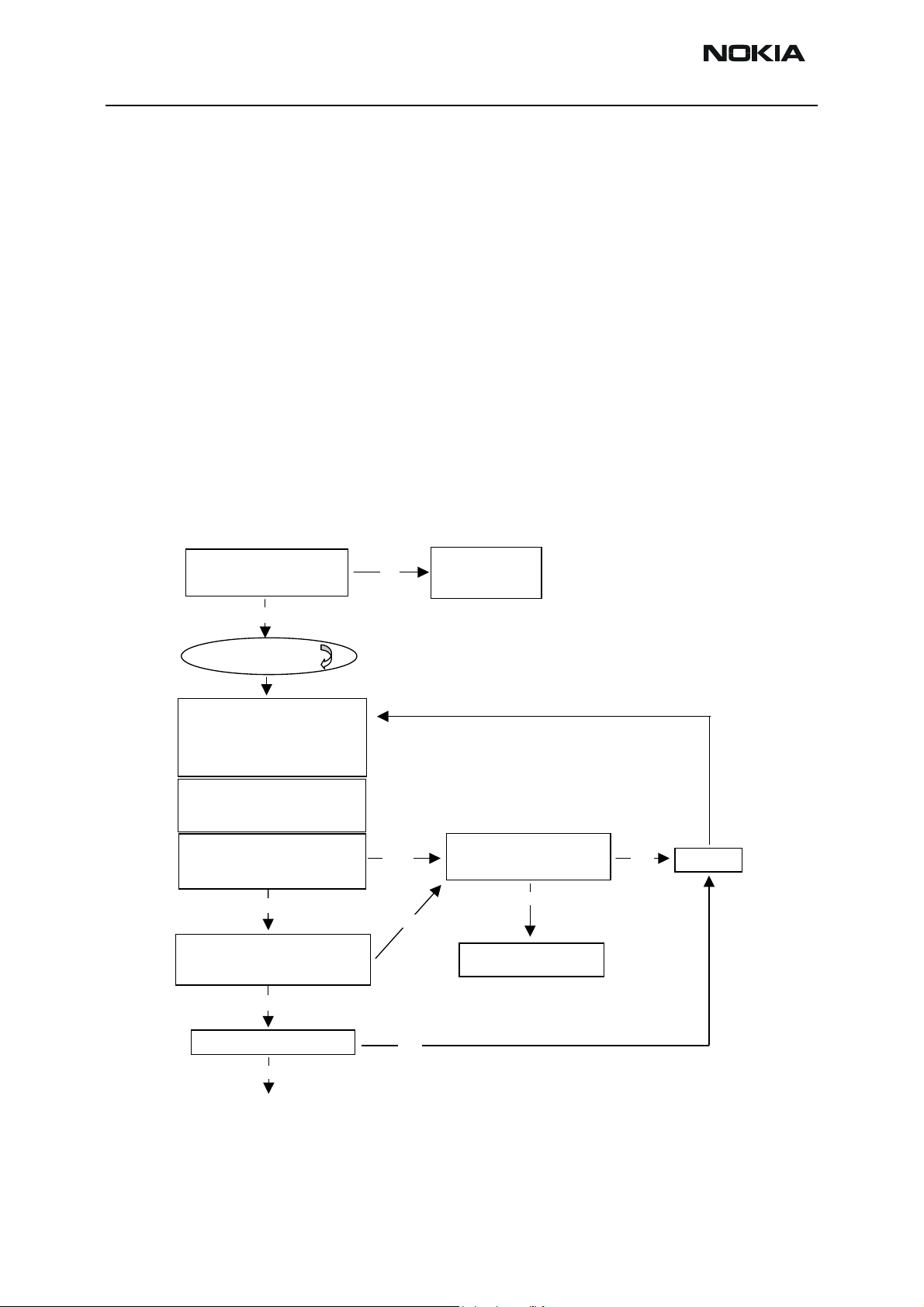
RF Troubleshooting
Introduction to RF troubleshooting
Measurements should be done using Spectrum analyzer with high-frequency highimpedance passive probe (LO-/reference frequencies and RF power levels) and Oscilloscope with a 10:1 probe (DC-voltages and low frequency signals)
The RF-section is built around one RF-ASIC (Helgo N500). For easier troubleshooting, this
RF troubleshooting document is divided in to sections.
Before changing Helgo, please check following things: Supply voltages are OK and serial
communication is coming from baseband to Helgo.
Please note that the grounding of the PA module is directly below PA-module so it is difficult to check or change. Most RF semiconductors are static discharge sensitive! So
ESD protection must be taken care of during repair (ground straps and ESD soldering
irons). Helgo and PA are moisture sensitive so parts must be pre-baked prior to soldering.
Apart from key components described in this document here are a lot of discrete components (resistors, inductors and capacitors) which troubleshooting is done by checking if
soldering of the component is done properly (for factory repairs checking if it is missing
from PWB). Capacitor can be checked for shortening and resistors for value by means of
an ohmmeter, but be aware in-circuit measurements should be evaluated carefully.
Please be aware that all measured voltages or RF levels in this document are rough figures. Especially RF levels varies due to different measuring equipment or different
grounding of the used probe. When using RF probe usually a good way is to use metallic
tweezers to connect probe ground to PWB ground as close to measurement point as possible.
Issue 1 05/04 Copyright © 2004 Nokia Corporation. All rights reserved. Page 7
Page 8
NPL-4/5 Company confidential
Troubleshooting Instructions Nokia Customer Care
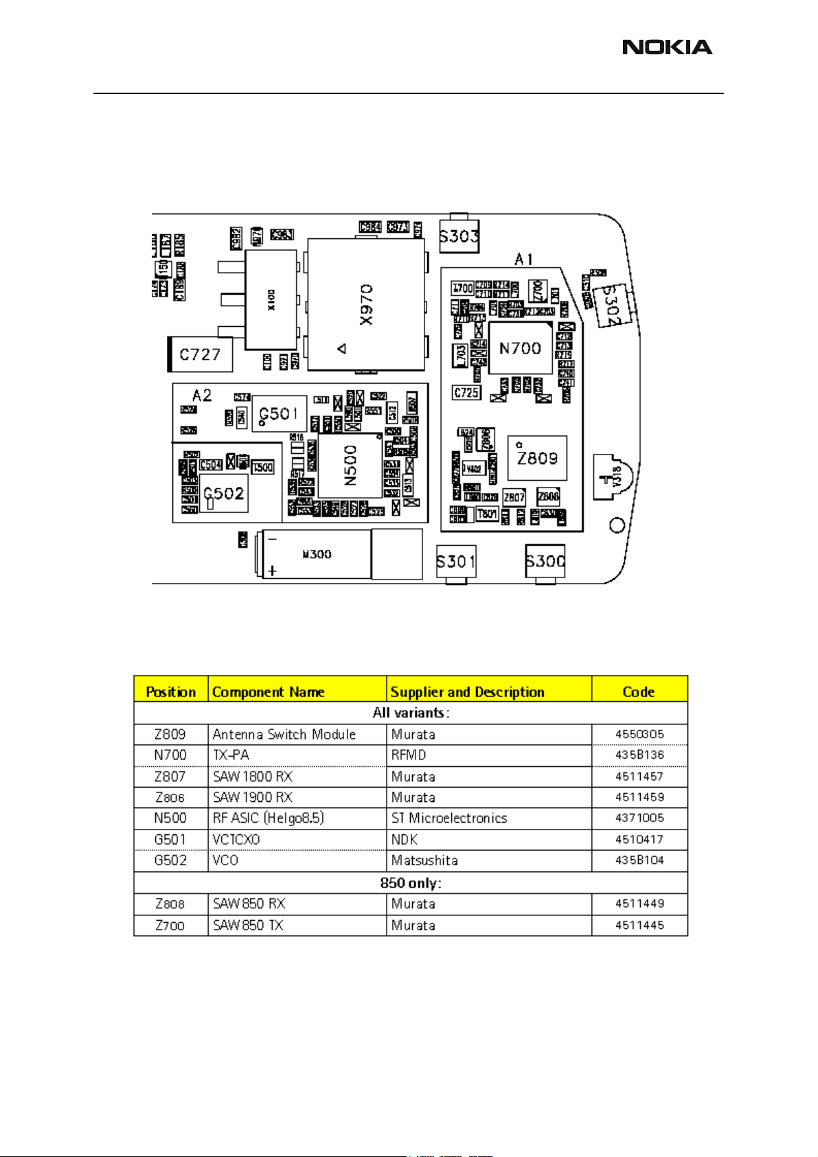
RF Key component placement
Figure 1: Component placement 1
Page 8 Copyright © 2004 Nokia Corporation. All rights reserved. Issue 1 05/04
Page 9
Company confidential NPL-4/5
Nokia Customer Care Troubleshooting Instructions
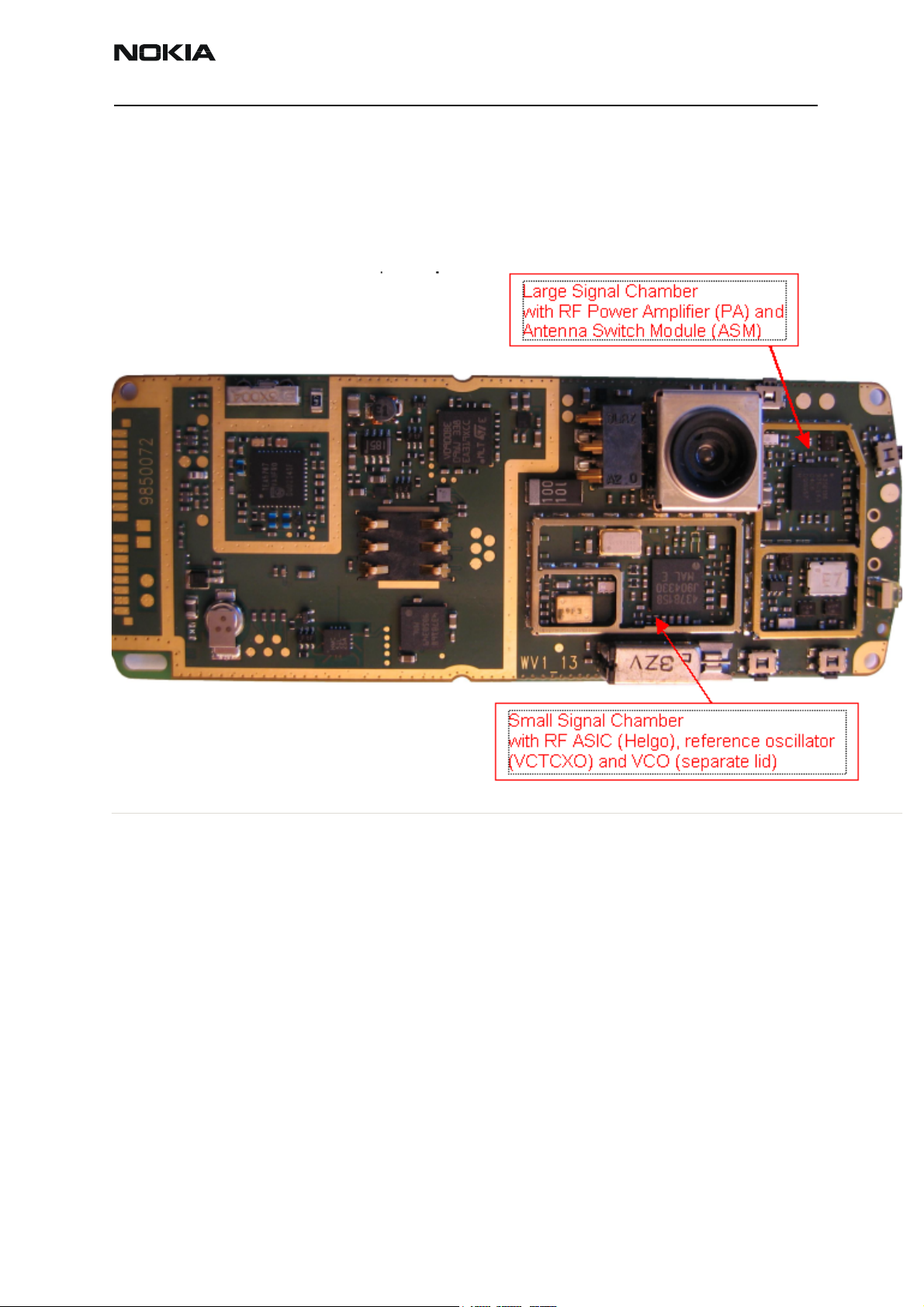
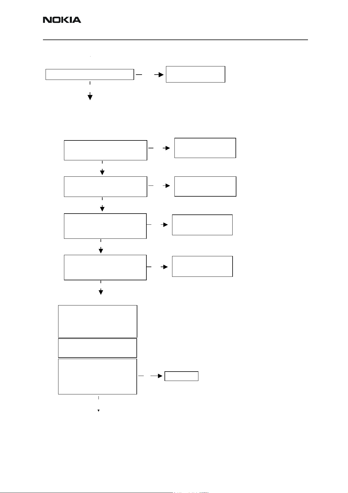
RF Test Points
The RF power supplies are generated in the UEM and can be measured either in the Small
Signal Chamber or in the Baseband Chamber. On the drawings below small points show
the locations of the test points.
Figure 2: Picture of the Assembled PWB with Chambers
Issue 1 05/04 Copyright © 2004 Nokia Corporation. All rights reserved. Page 9
Page 10
NPL-4/5 Company confidential
Troubleshooting Instructions Nokia Customer Care
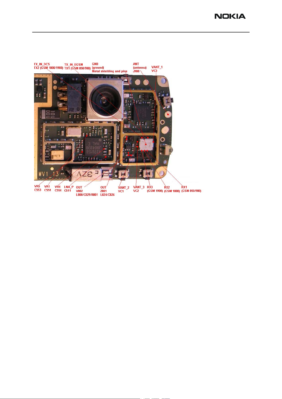
Receiver
Figure 3: Receiver Test Points
Page 10 Copyright © 2004 Nokia Corporation. All rights reserved. Issue 1 05/04
Page 11
Company confidential NPL-4/5
Nokia Customer Care Troubleshooting Instructions
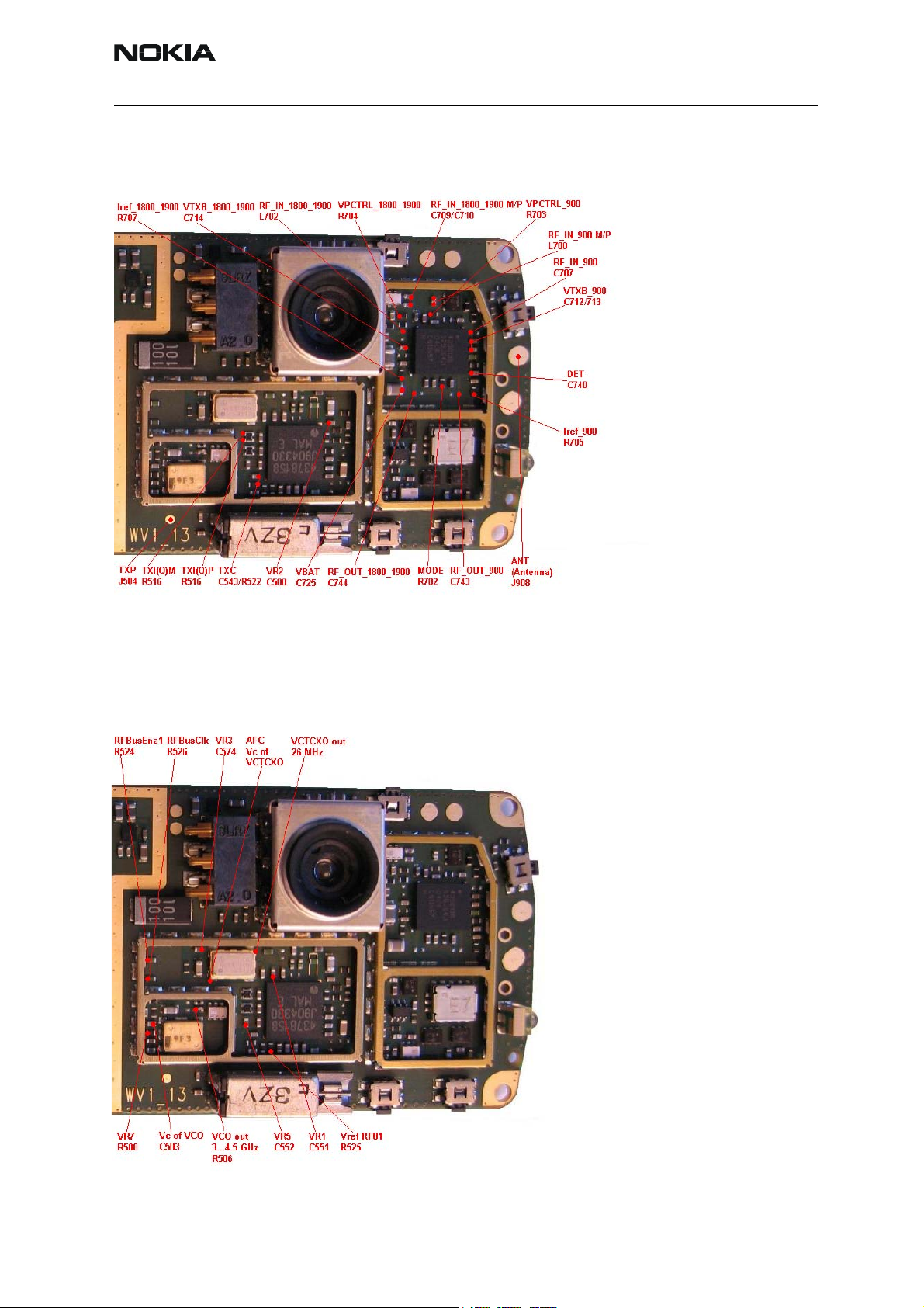
Transmitter
Figure 4: Transmitter Test Points
Synthesizer
Figure 5: Synthesizer Test Points
Issue 1 05/04 Copyright © 2004 Nokia Corporation. All rights reserved. Page 11
Page 12
NPL-4/5 Company confidential
Troubleshooting Instructions Nokia Customer Care
RF in General
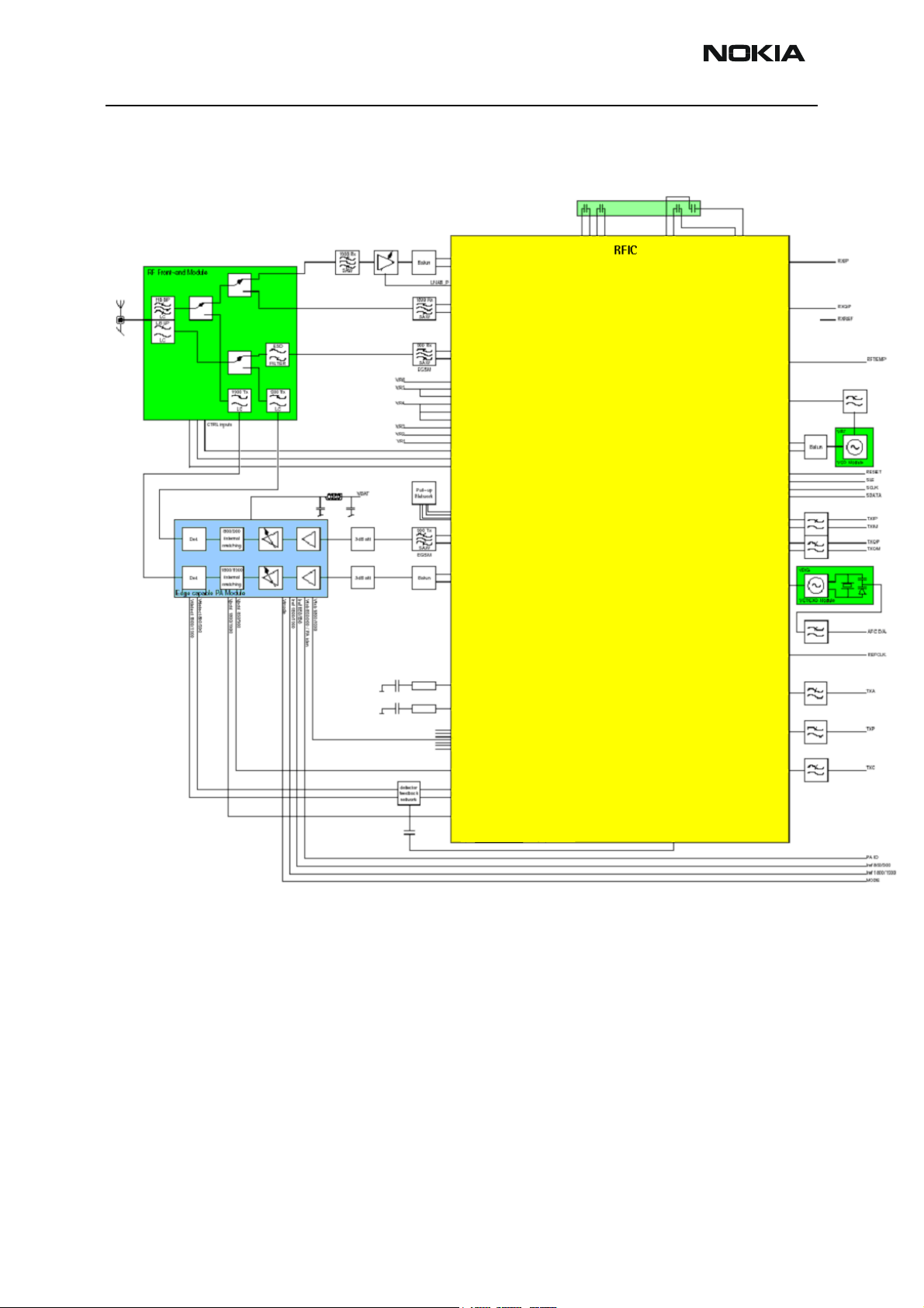
Figure 6: RF Block -Diagram
RF block diagram consisting of:
• RF front-end module
• Power amplifier module
•RF ASIC
• VCTCXO module
• VCO module
Page 12 Copyright © 2004 Nokia Corporation. All rights reserved. Issue 1 05/04
Page 13
Company confidential NPL-4/5
Nokia Customer Care Troubleshooting Instructions
The RF front-end is a triple-band direct conversion transceiver. Using direct conversion,
no intermediate frequencies are used for up- or down-conversion.
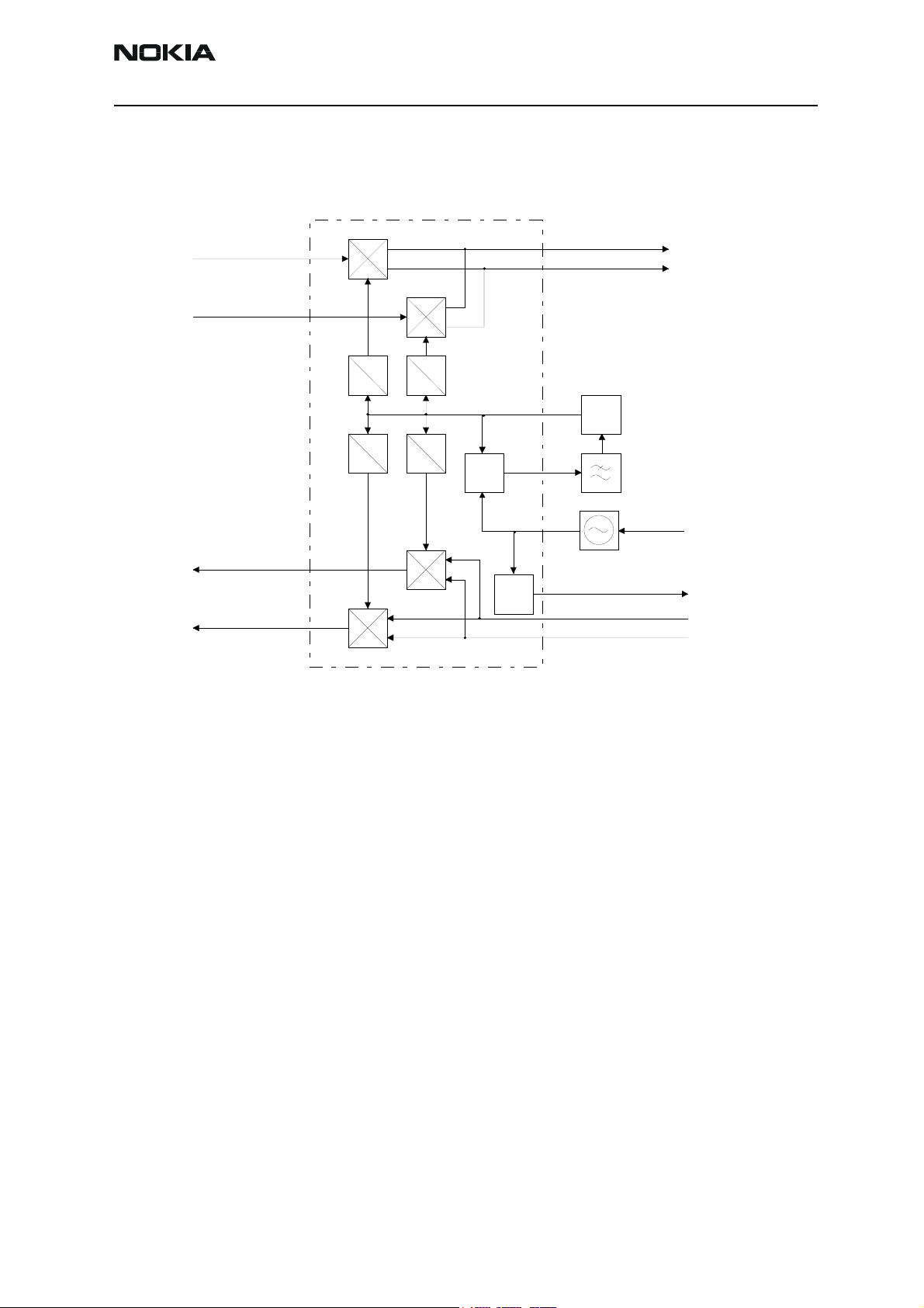
Figure 7: RF Power Supply Configuration
GSM: 869- 894 MHz
925-960 MHz
DCS: 1805-1880 MHz
PCS: 1930-1990 MHz
Helgo
I-signal
Q-signal
RX
DCS: 1710-1785 MHz
PCS: 1850-1910 MHz
GSM: 824-849 MHz
880-915 MHz
f/4
f
f
f/4
f/2
f
32963980
MHz
f
f/2
PLL
Buffer
26 MHz
VCTCXO
AFC
VCTCXO
26 MHz
I-signal
Q-signal
TX
Issue 1 05/04 Copyright © 2004 Nokia Corporation. All rights reserved. Page 13
Page 14
NPL-4/5 Company confidential
Troubleshooting Instructions Nokia Customer Care
RF Power Supply Configuration
General Specifications of Transceiver
Parameter Unit
Cellular System GSM850/900, GSM1800, GSM1900
Modulation schemes GMSK, 8-PSK
RX Frequency Band GSM850:824 … 849 MHz
GSM900:925 … 960 MHz
GSM1800:1805 ... 1880 MHz
GSM1900:1930 … 1990 MHz
TX Frequency Band GSM850:869 … 894 MHz
GSM900:880 … 915 MHz
GSM1800:1710 ... 1785 MHz
GSM1900:1850 … 1910 MHz
Output Power GMSK GSM850:+5 … +33 dBm (3.2 mW … 2 W)
GSM900:+5 … +33 dBm (3.2 mW … 2 W)
GSM1800:+0 … +30 dBm (1.0 mW … 1 W)
GSM1900:+0 … +30 dBm (1.0 mW … 1 W)
Output Power 8-PSK GSM850:+5 … 27 dBm (3.2 mW … 0.5 W)
GSM900:+5 … 27 dBm (3.2 mW … 0.5 W)
GSM1800:+0 … 26 dBm (1.0 mW … 0.4 W)
GSM1900:+0 … 26 dBm (1.0 mW … 0.4 W)
Duplex Spacing GSM850:45 MHz
GSM 900:45 MHz
GSM 1800:95 MHz
GSM 1900:80 MHz
Number of RF Channels GSM 850:124
GSM 900:174
GSM 1800:374
GSM1900:299
Channel Spacing 200 kHz (each band)
Number of TX Power Levels
GMSK
EGSM:15
GSM 900:15
GSM 1800:16
GSM 1900:16
Number of TX Power Levels
8-PSK
Sensitivity, static channel
(+25°C)
GSM 850:12
GSM 900:12
GSM 1800:14
GSM 1900:14
EGSM:-102 dBm
GSM 900:-102 dBm
GSM 1800:-102 dBm
GSM 1900:-102 dBm
Page 14 Copyright © 2004 Nokia Corporation. All rights reserved. Issue 1 05/04
Page 15
Company confidential NPL-4/5
Nokia Customer Care Troubleshooting Instructions
Frequency Error, static channel < 0.1 ppm
RMS Phase Error < 5.0 °
Peak Phase Error < 20.0 °
Issue 1 05/04 Copyright © 2004 Nokia Corporation. All rights reserved. Page 15
Page 16

NPL-4/5 Company confidential
Troubleshooting Instructions Nokia Customer Care
Receiver Verification and Troubleshooting
General instructions for RX troubleshooting
Connect the phone to a PC, which has Phoenix Service Software and a dongle installed,
using either
• Repair jig and DAU-9S (RS232) cable or
• DAU-9T cable (RS232) or
• DKU-5 cable (USB)
Connect the phone to a power supply (DC voltage: 4.0V, max. current: 3A) and an RF signal generator. Switch the phone on.
Start Phoenix Service Software and open FBUS connection.
- Select → Scan Product (Ctrl-R)
Wait until phone information (NPL-4 or NPL-5) is shown in the lower right corner of the
screen.
Follow the instructions below.
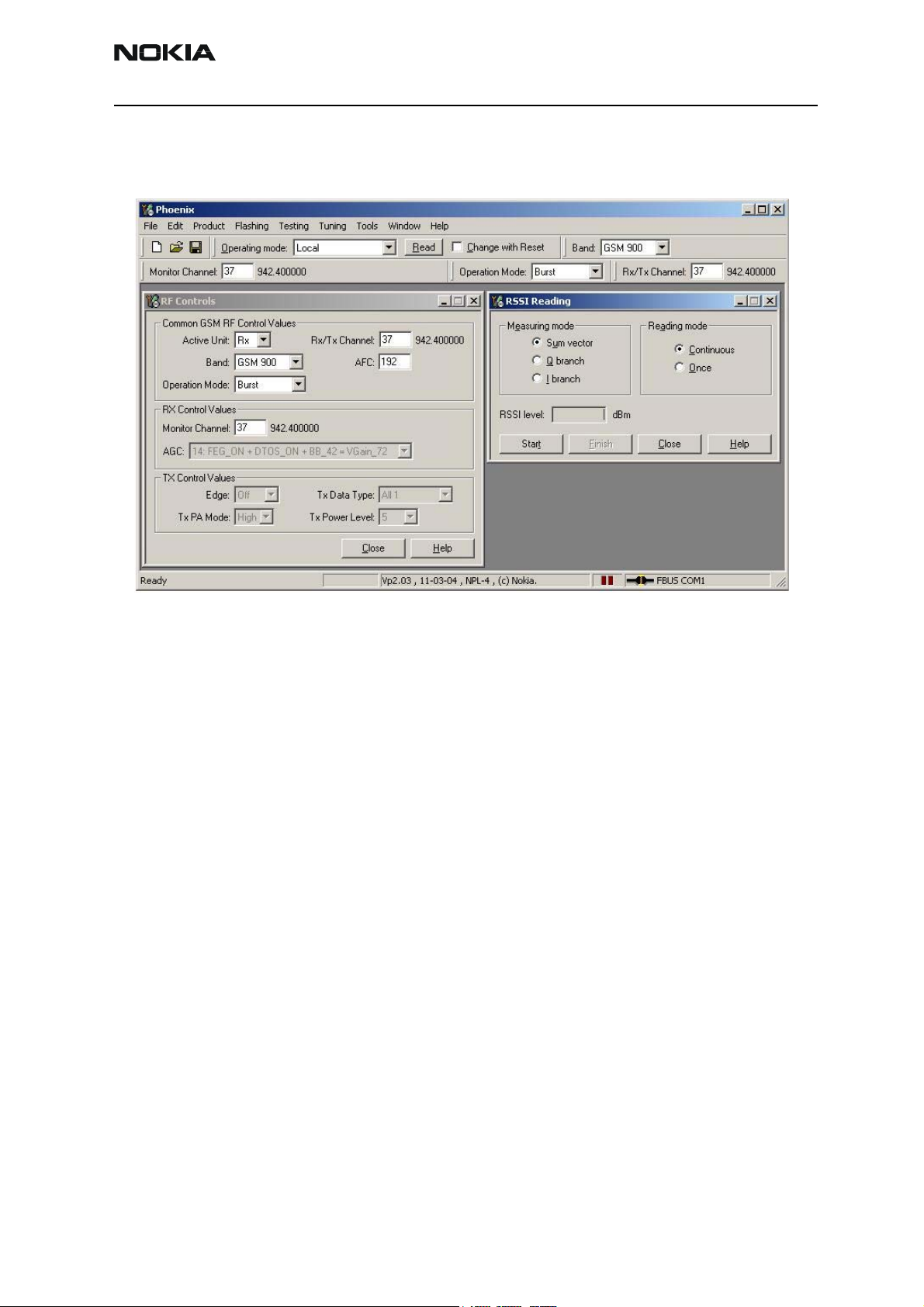
Measuring RX I/Q Signals using RSSI Reading
- Start Phoenix Service Software and open FBUS connection.
- Select → Scan Product (Ctrl-R)
Wait until phone information is shown in the lower right corner of the screen.
- Set operating mode to local mode
- Select → Testing → RF Controls
- Select → Band → GSM 850 or GSM 900 or GSM1800 or GSM1900
Active unit → RX
Operation mode → Burst
RX/TX Channel → 190 or 37 or 700 or 661
- Select → Testing → RSSI reading
In the RSSI Reading window the “measuring mode” shall be set on Sum vector and the
“reading mode” on Continuous.
Page 16 Copyright © 2004 Nokia Corporation. All rights reserved. Issue 1 05/04
Page 17
Company confidential NPL-4/5
Nokia Customer Care Troubleshooting Instructions
The set up should now look like this:
Figure 8: RSSI Window
- Make the following settings on your signal generator:
Frequencies:
• GSM 850: 869.26771 MHz (channel 190 + 67.710 kHz offset)
• GSM 900: 942.46771 MHz (channel 37 + 67.710 kHz offset)
• GSM 1800: 1842.86771 MHz (channel 700 + 67.710 kHz offset)
• GSM 1900: 1960.06771 MHz (channel 661 + 67.710 kHz offset)
2. RF power level:
– 60 dBm @ the antenna connector of the phone/ test jig
(Remember to compensate for the cable and jig attenuation).
- Click on “Read now” in RSSI reading.
The resulting RSSI level shall be – 60 dBm +/– 0.5 dB in each band.
Issue 1 05/04 Copyright © 2004 Nokia Corporation. All rights reserved. Page 17
Page 18

NPL-4/5 Company confidential
Troubleshooting Instructions Nokia Customer Care
Measuring RX performance using SNR measurement
- Start Phoenix Service Software and open FBUS connection.
- Select → Scan Product (Ctrl-R)
Wait until phone information is shown in the lower right corner of the screen.
- Set operating mode to “local mode”.
- Select → Testing → RF Controls
- Select → Band → GSM 850 or GSM 900 or GSM1800 or GSM1900
Active unit → RX
Operation mode →Burst
RX/TX Channel → 190 or 37 or 700 or 661
- Select → Testing → SNR Measurement
- Select → Measuring mode → Fast SNR (Radio Button)
- Press → Start
The window “Signal Measurement” pops up informing on frequency and power level of
the signal generator to be set.
- Press “ok” and the window will close.
- Read the SNR results.
The values should exceed:
• GSM 850: > 20 dB
• GSM 900: > 20 dB
• GSM 1800: > 18 dB
• GSM 1900: > 18 dB
The set up should now look like this:
Page 18 Copyright © 2004 Nokia Corporation. All rights reserved. Issue 1 05/04
Page 19
Company confidential NPL-4/5
Nokia Customer Care Troubleshooting Instructions
Figure 9: Signal Measurement
- Choose the remaining GSM bands and measure accordingly the procedure described
above.
Measuring front-end power levels using spectrum analyzer
Spectrum Analyzer (SA) level values depend on the probe type and shall be verified by a
properly working phone sample.
- Start Phoenix Service Software and open FBUS connection.
- Select → Scan Product (Ctrl-R)
Wait until phone information is shown in the lower right corner of the screen.
- Set operating mode to “local mode”
- Select → Testing → RF Controls
- Select → Band → GSM850 or GSM 900 or GSM1800 or GSM1900
Active unit → RX
Operation mode → Continuous
RX/TX Channel → 190 or 37 or 700 or 661
Issue 1 05/04 Copyright © 2004 Nokia Corporation. All rights reserved. Page 19
Page 20
NPL-4/5 Company confidential
Troubleshooting Instructions Nokia Customer Care
Measuring analogue RX I/Q signals using oscilloscope
Measuring with an oscilloscope on “RXIINN”, (R421) or “RXQINN”, (R423) is recommended only if RSSI reading does not provide enough information. Input level = -60dBm.
- Start Phoenix Service Software and open FBUS connection.
- Select → Scan Product (Ctrl-R)
Wait until phone information is shown in the lower right corner of the screen.
- Set operating mode to “local mode”
- Select → Testing → RF Controls
Wait until the RF Controls window is popped up.
- Select → Band →GSM 850 or GSM 900 or GSM1800 or GSM1900
Active unit → RX
Operation mode → continuous
RX/TX Channel → 190 or 37 or 700 or 661
AGC → 12
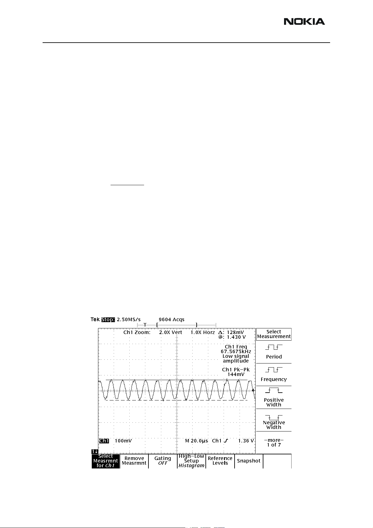
Following diagram should be displayed on an oscilloscope' s screen if the GSM 900
receiver is working properly:
Figure 10: Signal Amplitudes
Page 20 Copyright © 2004 Nokia Corporation. All rights reserved. Issue 1 05/04
Page 21
Company confidential NPL-4/5
Nokia Customer Care Troubleshooting Instructions
Correct signal amplitudes approximately
GSM850/900: ~140-150mVpp
GSM1800/1900: ~130-150mVpp
Signal frequency 67.7kHz
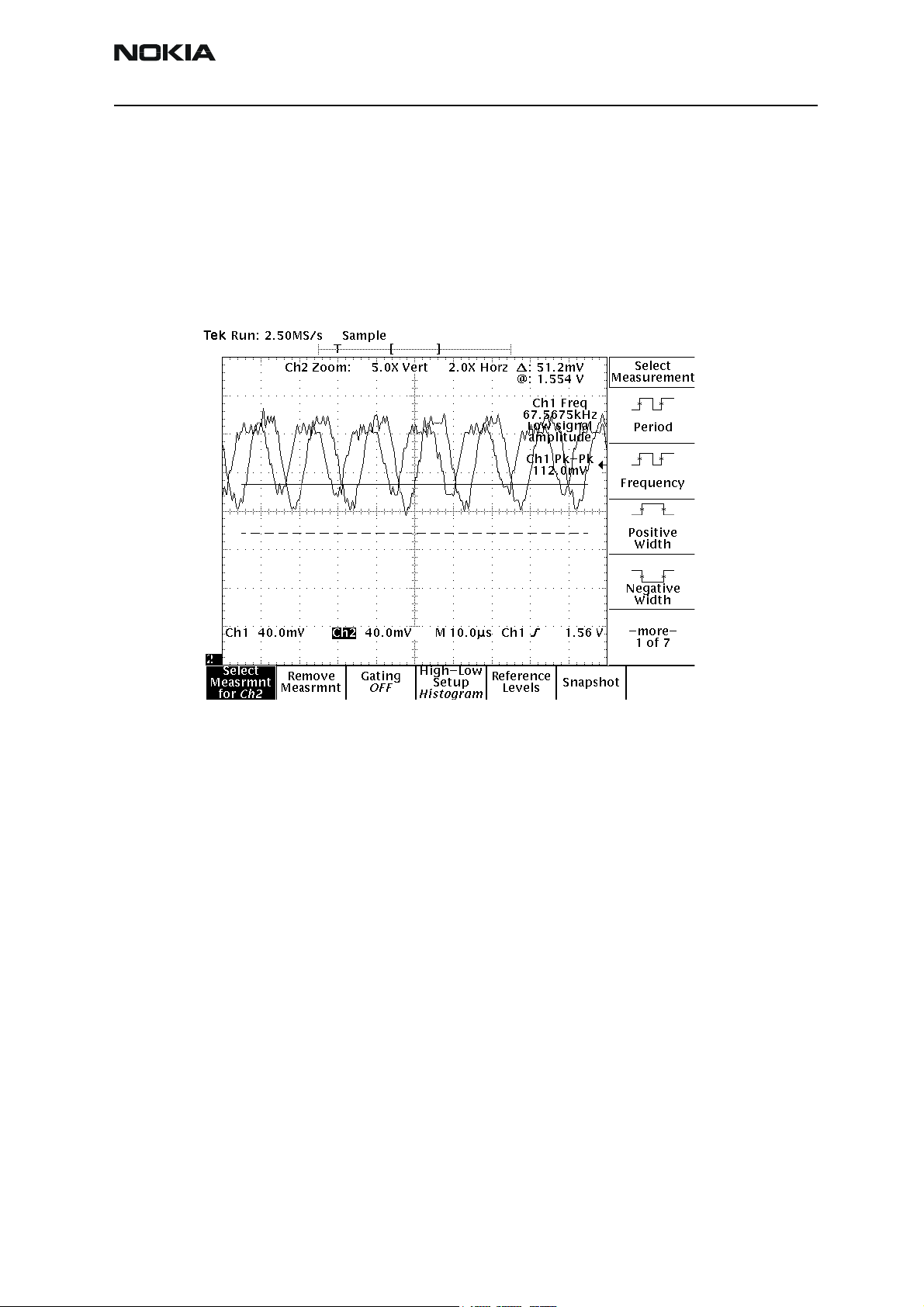
Figure 11: RX IQ Signals
RX I/Q, phase difference 90 degrees between signals.
RX I/Q-signals measured from R423 (Q-signal), R421 (I-signal) simultaneously.
Used channel 37, input signal 942.467 MHz, level –60 dBm at antenna port, AGC setting
12.
Phase difference should be 90 degrees between RX I/Q-signals at all bands.
Fault finding chart of the receiver
During fault finding, the calibration procedure is used to find out, whether all bands are
affected (error in common part of the Rx chain) or only one band (error in a Rx part of
the failed band). Take care not to save calibration values to the phone memory,
which are out of limits. Find the error first and repair it.
When a defective phone has been calibrated, a possible error in RX front-end might be
masked. In that case one can get a reasonable RSSI reading, although the front-end
shows excessive losses. If it is not sure that incorrect re-calibration has been made, following steps shall be done:
Issue 1 05/04 Copyright © 2004 Nokia Corporation. All rights reserved. Page 21
Page 22
NPL-4/5 Company confidential
A
A
A
Troubleshooting Instructions Nokia Customer Care
- Check if AGC calibration is within limits
- Check if SNR reading is OK.
- Use an Oscilloscope to check levels of “RXI” and “RXQ”.
The RF ASIC generates only single ended I and Q signals (RXI, RXQ). As the A/D converter
in UEM requires two differential signals, an artificial mid voltage is generated from
VrefRF02.
The BB part is used to measure those signals by means of RSSI reading. This works only if
correct calibration has been carried out in production.
RSSIreading [dBm] = 20log(UBB/U
LSB
) - AGC
calibrated
If both RX and TX path seem to be faulty it has to be checked if the synthesizer is working.
Figure 12: Receiver Fault Chart 1
Phoenix:
Phone: local mode
Open
Signal Gener a t o r:
Phoenix:
Open
Check RSSI Level = -80dBm
Make sure that
Synthesizer is working
Yes
All 3 bands
RF Controls
Active Unit: Rx
Op. Mode: Burst
Rx/Tx channel: default (mid)
Level: –80dBm
Frequency: calculated from
Phoenix + 67.71kHz
RSSI reading
:
No
Yes Next band No
see
Synthesizer Fault
Finding Tree
Selected band is working and
calibrated.
re all 3 bands measured?
Receiver
Fault Chart 1.
No
Execute Rx Calibration in select ed
band
re calibration results within limits?
No
re all 3 bands measured?
Yes
Yes
No
Yes
Rx chain is functional
and calibrated
Page 22 Copyright © 2004 Nokia Corporation. All rights reserved. Issue 1 05/04
Page 23
Company confidential NPL-4/5
Nokia Customer Care Troubleshooting Instructions
Figure 13: Receiver Fault Chart 2
Are all 3 bands defective?
Yes
Oscilloscope:
Check supply voltages of RF ASIC:
VR4 = 2.8V
Oscilloscope:
Check supply voltages of RF ASIC:
VR6 = 2.8V
Oscilloscope:
Check reference voltages of RF part:
VrefRF01 = 1.4V
No
Continue with single
band fault finding.
Receiver
Fault Chart 2.
Figure 14: Receiver Fault Chart 3, 4, 5
Yes
Yes
No
No
No
Check supply filter
components (C297, C554)
and UEM
Check supply filter
components (C225, C555)
and UEM
Check supply filter
components (R525, C549)
Receiver
Fault Chart 3.
Receiver
Fault Chart 4.
Yes
Oscilloscope:
Check reference voltages of RF part:
VrefRF02 = 1.4V
Yes
Phoenix:
Phone: local mode
RF Controls
Active Unit: Rx
Op. Mode:
Rx/Tx channel: default (mid)
AGC: 12
Signal Generator:
Level: –55dBm
Frequency: calculated from Phoenix
no offset
Spectrum Anal yzer: 1)
Check Rx/Tx Switch (Diplexer)
Depending on selected band, check
GSM850/900 output Rx1
GSM1800 output Rx2
GSM1900 output Rx3
Level at Z809 output > -75dBm
:
Continuous
Yes
Ye s
No
No
Check supply filter
components (R421, R423,
C421, C422) and UEM
Receiver
Fault Chart 5.
Change Z809
Note! 1) RF levels are dependent on RF probe
Note 1):
RF levels are dependent on RF probe and have to be validated
and have to be validated with a known good
with a known good sample.
sample.
Issue 1 05/04 Copyright © 2004 Nokia Corporation. All rights reserved. Page 23
Page 24
NPL-4/5 Company confidential
q
Troubleshooting Instructions Nokia Customer Care
Figure 15: Receiver Fault Chart 6
Oscilloscope:
RX IQ levels ok (RXI, RXQ)?
Yes
No
Change RF
ASIC (Helgo)
Receiver
Fault Chart 6.
Oscilloscope:
RF-BB serial interface ok?
Select faulty band in Phoenix and continue measurements on dedicated Rx part.
Phoenix:
SNR Measurement
open
Meas. Mode: Fast SNR
Measure
Press
Signal Generator:
Level: –92dBm
Fre
uency: calculated from Phoenix
Phoenix:
SNR measurement ok?
(SNR > 18.37dB)
No
.
No
Yes
Check UPP
Change RF
ASIC (Helgo)
Figure 16: Receiver Fault Chart 7
Single band fault finding
BB error:
Yes
Front end is ok.
Phoenix:
Phone: local mode
RF Controls
Active Unit: Rx
Op. Mode:
Rx/Tx channel: default (mid)
AGC: 12
Signal Generator:
Level: –55dBm
Frequency: calculated from Phoenix
no offset
:
Continuous
Continue with Rx Fault Chart 6.
Receiver
Fault Chart 7.
Page 24 Copyright © 2004 Nokia Corporation. All rights reserved. Issue 1 05/04
Page 25
Company confidential NPL-4/5
g
Nokia Customer Care Troubleshooting Instructions
Figure 17: Receiver Fault Chart 8
Phoenix:
Phone: local mode
RF Controls
Active Uni t: Rx
Op. Mode:
Rx/Tx channel: defaul t ( mid)
AGC: 12
Signal Generator:
Level: –55dBm
Frequency: calculated from Phoenix
(no offset)
Spectrum Analyzer: 1)
Center Freq: calculated from Phoenix
RBW 20kHz
Check Rx SAW filter of selected band:
GSM850/900 Z808
output both lines > -80dBm
GSM1800 Z807
output both lines > -80dBm
GSM1900 Z806
single output > -74dBm
:
Continuous
Yes
No
Change Rx SAW
(Z806, Z807, Z808)
depending on selected band
Note 1):
Note! 1) RF levels are dependent on RF probe
RF levels are dependent on RF probe and have to be valid ated
and have to validated with a known good sample.
with a known good sample.
Receiver
Fault Chart 8.
If selected band = GSM1900
No
Spectrum Analyzer:
Check external LNA V802:
Output signal pin 3 > - 56dBm
Spectrum Analyzer: 1)
Check balun T801:
Both output signals at pin 3+4 > - 62dBm
RF ASIC N500 seems to be
defective. Exchange N500.
Yes
Yes
Yes
Figure 18: Receiver Fault Chart 9
1)
Change V802
Oscilloscope:
Check voltages for V802:
No
No
Voltage at C827 = 2.6V
Volta
e at C801 = 0V
Yes
Note 1):
Note! 1) RF levels are dependent on RF probe
RF levels are dependent on RF probe and have to be validated
and have to validated with a known good sample.
with a known good sample.
No
Receiver
Fault Chart 9.
No
Check supply
filter components
around V802 and
RF ASIC N500
Change T801
Rx signal paths
Antenna switch (RX/TX switch)
RF signal is fed directly from the antenna-pad (J908) to the antenna switch (Z809).
This switch has the function of a diplexer, which consists of two combined paths (low
pass/high pass filter combination), a GSM850/900 and a GSM1800/1900 path. The GSM
850/900 input signals pass the switch to the Rx1 output. Via a switch the GSM 1800
input signals pass to Rx2 output and GSM 1900 to Rx3 output, depending on the control
Issue 1 05/04 Copyright © 2004 Nokia Corporation. All rights reserved. Page 25
Page 26
NPL-4/5 Company confidential
Troubleshooting Instructions Nokia Customer Care
signal VANT3=1, whereas VANT1=VANT2=0.
• Signal paths from the antenna switch to the band filters:
GSM 850/900:RX1 Æ GSM850 SAW filter (Z808) or
Æ GSM900 SAW filter (Z808)
• GSM1800: RX2 Æ GSM1800 SAW filter (Z807)
• GSM1900: RX3 Æ GSM1900 SAW filter (Z806)
The antenna switch has following typical insertion losses in Rx-mode from its input to
output ports:
• GSM 850/900: 1.3 dB
• GSM 1800: 1.6 dB
• GSM 1900: 1.6 dB
Figure 19: Block Diagram of Antenna Switch: Left Input Port (Antenna) and Right Output Ports Rx/Tx
EGSM
RX
LPF
HPF
LPF
GSM1800
GSM1900
TX
RX
LPF
Rx front-end
The RX front-end includes three SAW filters for GSM 850 [US-variant] or GSM 900 [EUvariant] (Z808), and for both variants GSM1800 (Z807), and GSM1900 (Z806). GSM 850/
900 and GSM 1800 filters are matched to the corresponding LNA inputs of the RF ASIC
(N500) with differential matching network (LC-type). For GSM 1900 an external LNA
(V802) improves the noise figure of the receiver. For conversion of the unbalanced output
port to the balances input port of the RF ASIC the BALUN (T801) is applied, followed by a
differential matching network (LC-type). The SAW filters provide the wanted out-ofband blocking immunity. They have one single-ended (unbalanced) input port and two
balanced output ports each.
TX
The SAW filters have approximately 2.5 to 3.2 dB insertion losses. The LNA for the GSM
1900 band provides a gain of approximately 17 to 20 dB.
Page 26 Copyright © 2004 Nokia Corporation. All rights reserved. Issue 1 05/04
Page 27

Company confidential NPL-4/5
Nokia Customer Care Troubleshooting Instructions
RX paths of RF ASIC
The balanced GSM 850/900 and GSM 1800 RX signals are amplified by one integrated
LNA for each band and the subsequent pre-gain stages. The GSM 1900 signal is fed to
the pre-gain stage also used for the GSM 1800 signal. After amplification the RX signals
are down-converted.
The RX paths of the RF ASIC consist of following sub units:
• Separate LNAs for each of the bands: GSM 850/900, and GSM1800.
• Two PRE-GAIN amplifiers, one for GSM 850/900 and one for GSM1800
and GSM1900.
• Two passive I/Q mixers (MIX), one for GSM 850/900 and one for
GSM1800 and GSM1900.
Issue 1 05/04 Copyright © 2004 Nokia Corporation. All rights reserved. Page 27
Page 28

NPL-4/5 Company confidential
Troubleshooting Instructions Nokia Customer Care
Transmitter
General instructions for transmitter troubleshooting
Connect the phone to a PC, which has Phoenix Service Software and a dongle installed,
using either
• Repair jig and DAU-9S (RS232) cable or
• DAU-9T cable (RS232) or
• DKU-5 cable (USB).
Connect the phone to a power supply (DC voltage of 3.9V) and switch the phone on.
The value of the DC voltage of 3.9V at the phone battery connector is crucial.
Attention: When repairing or tunning transmitter use external DC supply with at least 3A
current capability.
Connect an RF cable between the test jig and the measurement equipment (GSM test
equipment, power meter, spectrum analyzer, or similar).
Make use of an adequate attenuator at the input of your measurement equipment (10dB
to 20dB are recommended for a spectrum analyzer or a power meter). Additionally, a DC
block is recommended. Assure not to overload or destroy the equipment.
Start Phoenix Service Software and open FBUS connection:
Select->Scan Product->Ctrl-R
and wait until phone information is shown in the lower right corner of the screen.
Follow the instructions in the chapters below.
Transmitter troubleshooting
Antenna switch (TX/RX switch)
The antenna switch operates as a diplexer for the RX and TX signals. Moreover, it suppresses the TX harmonics generated by the PA. The antenna switch is a controlled by the
RF ASIC using the control signals VANT1, VANT2 and VANT3.
The table below shows the possible different switching states.
Page 28 Copyright © 2004 Nokia Corporation. All rights reserved. Issue 1 05/04
Page 29
Company confidential NPL-4/5
Nokia Customer Care Troubleshooting Instructions
Table 1: Switching States
VANT2
VC1
[Volt]
0 0 0 X
0 0 0 X
0 0 2.7 X
0 2.7 0 X
2.7 2.7 0 X
VANT3
VC2
[Volt]
To switch the TX -GSM 1800/1900 path both signals VANT2 and VANT3 have to be activated. This increases the isolation from the TX-GSM 1800/1900 path to the RX-GSM
1800 path and reduces the feed back of RF-power to the RF ASIC.
GSM850 transmitter
GSM850 chapture is valid only for the NPL-4 (US variant). Start the preparations as
described in chapter General instruction for the transmitter troubleshooting.
VANT1
VC3
[Volt]
Rx1
GSM
900
Rx
850/
Rx2
GSM
1800
Rx
Rx3
GSM
1900
Rx
TX_IN_E
GSM
Tx1
GSM
850/
900
Tx
TX_IN_D
CS
Tx2
GSM
1800/1900
Tx
General instructions for GSM850 TX troubleshooting
GMSK
Select operating mode to “local mode”:
Select->Testing->RF Controls
In the popped up window:
Select->Band->GSM 850
-Active unit->TX
-Operation mode->Burst
-RX/TX Channel->190
-TX Power Level->10
-TX Data Type->Random
The Phoenix window should now look like this:
Issue 1 05/04 Copyright © 2004 Nokia Corporation. All rights reserved. Page 29
Page 30
NPL-4/5 Company confidential
Troubleshooting Instructions Nokia Customer Care
Figure 20: RF Controls
EDGE
Now the measurement setup, which has been built according to the Check synthesizer
Operation-chapter, should detect the following output signal of the phone.
P
= +23dBm @ 836.6 MHz
out
If this is not the case, then go to the chapter GMSK for the troubleshooting.
Start the preparations as described in chapter Check synthesizer Operation.
Select operation mode to the “local”.
Select->Testing -> RF control
In the popup window common values:
Active unit:->TX
Band: ->850
Operation mode: ->Burst
RX/TX Channel:->190
In the popup window TX control values:
EDGE:->ON
Page 30 Copyright © 2004 Nokia Corporation. All rights reserved. Issue 1 05/04
Page 31

Company confidential NPL-4/5
Nokia Customer Care Troubleshooting Instructions
Tx data type:->Alternate
TX PA mode:->High
TX Power level:->10
Issue 1 05/04 Copyright © 2004 Nokia Corporation. All rights reserved. Page 31
Page 32

NPL-4/5 Company confidential
Troubleshooting Instructions Nokia Customer Care
The Phoenix window should now look like this:
Figure 21: RF Controls
Now the measurement equipment should detect the following output signal of the
phone:
P
= +24 dBm @ 836.6 MHz
out
If this is not the case, then go to the chapter EDGE for the troubleshooting.
Start the preparations as described in Check synthesizer Operation .
Fault Finding Chart for GSM850 Transmitter
In the following, it is assumed that the TXP signal is used as trigger-signal. For that a
TXP test point is provided.
Page 32 Copyright © 2004 Nokia Corporation. All rights reserved. Issue 1 05/04
Page 33

Company confidential NPL-4/5
Nokia Customer Care Troubleshooting Instructions
GMSK
Use Phoenix to select
TX_Data Type: "1" or "0"
TX Power Level: 10
Ch190
Ensure Vbatt=3.9 V
Yes
Oscilloscope
C702
R525
C500
TXP testpoint J504
C553
C574
Yes
Oscilloscope
C529
C529
C530
C530
Yes
Oscilloscope
C713 VTXB_850 Vdc = 2.88 Volt No Check:
VC1 CONT1 Vdc = 0 Volt Helgo Ser ial Interface
VC2 CONT2 Vdc = 0 Volt Helgo
VC3 CONT3 Vdc = 2.76 Volt
R703
Yes
Spectrum analyzer No Check
C707 RFin_850/900 P>= -3 dBm,
Compare with
Yes Synthesizer
Use Phoenix to select
Use Phoenix to select
TX_Data Type: Random
TX_Data Type: Random
TX Power Level: 10
Spectrum analyzer Check PA N700
N700RFOut_850/900)
Power = +25 dBm,
Spectrum analyzer Check
= +23 dBm, 836.6MHz
Yes
Z809 TX1 (PA
836.6MHz
Yes
RF-connector No
Pout
Yes
GSM850 TX
OK
Mode
VREF01
VR2
TXP
VR5
VR3
TXIOUTP
Vdc = 1.35 Volt Check
Vdc = 2.78 Volt No Base Band
Vdc = 2.78 Volt
Vdc = 2.78 Volt
Vdc = 0 Volt
Vdc = 1.8 Volt
67kHz
No Check
Vac = 0.4 Vpp, Vdc
= 1.1 V
TXIOUTN
67kHz
Base Band
Vac = 0.4 Vpp, Vdc
TXQOUTP
= 1.1 V
67kHz
Vac = 0.4 Vpp, Vdc
= 1.1 V
TXQOUTN
67kHz
Vac = 0.4 Vpp, Vdc
= 1.1 V
VPCTRL_850 Vdc > 1.3 Volt
EGSM TX SAW Filter
836.6MHz
Helgo
good sample
No Check Power Loop
Check TXC
Antenna Switch
(Z809)
Issue 1 05/04 Copyright © 2004 Nokia Corporation. All rights reserved. Page 33
Page 34

NPL-4/5 Company confidential
Troubleshooting Instructions Nokia Customer Care
EDGE
Ensure that the GMSK is OK!
Use Phoenix to select
TX_Data Type: "1" or "0"
TX Power Level: 10
Ch190
Ensure Vbatt=3.9 V
Yes
Oscilloscope
C741
C702
BOM1 VPCTRL_900
BOM2 VPCTRL_900
Yes
Spectrum analyzer Check PA N700
RF-connector No Check Power Loop
Pout
= +24 dBm, 836.6MHz
Yes
GSM850 TX
OK
IREF01
Mode
R703
R703
Vdc > 0.5 Volt Chec k
Vdc = 2.78 Volt No Base Band
Vdc= 0 V
Vdc= 2.7 V
GSM900 transmitter
GSM900 chapter is valid only for the NPL-5 (EU variant).
General instructions for GSM TX troubleshooting
GMSK
Set the operating mode to the “local mode”.
Select-<Testing->RF Controls
Wait until the RF Controls window is popped up
Select->Band->GSM 900
-Active unit->TX
-Operation mode->Burst
-RX/TX Channel->37
-TX Power Level->10
Page 34 Copyright © 2004 Nokia Corporation. All rights reserved. Issue 1 05/04
Page 35

Company confidential NPL-4/5
Nokia Customer Care Troubleshooting Instructions
-TX Data Type->Random
The setup should now look like this:
Figure 22: Band Selection
EDGE
Now the measurement equipment should detect the following output signal of the
phone:
P
= +23dBm @ 897.4 MHz
out
If this is not the case, then go to the chapter GMSK for troubleshooting.
Select operation mode to the “local”.
Select->Testing-> RF control
In the popup window common values:
Active unit:->TX
Band: ->900
Operation mode: ->Burst
RX/TX Channel:->37
In the popup window TX control values:
Issue 1 05/04 Copyright © 2004 Nokia Corporation. All rights reserved. Page 35
Page 36

NPL-4/5 Company confidential
Troubleshooting Instructions Nokia Customer Care
EDGE:->ON
Tx data type->Alternate
TX PA mode:->High
TX Power level:->10
The setup should now look like this:
Figure 23: RF Control Values
Now the measurement equipment should detect the following output signal of the
phone:
P
= +24 dBm @ 897.4 MHz
out
If this is not the case, then go to the chapter EDGE for the troubleshooting.
Fault finding chart for GSM900 transmitter
In the following, it is assumed that the TXP signal is used as trigger-signal. For that a
TXP test point is provided.
Page 36 Copyright © 2004 Nokia Corporation. All rights reserved. Issue 1 05/04
Page 37

Company confidential NPL-4/5
Nokia Customer Care Troubleshooting Instructions
GMSK
Use Phoenix to select
TX_Data Type: "1" or "0"
TX Power Level: 10
Ch37
Ensure Vbatt=3.9 V
Yes
Oscilloscope
R702
R525
C520
TXP testpoint
C552
C574
Yes
Oscilloscope
C535
C535
C536
C536
Yes
Oscilloscope
C713
VC1
VC2
VC3
R712
Yes
Spectrum analyzer No Check
Z700 out, R706 in RFin_850/
Compare with good
Yes Synthesizer
Use Phoenix to select
TX_Data Type: Random
TX Power Level: 10
Yes
Spectrum analyzer Check PA N700
Spectrum analyzer Check PA N700
Z809TX1 (PA N700 No Check Power Loop
Z809TX1 (PA N700
RFOut_850/900)
Power = +25 dBm, 897.4
MHz
Yes
Spectrum analyzer Check
RF-connector No
Pout
= +23 dBm, 897.4 MHz
Yes
GSM900 TX
OK
Mode
VREF01
VR2
TXP
VR5
VR3
TXIOUTP
Vdc = 1.35 Volt Check
Vdc = 2.78 Volt No Base Band
Vdc = 1.8 Volt
Vdc = 2.78 Volt
Vdc = 2.78 Volt
Vdc = 0 Volt
67kHz
No Check
Vac = 0.4 Vpp, Vdc =
1.1 V
TXIOUTN
67kHz
Base Band
Vac = 0.4 Vpp, Vdc =
1.1 V
TXQOUTP
67kHz
Vac = 0.4 Vpp, Vdc =
1.1 V
TXQOUTN
67kHz
Vac = 0.4 Vpp, Vdc =
1.1 V
VTXB_900
CONT1
CONT2
CONT3
VPCTRL_90
0
Vdc = 2.78 Volt No Check:
Vdc = 0 Volt Helgo Serial Interface
Vdc = 0 Volt Helgo
Vdc = 2.7 Volt
Vdc > 1 Volt
P>= -3 dBm, 897.4MHz EGSM TX SAW Filter
900
Helgo
sample
No Check Power Loop
Check TXC
Antenna Switch (Z809)
Issue 1 05/04 Copyright © 2004 Nokia Corporation. All rights reserved. Page 37
Page 38

NPL-4/5 Company confidential
Troubleshooting Instructions Nokia Customer Care
EDGE
Ensure that the GMSK is OK!
Use Phoenix to select
TX_Data Type: "1" or "0"
TX Power Level: 10
Ch37
Ensure Vbatt= 3. 9 V
Yes
Oscilloscope
R705
R702
BOM1 VPCTRL_900
BOM2 VPCTRL_900
Yes
Spectrum analyzer Check PA N700
RF-connector No Check Power Loop
Pout
= +24 dBm, 897.4MHz
Yes
GSM900 TX
OK
IREF01
Mode
R703
R703
Vdc > 0.5 Volt Check
Vdc = 2.78 Volt No Base Band
Vdc= 0 V
Vdc= 2.7 V
GSM1800 transmitter
General instructions for GSM1800 TX troubleshooting
Start the preparations as described in chapter Check Synthesizer Operation.
GMSK
Set the operating mode to “local mode”.
Select->Testing->RF Controls
Wait until the RF Controls window is popped up
Select->Band->GSM 1800
-Active unit->TX
-Operation mode->Burst
-RX/TX Channel->700
-TX Power Level->5
Page 38 Copyright © 2004 Nokia Corporation. All rights reserved. Issue 1 05/04
Page 39

Company confidential NPL-4/5
Nokia Customer Care Troubleshooting Instructions
-TX Data Type->Random
The setup should now look like this:
Figure 24: RF Control Values
EDGE
Now the measurement equipment should detect the following output signal of the
phone:
P
= +23dBm @ 1747.8 MHz
out
If this is not the case, then go to the chapter GMSK for the troubleshooting.
Select operation mode to the “local”.
Select->Testing -> RF control
In the popup window common values:
Active unit:->TX
Band:->1800
Operation mode: ->Burst
RX/TX Channel:->700
In the popup window TX control values:
EDGE:->ON
Issue 1 05/04 Copyright © 2004 Nokia Corporation. All rights reserved. Page 39
Page 40

NPL-4/5 Company confidential
Troubleshooting Instructions Nokia Customer Care
Tx data type:->Alternate
TX PA mode:->High
TX Power level:->5
The setup should now look like this:
Figure 25: RF Control Values
Now the measurement equipment should detect the following output signal of the
phone:
P
= +21 dBm @ 1747.8 MHz
out
If this is not the case, then go to the next chapter for troubleshooting.
Fault finding chart for GSM1800 transmitter
In the following, it is assumed that the TXP signal is used as trigger-signal. For that a
TXP test point is provided.
Page 40 Copyright © 2004 Nokia Corporation. All rights reserved. Issue 1 05/04
Page 41

Company confidential NPL-4/5
Nokia Customer Care Troubleshooting Instructions
GMSK
TX_Data Type: "1" or "0"
TX Power Level: 5
Ch700
Ensure Vbatt=3.9V
Yes
Oscilloscope
R702
R525
C500
TXP testpoint
C552
C574
Yes
Oscilloscope
C535
C535
C536
C536
Yes
Oscilloscope
C709
VC1
VC2
VC3
R713
Yes
Spectrum analyzer No Check
T700 out, R710n RFin_180
Compare with good
Yes Synthesizer
Use Phoenix to select
TX_Data Type: Random
TX Power Level: 5
Yes
Spectrum analyzer Check PA N700
Spectrum analyzer Check PA N700
Z809TX2 (PA N700
Z809TX2 (PA N700
RFOut_1800/1900)
RFOut_1800/1900)
Power = +22 dBm, 1747.8
MHz
Yes
Spectrum analyzer Check
RF-connector No
Pout
= +20 dBm, 1747.8 MHz
Yes
GSM 1800 TX
OK
Mode
VREF01
VR2
TXP
VR5
VR3
TXIOUTP
Vdc = 1.35 Volt Check
Vdc = 2.78 Volt No Base Band
Vdc = 1.88 Volt
Vdc = 2.78 Volt
Vdc = 2.78 Volt
Vdc = 0 Volt
67kHz
No Check
Vac = 0.4 Vpp, Vdc =
1.1 V
TXIOUTN
67kHz
Base Band
Vac = 0.4 Vpp, Vdc =
1.1 V
TXQOUTP
67kHz
Vac = 0.4 Vpp, Vdc =
1.1 V
TXQOUTN
67kHz
Vac = 0.4 Vpp, Vdc =
1.1 V
VTXB_1800
_1900
CONT1
CONT2
CONT3
VPCTRL_18
00_1900
Vdc = 2.78 Volt No Check:
Vdc = 2.7 Volt Helgo Serial Interface
Vdc = 2.7 Volt Helgo
Vdc = 0 Volt
Vdc > 1 Volt
P>= -3 dBm, 1747.8MHz T700 Balun
0/1900
Helgo
sample
No Check Power Loop
No Check Power Loop
Check TXC
Antenna Switch (Z809)
Issue 1 05/04 Copyright © 2004 Nokia Corporation. All rights reserved. Page 41
Page 42

NPL-4/5 Company confidential
Troubleshooting Instructions Nokia Customer Care
EDGE
Ensure that the GMSK is OK!
Use Phoenix to select
TX_Data Type: "1" or "0"
TX Power Level: 5
Ch700
Ensure Vbatt=3.9V
Yes
Oscilloscope
C742
C702
BOM1 VPCTRL_1800
BOM2 VPCTRL_1800
Yes
Spectrum analyzer Check PA N700
RF-connector No Check Power Loop
Pout
= +21 dBm, 1747.8 MHz
Yes
GSM 1800 TX
OK
IREF_1800_
1900
Mode
R713
R713
Vdc > 0.5 Volt Check
Vdc = 2.78 Volt No Base Band
Vdc= 0 V
Vdc= 2.7 V
GSM1900 transmitter
General instructions for GSM1900 TX troubleshooting
GMSK
Set the operating mode to “local mode”.
Select->Testing->RF Controls
Wait until the RF Controls window is popped up
Select->Band->GSM 1900
-Active unit->TX
-Operation mode->Burst
-RX/TX Channel->661
-TX Power Level->5
-TX Data Type->Random
Page 42 Copyright © 2004 Nokia Corporation. All rights reserved. Issue 1 05/04
Page 43

Company confidential NPL-4/5
Nokia Customer Care Troubleshooting Instructions
The setup should now look like this:
Figure 26: RF Control Values
EDGE
Now the measurement equipment should detect the following output signal of the
phone:
P
= +23dBm @ 1880 MHz
out
If this is not the case, then go to the chapter GMSK for the troubleshooting.
Select operation mode to the “local”.
Select->Testing -> RF control
In the popup window common values:
Active unit:->TX
Band: ->1900
Operation mode: ->Burst
RX/TX Channel:->661
In the popup window TX control values:
EDGE:->ON
Tx data type:->Alternate
TX PA mode:->High
Issue 1 05/04 Copyright © 2004 Nokia Corporation. All rights reserved. Page 43
Page 44

NPL-4/5 Company confidential
Troubleshooting Instructions Nokia Customer Care
TX Power level:->5
The setup should now look like this:
Figure 27: RF Control Values
Now the measurement equipment should detect the following output signal of the
phone:
P
= +21 dBm @ 1880 MHz
out
If this is not the case, then go to the chapter EDGE for the troubleshooting.
Fault finding chart for GSM1900 transmitter
In the following, it is assumed that the TXP signal is used as trigger-signal. For that a
TXP test point is provided.
Page 44 Copyright © 2004 Nokia Corporation. All rights reserved. Issue 1 05/04
Page 45

Company confidential NPL-4/5
Nokia Customer Care Troubleshooting Instructions
GMSK
Use Phoenix to select
TX_Data Type: "1" or "0"
TX Power Level: 5
Ch661
Ensure Vbatt=3.9 V
Yes
Oscilloscope
R702
R525
C500
TXP testpoint
C552
C526
Yes
Oscilloscope
C535
C535
C536
C536
Yes
Oscilloscope
C714
VC1
VC2
VC3
R713
Yes
Spectrum analyzer No Check
T700 out, R710 in RFin_180
Compare with good
Yes Synthesizer
Use Phoenix to select
TX_Data Type: Random
TX Power Level: 5
Yes
Spectrum analyzer Check PA N700
Spectrum analyzer Check PA N700
Z809 TX2 (PA N700
Z809 TX2 (PA N700 No Check Power Loop
RFOut_1800/1900)
Power = +22 dBm, 1747.8
MHz
Yes
Spectrum analyzer Check
RF-connector No
Pout
= +20 dBm, 1747.8 MHz
Yes
GSM 1800 TX
OK
Mode
VREF01
VR2
TXP
VR5
VR3
TXIOUTP
Vdc = 0 Volt
Vdc = 1.35 Volt Check
Vdc = 2.78 Volt No Base Band
Vdc = 1.8 Volt
Vdc = 2.78 Volt
Vdc = 2.78 Volt
67kHz
No Check
Vac = 0.4 Vpp, Vdc =
1.1 V
TXIOUTN
67kHz
Base Band
Vac = 0.4 Vpp, Vdc =
TXQOUTP
1.1 V
67kHz
Vac = 0.4 Vpp, Vdc =
1.1 V
TXQOUTN
67kHz
Vac = 0.4 Vpp, Vdc =
1.1 V
VTXB_1800
_1900
CONT1
CONT2
CONT3
VPCTRL_18
00_1900
Vdc = 2.78 Volt No Check:
Vdc = 2.7 Volt Helgo Serial Interface
Vdc = 2.7 Volt Helgo
Vdc = 0 Volt
Vdc > 1 Volt
P>= -3 dBm, 1747.8MHz T700 Balun
0/1900
Helgo
sample
No Check Power Loop
Check TXC
Antenn a Switch (Z809)
Issue 1 05/04 Copyright © 2004 Nokia Corporation. All rights reserved. Page 45
Page 46

NPL-4/5 Company confidential
Troubleshooting Instructions Nokia Customer Care
EDGE
Ensure that the GMSK is OK!
Use Phoenix to select
TX_Data Type: "1" or "0"
TX Power Level: 5
Ch661
Ensure Vbatt=3.9 V
Yes
Oscilloscope
C742
C702
BOM1 VPCTRL_1900
BOM2 VPCTRL_1900
Yes
Spectrum analyzer Check PA N700
RF-connector No Check Power Loop
Pout
= +21 dBm, 1880 MHz
Yes
GSM 1900 TX
OK
IREF_1800_
1900
Mode
R713
R713
Vdc > xx Volt Check
Vdc = 2.78 Volt No Base Band
Vdc= 0 V
Vdc= 2.7 V
Page 46 Copyright © 2004 Nokia Corporation. All rights reserved. Issue 1 05/04
Page 47

Company confidential NPL-4/5
Nokia Customer Care Troubleshooting Instructions
Synthesizer
Check synthesizer operation
Start Phoenix Service Software and open FBUS connection.
Select “Scan Product” (Ctrl-R or in menu File - Scan Product).
Wait until phone information is shown in the lower right corner of the screen.
Set “operating mode” to “Local”.
Open window “RF Controls” (menu Testing - RF Controls)
Set the synthesizer to the following mode:
Select->Band->GSM 1800
-Active unit->RX
-Operation mode->Continuous
-RX/TX Channel->700
The setup should now look like this:
To measure the supply voltage VR7, the tuning voltage Vc and the output frequency f
see Figure : Test points of the synthesizer.
Issue 1 05/04 Copyright © 2004 Nokia Corporation. All rights reserved. Page 47
VCO;
Page 48

NPL-4/5 Company confidential
Troubleshooting Instructions Nokia Customer Care
The VCO frequency is twice the Rx frequency in the GSM1800 band:
f
= 2 * fRX = 2 * 1842.8 MHz = 3685.6 MHz. The VCO frequency shall be measured at
VCO
VCO output.
The tuning voltage can be easily measured at the Vc input of the VCO. The voltage shall
be measured at C503.
The tuning voltage should be 2.1VDC .. 2.6VDC at f
= 3685.6MHz.
VCO
The tuning sensitivity of the VCO is typically 250MHz/V. The typical relation of VCO frequency and tuning voltage is shown in the following diagram:
Figure 28: Typical Feature Tuning Curve for the Matshushita VCO
Temperature: +25°C
4500
4000
Frequency [MHz]
3500
3000
00.511.522.533.544.555.56
VCTRL [V]
2.55V @ 24.4 .. 25.4° C 2.7V @ 24.4 .. 25.4°C 2.85V @ 24.4 .. 25.4°C
High limit Low limit
If the frequency or the tuning voltage have other values than given above, then go to
chapter Fault finding chart for PLL synthesizer.
Reference oscillator 26 MHz (VCTCXO)
The reference oscillator is implemented as Voltage Controlled Temperature Compensated
Crystal Oscillator (VCTCXO) module. The component (G501) is located in the Small Signal
chamber.
The reference oscillator has two functions:
Page 48 Copyright © 2004 Nokia Corporation. All rights reserved. Issue 1 05/04
Page 49

Company confidential NPL-4/5
Nokia Customer Care Troubleshooting Instructions
• Reference frequency for the PLL synthesizer .
• System clock for BB (signal VCTCXO = 26 MHz, output REFOUT of the
Helgo ASIC N500).
For an error free initial synchronization, the 26MHz frequency of the reference oscillator
must be accurate enough. Therefore, an analog voltage with signal name AFC tunes the
oscillator.
The AFC voltage is calculated using the values “AFC value” and “AFC slope”, which are
determined during Rx calibration of the low band.
Voltage Controlled Oscillator (VCO)
The VCO is able to generate frequencies in the range of 3296MHz to 3980MHz when the
PLL is working properly. The frequency of the VCO signal is divided by 2 or by 4 in the RFASIC. This allows the generation of all the frequencies in the GSM850, GSM900,
GSM1800 and GSM1900 bands, both RX and TX range.
The output frequency of the VCO is controlled by a DC voltage (Vc) of the PLL loop filter.
The valid range of Vc is 0.7V– 3.8V when the PLL is in steady state. The typical tuning
sensitivity is 250MHz/V.
Even if the PLL is not working properly (Vc outside the valid range), a frequency at the
output of the VCO can be detected between 3GHz and 4.4 GHz (if the VCO itself is ok and
the supply voltage VR7 = 2.78V is available).
Issue 1 05/04 Copyright © 2004 Nokia Corporation. All rights reserved. Page 49
Page 50

NPL-4/5 Company confidential
r
Troubleshooting Instructions Nokia Customer Care
Fault finding chart for PLL synthesizer
Setup with Phoenix:
Band: GSM 1800
Mode: RX Continuous
Channel: 700
BB not working because 26MHz missing.
For a failure free working of BB the 26MHz clock is necessary!
If the 26MHz clock is not working please check first the
necessary voltage VR3. This can be checked after power on for
a time of about
. After that time the voltage is going down.
32sec
PLL Synthesizer
Fault Finding Tree
Spectrum analyzer
VCO out (G502)
f
= 3685.6 MHz
VCO
U
tune
PLL Block is functional
=2.1..2.6V
Yes
Oscilloscope
VCTCXO Supply
No
VR3=2.78V)
(
Oscilloscope
VCTCXO output at G501
26MHz,app.0.8Vpp
Oscilloscope
REFCLK output of N500: Signal
VCTCXO=RFCLK_I at C420, R420.
26MHz,app.0.8Vpp
Oscilloscope
VCO supply
(VR7 = 2.78V, VR5=2.78V)
VR1=4.7V
Spectrum analyze
VCO out (G502)
Some signal 3-4.4 GHz
Check loop filter components:
C503, C504, C505, R501, R502
Wrong writing on RFBus (s ee BB part )
If ok change RF ASIC N500
Yes
Yes
Yes
Yes
Yes
No
No
No
Check supply filter components:
C295, C574.
Check BB and SW.
No
No
G501 defective or short
circuit to GND.
Check supply filter components:
R511, C550, VDIG at N500.
Check C420, R420 and N500.
Check UEM and Software.
Check supply filter components:
R500, C501, C560, C551, C5 52 , C553
Check UEM and Software.
Change VCO
It is important to note that the power supply VR3 of the VCTCXO is only switched off in
the so-called ‘Deep Sleep Mode’ and the power supply VR7 of the VCO (G502) is switched
off in so-called ‘Sleep Mode’.
Page 50 Copyright © 2004 Nokia Corporation. All rights reserved. Issue 1 05/04
Page 51

Company confidential NPL-4/5
Nokia Customer Care Troubleshooting Instructions
Pictures of synthesizer signals
Figure 29: 26 Mhz at G501 Pin Out
Figure 30: 26 MHz RFCLK at R420/C420
Issue 1 05/04 Copyright © 2004 Nokia Corporation. All rights reserved. Page 51
Page 52

NPL-4/5 Company confidential
Troubleshooting Instructions Nokia Customer Care
Figure 31: VCO Output, 1800 Band, RX on, Continuous Output
Page 52 Copyright © 2004 Nokia Corporation. All rights reserved. Issue 1 05/04
Page 53

Company confidential NPL-4/5
V
V
V
Nokia Customer Care Troubleshooting Instructions
Frequency tables
GSM850
CH TX RX
128 824.2 869.2 3296.8 3476.8 190 836.6 881.6 3346.4 3526.4
129 824.4 869.4 3297.6 3477.6 191 836.8 881.8 3347.2 3527.2
130 824.6 869.6 3298.4 3478.4 192 837.0 882.0 3348.0 3528.0
131 824.8 869.8 3299.2 3479.2 193 837.2 882.2 3348.8 3528.8
132 825.0 870.0 3300.0 3480.0 194 837.4 882.4 3349.6 3529.6
133 825.2 870.2 3300.8 3480.8 195 837.6 882.6 3350.4 3530.4
134 825.4 870.4 3301.6 3481.6 196 837.8 882.8 3351.2 3531.2
135 825.6 870.6 3302.4 3482.4 197 838.0 883.0 3352.0 3532.0
136 825.8 870.8 3303.2 3483.2 198 838.2 883.2 3352.8 3532.8
137 826.0 871.0 3304.0 3484.0 199 838.4 883.4 3353.6 3533.6
138 826.2 871.2 3304.8 3484.8 200 838.6 883.6 3354.4 3534.4
139 826.4 871.4 3305.6 3485.6 201 838.8 883.8 3355.2 3535.2
140 826.6 871.6 3306.4 3486.4 202 839.0 884.0 3356.0 3536.0
141 826.8 871.8 3307.2 3487.2 203 839.2 884.2 3356.8 3536.8
142 827.0 872.0 3308.0 3488.0 204 839.4 884.4 3357.6 3537.6
143 827.2 872.2 3308.8 3488.8 205 839.6 884.6 3358.4 3538.4
144 827.4 872.4 3309.6 3489.6 206 839.8 884.8 3359.2 3539.2
145 827.6 872.6 3310.4 3490.4 207 840.0 885.0 3360.0 3540.0
146 827.8 872.8 3311.2 3491.2 208 840.2 885.2 3360.8 3540.8
147 828.0 873.0 3312.0 3492.0 209 840.4 885.4 3361.6 3541.6
148 828.2 873.2 3312.8 3492.8 210 840.6 885.6 3362.4 3542.4
149 828.4 873.4 3313.6 3493.6 211 840.8 885.8 3363.2 3543.2
150 828.6 873.6 3314.4 3494.4 212 841.0 886.0 3364.0 3544.0
151 828.8 873.8 3315.2 3495.2 213 841.2 886.2 3364.8 3544.8
152 829.0 874.0 3316.0 3496.0 214 841.4 886.4 3365.6 3545.6
153 829.2 874.2 3316.8 3496.8 215 841.6 886.6 3366.4 3546.4
154 829.4 874.4 3317.6 3497.6 216 841.8 886.8 3367.2 3547.2
155 829.6 874.6 3318.4 3498.4 217 842.0 887.0 3368.0 3548.0
156 829.8 874.8 3319.2 3499.2 218 842.2 887.2 3368.8 3548.8
157 830.0 875.0 3320.0 3500.0 219 842.4 887.4 3369.6 3549.6
158 830.2 875.2 3320.8 3500.8 220 842.6 887.6 3370.4 3550.4
159 830.4 875.4 3321.6 3501.6 221 842.8 887.8 3371.2 3551.2
160 830.6 875.6 3322.4 3502.4 222 843.0 888.0 3372.0 3552.0
161 830.8 875.8 3323.2 3503.2 223 843.2 888.2 3372.8 3552.8
162 831.0 876.0 3324.0 3504.0 224 843.4 888.4 3373.6 3553.6
163 831.2 876.2 3324.8 3504.8 225 843.6 888.6 3374.4 3554.4
164 831.4 876.4 3325.6 3505.6 226 843.8 888.8 3375.2 3555.2
165 831.6 876.6 3326.4 3506.4 227 844.0 889.0 3376.0 3556.0
166 831.8 876.8 3327.2 3507.2 228 844.2 889.2 3376.8 3556.8
167 832.0 877.0 3328.0 3508.0 229 844.4 889.4 3377.6 3557.6
168 832.2 877.2 3328.8 3508.8 230 844.6 889.6 3378.4 3558.4
169 832.4 877.4 3329.6 3509.6 231 844.8 889.8 3379.2 3559.2
170 832.6 877.6 3330.4 3510.4 232 845.0 890.0 3380.0 3560.0
171 832.8 877.8 3331.2 3511.2 233 845.2 890.2 3380.8 3560.8
172 833.0 878.0 3332.0 3512.0 234 845.4 890.4 3381.6 3561.6
173 833.2 878.2 3332.8 3512.8 235 845.6 890.6 3382.4 3562.4
174 833.4 878.4 3333.6 3513.6 236 845.8 890.8 3383.2 3563.2
175 833.6 878.6 3334.4 3514.4 237 846.0 891.0 3384.0 3564.0
176 833.8 878.8 3335.2 3515.2 238 846.2 891.2 3384.8 3564.8
177 834.0 879.0 3336.0 3516.0 239 846.4 891.4 3385.6 3565.6
178 834.2 879.2 3336.8 3516.8 240 846.6 891.6 3386.4 3566.4
179 834.4 879.4 3337.6 3517.6 241 846.8 891.8 3387.2 3567.2
180 834.6 879.6 3338.4 3518.4 242 847.0 892.0 3388.0 3568.0
181 834.8 879.8 3339.2 3519.2 243 847.2 892.2 3388.8 3568.8
182 835.0 880.0 3340.0 3520.0 244 847.4 892.4 3389.6 3569.6
183 835.2 880.2 3340.8 3520.8 245 847.6 892.6 3390.4 3570.4
184 835.4 880.4 3341.6 3521.6 246 847.8 892.8 3391.2 3571.2
185 835.6 880.6 3342.4 3522.4 247 848.0 893.0 3392.0 3572.0
186 835.8 880.8 3343.2 3523.2 248 848.2 893.2 3392.8 3572.8
187 836.0 881.0 3344.0 3524.0 249 848.4 893.4 3393.6 3573.6
188 836.2 881.2 3344.8 3524.8 250 848.6 893.6 3394.4 3574.4
189 836.4 881.4 3345.6 3525.6 251 848.8 893.8 3395.2 3575.2
CO TX
Frequency list GSM850
CO RX CH TX RX
CO TXVCO RX
Issue 1 05/04 Copyright © 2004 Nokia Corporation. All rights reserved. Page 53
Page 54

NPL-4/5 Company confidential
V
V
V
Troubleshooting Instructions Nokia Customer Care
GSM900 (including EGSM900)
CH TX RX
975 880.2 925 .2 3520.8 3700.8 1 890.2 935.2 3560.8 3740.8 63 902.6 947.6 3610.4 3790.4
976 880.4 925 .4 3521.6 3701.6 2 890.4 935.4 3561.6 3741.6 64 902.8 947.8 3611.2 3791.2
977 880.6 925 .6 3522.4 3702.4 3 890.6 935.6 3562.4 3742.4 65 903.0 948.0 3612.0 3792.0
978 880.8 925 .8 3523.2 3703.2 4 890.8 935.8 3563.2 3743.2 66 903.2 948.2 3612.8 3792.8
979 881.0 926 .0 3524.0 3704.0 5 891.0 936.0 3564.0 3744.0 67 903.4 948.4 3613.6 3793.6
980 881.2 926 .2 3524.8 3704.8 6 891.2 936.2 3564.8 3744.8 68 903.6 948.6 3614.4 3794.4
981 881.4 926 .4 3525.6 3705.6 7 891.4 936.4 3565.6 3745.6 69 903.8 948.8 3615.2 3795.2
982 881.6 926 .6 3526.4 3706.4 8 891.6 936.6 3566.4 3746.4 70 904.0 949.0 3616.0 3796.0
983 881.8 926 .8 3527.2 3707.2 9 891.8 936.8 3567.2 3747.2 71 904.2 949.2 3616.8 3796.8
984 882.0 927 .0 3528.0 3708.0 10 892.0 93 7.0 3568.0 3748.0 72 904.4 949 .4 3617.6 3797.6
985 882.2 927 .2 3528.8 3708.8 11 892.2 93 7.2 3568.8 3748.8 73 904.6 949 .6 3618.4 3798.4
986 882.4 927 .4 3529.6 3709.6 12 892.4 93 7.4 3569.6 3749.6 74 904.8 949 .8 3619.2 3799.2
987 882.6 927 .6 3530.4 3710.4 13 892.6 93 7.6 3570.4 3750.4 75 905.0 950 .0 3620.0 3800.0
988 882.8 927 .8 3531.2 3711.2 14 892.8 93 7.8 3571.2 3751.2 76 905.2 950 .2 3620.8 3800.8
989 883.0 928 .0 3532.0 3712.0 15 893.0 93 8.0 3572.0 3752.0 77 905.4 950 .4 3621.6 3801.6
990 883.2 928 .2 3532.8 3712.8 16 893.2 93 8.2 3572.8 3752.8 78 905.6 950 .6 3622.4 3802.4
991 883.4 928 .4 3533.6 3713.6 17 893.4 93 8.4 3573.6 3753.6 79 905.8 950 .8 3623.2 3803.2
992 883.6 928 .6 3534.4 3714.4 18 893.6 93 8.6 3574.4 3754.4 80 906.0 951 .0 3624.0 3804.0
993 883.8 928 .8 3535.2 3715.2 19 893.8 93 8.8 3575.2 3755.2 81 906.2 951 .2 3624.8 3804.8
994 884.0 929 .0 3536.0 3716.0 20 894.0 93 9.0 3576.0 3756.0 82 906.4 951 .4 3625.6 3805.6
995 884.2 929 .2 3536.8 3716.8 21 894.2 93 9.2 3576.8 3756.8 83 906.6 951 .6 3626.4 3806.4
996 884.4 929 .4 3537.6 3717.6 22 894.4 93 9.4 3577.6 3757.6 84 906.8 951 .8 3627.2 3807.2
997 884.6 929 .6 3538.4 3718.4 23 894.6 93 9.6 3578.4 3758.4 85 907.0 952 .0 3628.0 3808.0
998 884.8 929 .8 3539.2 3719.2 24 894.8 93 9.8 3579.2 3759.2 86 907.2 952 .2 3628.8 3808.8
999 885.0 930 .0 3540.0 3720.0 25 895.0 94 0.0 3580.0 3760.0 87 907.4 952 .4 3629.6 3809.6
1000 885.2 930.2 3540.8 3720.8 26 895.2 940.2 3580.8 3760.8 88 907.6 952.6 3630.4 3810.4
1001 885.4 930.4 3541.6 3721.6 27 895.4 940.4 3581.6 3761.6 89 907.8 952.8 3631.2 3811.2
1002 885.6 930.6 3542.4 3722.4 28 895.6 940.6 3582.4 3762.4 90 908.0 953.0 3632.0 3812.0
1003 885.8 930.8 3543.2 3723.2 29 895.8 940.8 3583.2 3763.2 91 908.2 953.2 3632.8 3812.8
1004 886.0 931.0 3544.0 3724.0 30 896.0 941.0 3584.0 3764.0 92 908.4 953.4 3633.6 3813.6
1005 886.2 931.2 3544.8 3724.8 31 896.2 941.2 3584.8 3764.8 93 908.6 953.6 3634.4 3814.4
1006 886.4 931.4 3545.6 3725.6 32 896.4 941.4 3585.6 3765.6 94 908.8 953.8 3635.2 3815.2
1007 886.6 931.6 3546.4 3726.4 33 896.6 941.6 3586.4 3766.4 95 909.0 954.0 3636.0 3816.0
1008 886.8 931.8 3547.2 3727.2 34 896.8 941.8 3587.2 3767.2 96 909.2 954.2 3636.8 3816.8
1009 887.0 932.0 3548.0 3728.0 35 897.0 942.0 3588.0 3768.0 97 909.4 954.4 3637.6 3817.6
1010 887.2 932.2 3548.8 3728.8 36 897.2 942.2 3588.8 3768.8 98 909.6 954.6 3638.4 3818.4
1011 887.4 932.4 3549.6 3729.6 37 897.4 942.4 3589.6 3769.6 99 909.8 954.8 3639.2 3819.2
1012 887.6 932.6 3550.4 3730.4 38 897.6 942.6 3590.4 3770.4 100 910.0 955.0 3640.0 3820.0
1013 887.8 932.8 3551.2 3731.2 39 897.8 942.8 3591.2 3771.2 101 910.2 955.2 3640.8 3820.8
1014 888.0 933.0 3552.0 3732.0 40 898.0 943.0 3592.0 3772.0 102 910.4 955.4 3641.6 3821.6
1015 888.2 933.2 3552.8 3732.8 41 898.2 943.2 3592.8 3772.8 103 910.6 955.6 3642.4 3822.4
1016 888.4 933.4 3553.6 3733.6 42 898.4 943.4 3593.6 3773.6 104 910.8 955.8 3643.2 3823.2
1017 888.6 933.6 3554.4 3734.4 43 898.6 943.6 3594.4 3774.4 105 911.0 956.0 3644.0 3824.0
1018 888.8 933.8 3555.2 3735.2 44 898.8 943.8 3595.2 3775.2 106 911.2 956.2 3644.8 3824.8
1019 889.0 934.0 3556.0 3736.0 45 899.0 944.0 3596.0 3776.0 107 911.4 956.4 3645.6 3825.6
1020 889.2 934.2 3556.8 3736.8 46 899.2 944.2 3596.8 3776.8 108 911.6 956.6 3646.4 3826.4
1021 889.4 934.4 3557.6 3737.6 47 899.4 944.4 3597.6 3777.6 109 911.8 956.8 3647.2 3827.2
1022 889.6 934.6 3558.4 3738.4 48 899.6 944.6 3598.4 3778.4 110 912.0 957.0 3648.0 3828.0
1023 889.8 934.8 3559.2 3739.2 49 899.8 944.8 3599.2 3779.2 111 912.2 957.2 3648.8 3828.8
0 890.0 935.0 3560.0 3740.0 50 900.0 945.0 3600.0 3780.0 112 912.4 957.4 3649.6 3829.6
CO TXVCO RX CH TX RX
Frequency list EGSM900
51 900.2 94 5.2 3600.8 3780.8 113 912.6 957.6 3650.4 3 830.4
52 900.4 94 5.4 3601.6 3781.6 114 912.8 957.8 3651.2 3 831.2
53 900.6 94 5.6 3602.4 3782.4 115 913.0 958.0 3652.0 3 832.0
54 900.8 94 5.8 3603.2 3783.2 116 913.2 958.2 3652.8 3 832.8
55 901.0 94 6.0 3604.0 3784.0 117 913.4 958.4 3653.6 3 833.6
56 901.2 94 6.2 3604.8 3784.8 118 913.6 958.6 3654.4 3 834.4
57 901.4 94 6.4 3605.6 3785.6 119 913.8 958.8 3655.2 3 835.2
58 901.6 94 6.6 3606.4 3786.4 120 914.0 959.0 3656.0 3 836.0
59 901.8 94 6.8 3607.2 3787.2 121 914.2 959.2 3656.8 3 836.8
60 902.0 94 7.0 3608.0 3788.0 122 914.4 959.4 3657.6 3 837.6
61 902.2 94 7.2 3608.8 3788.8 123 914.6 959.6 3658.4 3 838.4
62 902.4 94 7.4 3609.6 3789.6 124 914.8 959.8 3659.2 3 839.2
CO TXVCO RX CH TX RX
CO TXVCO RX
Page 54 Copyright © 2004 Nokia Corporation. All rights reserved. Issue 1 05/04
Page 55

Company confidential NPL-4/5
Nokia Customer Care Troubleshooting Instructions
GSM1800
CH TX RXVCO TXVCO RX CH TX RXVCO TXVCO RX CH TX RXVCO TXVCO RX CH TX RXVCO TXVCO RX
1710.2 1805.2 3420.4 3610.4
512
1710.4 1805.4 3420.8 3610.8
513
1710.6 1805.6 3421.2 3611.2
514
1710.8 1805.8 3421.6 3611.6
515
1711.0 1806.0 3422.0 3612.0
516
1711.2 1806.2 3422.4 3612.4
517
1711.4 1806.4 3422.8 3612.8
518
1711.6 1806.6 3423.2 3613.2
519
1711.8 1806.8 3423.6 3613.6
520
1712.0 1807.0 3424.0 3614.0
521
1712.2 1807.2 3424.4 3614.4
522
1712.4 1807.4 3424.8 3614.8
523
1712.6 1807.6 3425.2 3615.2
524
1712.8 1807.8 3425.6 3615.6
525
1713.0 1808.0 3426.0 3616.0
526
1713.2 1808.2 3426.4 3616.4
527
1713.4 1808.4 3426.8 3616.8
528
1713.6 1808.6 3427.2 3617.2
529
1713.8 1808.8 3427.6 3617.6
530
1714.0 1809.0 3428.0 3618.0
531
1714.2 1809.2 3428.4 3618.4
532
1714.4 1809.4 3428.8 3618.8
533
1714.6 1809.6 3429.2 3619.2
534
1714.8 1809.8 3429.6 3619.6
535
1715.0 1810.0 3430.0 3620.0
536
1715.2 1810.2 3430.4 3620.4
537
1715.4 1810.4 3430.8 3620.8
538
1715.6 1810.6 3431.2 3621.2
539
1715.8 1810.8 3431.6 3621.6
540
1716.0 1811.0 3432.0 3622.0
541
1716.2 1811.2 3432.4 3622.4
542
1716.4 1811.4 3432.8 3622.8
543
1716.6 1811.6 3433.2 3623.2
544
1716.8 1811.8 3433.6 3623.6
545
1717.0 1812.0 3434.0 3624.0
546
1717.2 1812.2 3434.4 3624.4
547
1717.4 1812.4 3434.8 3624.8
548
1717.6 1812.6 3435.2 3625.2
549
1717.8 1812.8 3435.6 3625.6
550
1718.0 1813.0 3436.0 3626.0
551
1718.2 1813.2 3436.4 3626.4
552
1718.4 1813.4 3436.8 3626.8
553
1718.6 1813.6 3437.2 3627.2
554
1718.8 1813.8 3437.6 3627.6
555
1719.0 1814.0 3438.0 3628.0
556
1719.2 1814.2 3438.4 3628.4
557
1719.4 1814.4 3438.8 3628.8
558
1719.6 1814.6 3439.2 3629.2
559
1719.8 1814.8 3439.6 3629.6
560
1720.0 1815.0 3440.0 3630.0
561
1720.2 1815.2 3440.4 3630.4
562
1720.4 1815.4 3440.8 3630.8
563
1720.6 1815.6 3441.2 3631.2
564
1720.8 1815.8 3441.6 3631.6
565
1721.0 1816.0 3442.0 3632.0
566
1721.2 1816.2 3442.4 3632.4
567
1721.4 1816.4 3442.8 3632.8
568
1721.6 1816.6 3443.2 3633.2
569
1721.8 1816.8 3443.6 3633.6
570
1729.0 1824.0 3458.0 3648.0
606
1729.2 1824.2 3458.4 3648.4
607
1729.4 1824.4 3458.8 3648.8
608
1729.6 1824.6 3459.2 3649.2
609
1729.8 1824.8 3459.6 3649.6
610
1730.0 1825.0 3460.0 3650.0
611
1730.2 1825.2 3460.4 3650.4
612
1730.4 1825.4 3460.8 3650.8
613
1730.6 1825.6 3461.2 3651.2
614
1730.8 1825.8 3461.6 3651.6
615
1731.0 1826.0 3462.0 3652.0
616
1731.2 1826.2 3462.4 3652.4
617
1731.4 1826.4 3462.8 3652.8
618
1731.6 1826.6 3463.2 3653.2
619
1731.8 1826.8 3463.6 3653.6
620
1732.0 1827.0 3464.0 3654.0
621
1732.2 1827.2 3464.4 3654.4
622
1732.4 1827.4 3464.8 3654.8
623
1732.6 1827.6 3465.2 3655.2
624
1732.8 1827.8 3465.6 3655.6
625
1733.0 1828.0 3466.0 3656.0
626
1733.2 1828.2 3466.4 3656.4
627
1733.4 1828.4 3466.8 3656.8
628
1733.6 1828.6 3467.2 3657.2
629
1733.8 1828.8 3467.6 3657.6
630
1734.0 1829.0 3468.0 3658.0
631
1734.2 1829.2 3468.4 3658.4
632
1734.4 1829.4 3468.8 3658.8
633
1734.6 1829.6 3469.2 3659.2
634
1734.8 1829.8 3469.6 3659.6
635
1735.0 1830.0 3470.0 3660.0
636
1735.2 1830.2 3470.4 3660.4
637
1735.4 1830.4 3470.8 3660.8
638
1735.6 1830.6 3471.2 3661.2
639
1735.8 1830.8 3471.6 3661.6
640
1736.0 1831.0 3472.0 3662.0
641
1736.2 1831.2 3472.4 3662.4
642
1736.4 1831.4 3472.8 3662.8
643
1736.6 1831.6 3473.2 3663.2
644
1736.8 1831.8 3473.6 3663.6
645
1737.0 1832.0 3474.0 3664.0
646
1737.2 1832.2 3474.4 3664.4
647
1737.4 1832.4 3474.8 3664.8
648
1737.6 1832.6 3475.2 3665.2
649
1737.8 1832.8 3475.6 3665.6
650
1738.0 1833.0 3476.0 3666.0
651
1738.2 1833.2 3476.4 3666.4
652
1738.4 1833.4 3476.8 3666.8
653
1738.6 1833.6 3477.2 3667.2
654
1738.8 1833.8 3477.6 3667.6
655
1739.0 1834.0 3478.0 3668.0
656
1739.2 1834.2 3478.4 3668.4
657
1739.4 1834.4 3478.8 3668.8
658
1739.6 1834.6 3479.2 3669.2
659
1739.8 1834.8 3479.6 3669.6
660
1740.0 1835.0 3480.0 3670.0
661
1740.2 1835.2 3480.4 3670.4
662
1740.4 1835.4 3480.8 3670.8
663
1740.6 1835.6 3481.2 3671.2
664
Frequency list GSM1800
1747.8 1842.8 3495.6 3685.6
700
1748.0 1843.0 3496.0 3686.0
701
1748.2 1843.2 3496.4 3686.4
702
1748.4 1843.4 3496.8 3686.8
703
1748.6 1843.6 3497.2 3687.2
704
1748.8 1843.8 3497.6 3687.6
705
1749.0 1844.0 3498.0 3688.0
706
1749.2 1844.2 3498.4 3688.4
707
1749.4 1844.4 3498.8 3688.8
708
1749.6 1844.6 3499.2 3689.2
709
1749.8 1844.8 3499.6 3689.6
710
1750.0 1845.0 3500.0 3690.0
711
1750.2 1845.2 3500.4 3690.4
712
1750.4 1845.4 3500.8 3690.8
713
1750.6 1845.6 3501.2 3691.2
714
1750.8 1845.8 3501.6 3691.6
715
1751.0 1846.0 3502.0 3692.0
716
1751.2 1846.2 3502.4 3692.4
717
1751.4 1846.4 3502.8 3692.8
718
1751.6 1846.6 3503.2 3693.2
719
1751.8 1846.8 3503.6 3693.6
720
1752.0 1847.0 3504.0 3694.0
721
1752.2 1847.2 3504.4 3694.4
722
1752.4 1847.4 3504.8 3694.8
723
1752.6 1847.6 3505.2 3695.2
724
1752.8 1847.8 3505.6 3695.6
725
1753.0 1848.0 3506.0 3696.0
726
1753.2 1848.2 3506.4 3696.4
727
1753.4 1848.4 3506.8 3696.8
728
1753.6 1848.6 3507.2 3697.2
729
1753.8 1848.8 3507.6 3697.6
730
1754.0 1849.0 3508.0 3698.0
731
1754.2 1849.2 3508.4 3698.4
732
1754.4 1849.4 3508.8 3698.8
733
1754.6 1849.6 3509.2 3699.2
734
1754.8 1849.8 3509.6 3699.6
735
1755.0 1850.0 3510.0 3700.0
736
1755.2 1850.2 3510.4 3700.4
737
1755.4 1850.4 3510.8 3700.8
738
1755.6 1850.6 3511.2 3701.2
739
1755.8 1850.8 3511.6 3701.6
740
1756.0 1851.0 3512.0 3702.0
741
1756.2 1851.2 3512.4 3702.4
742
1756.4 1851.4 3512.8 3702.8
743
1756.6 1851.6 3513.2 3703.2
744
1756.8 1851.8 3513.6 3703.6
745
1757.0 1852.0 3514.0 3704.0
746
1757.2 1852.2 3514.4 3704.4
747
1757.4 1852.4 3514.8 3704.8
748
1757.6 1852.6 3515.2 3705.2
749
1757.8 1852.8 3515.6 3705.6
750
1758.0 1853.0 3516.0 3706.0
751
1758.2 1853.2 3516.4 3706.4
752
1758.4 1853.4 3516.8 3706.8
753
1758.6 1853.6 3517.2 3707.2
754
1758.8 1853.8 3517.6 3707.6
755
1759.0 1854.0 3518.0 3708.0
756
1759.2 1854.2 3518.4 3708.4
757
1759.4 1854.4 3518.8 3708.8
758
1766.6 1861.6 3533.2 3723.2
794
1766.8 1861.8 3533.6 3723.6
795
1767.0 1862.0 3534.0 3724.0
796
1767.2 1862.2 3534.4 3724.4
797
1767.4 1862.4 3534.8 3724.8
798
1767.6 1862.6 3535.2 3725.2
799
1767.8 1862.8 3535.6 3725.6
800
1768.0 1863.0 3536.0 3726.0
801
1768.2 1863.2 3536.4 3726.4
802
1768.4 1863.4 3536.8 3726.8
803
1768.6 1863.6 3537.2 3727.2
804
1768.8 1863.8 3537.6 3727.6
805
1769.0 1864.0 3538.0 3728.0
806
1769.2 1864.2 3538.4 3728.4
807
1769.4 1864.4 3538.8 3728.8
808
1769.6 1864.6 3539.2 3729.2
809
1769.8 1864.8 3539.6 3729.6
810
1770.0 1865.0 3540.0 3730.0
811
1770.2 1865.2 3540.4 3730.4
812
1770.4 1865.4 3540.8 3730.8
813
1770.6 1865.6 3541.2 3731.2
814
1770.8 1865.8 3541.6 3731.6
815
1771.0 1866.0 3542.0 3732.0
816
1771.2 1866.2 3542.4 3732.4
817
1771.4 1866.4 3542.8 3732.8
818
1771.6 1866.6 3543.2 3733.2
819
1771.8 1866.8 3543.6 3733.6
820
1772.0 1867.0 3544.0 3734.0
821
1772.2 1867.2 3544.4 3734.4
822
1772.4 1867.4 3544.8 3734.8
823
1772.6 1867.6 3545.2 3735.2
824
1772.8 1867.8 3545.6 3735.6
825
1773.0 1868.0 3546.0 3736.0
826
1773.2 1868.2 3546.4 3736.4
827
1773.4 1868.4 3546.8 3736.8
828
1773.6 1868.6 3547.2 3737.2
829
1773.8 1868.8 3547.6 3737.6
830
1774.0 1869.0 3548.0 3738.0
831
1774.2 1869.2 3548.4 3738.4
832
1774.4 1869.4 3548.8 3738.8
833
1774.6 1869.6 3549.2 3739.2
834
1774.8 1869.8 3549.6 3739.6
835
1775.0 1870.0 3550.0 3740.0
836
1775.2 1870.2 3550.4 3740.4
837
1775.4 1870.4 3550.8 3740.8
838
1775.6 1870.6 3551.2 3741.2
839
1775.8 1870.8 3551.6 3741.6
840
1776.0 1871.0 3552.0 3742.0
841
1776.2 1871.2 3552.4 3742.4
842
1776.4 1871.4 3552.8 3742.8
843
1776.6 1871.6 3553.2 3743.2
844
1776.8 1871.8 3553.6 3743.6
845
1777.0 1872.0 3554.0 3744.0
846
1777.2 1872.2 3554.4 3744.4
847
1777.4 1872.4 3554.8 3744.8
848
1777.6 1872.6 3555.2 3745.2
849
1777.8 1872.8 3555.6 3745.6
850
1778.0 1873.0 3556.0 3746.0
851
1778.2 1873.2 3556.4 3746.4
852
Issue 1 05/04 Copyright © 2004 Nokia Corporation. All rights reserved. Page 55
Page 56

NPL-4/5 Company confidential
Troubleshooting Instructions Nokia Customer Care
1721.8 1816.8 3443.6 3633.6
570
1722.0 1817.0 3444.0 3634.0
571
572 1722.2 1817.2 3444 .4 3634.4 666 1741.0 1836.0 3482.0 3672.0 760 1759.8 1854.8 3519.6 3709.6 854 1778 .6 18 73.6 3557.2 3747.2
573 1722.4 1817.4 3444 .8 3634.8 667 1741.2 1836.2 3482.4 3672.4 761 1760.0 1855.0 3520.0 3710.0 855 1778 .8 18 73.8 3557.6 3747.6
1722.6 1817.6 3445.2 3635.2
574
575 1722.8 1817.8 3445 .6 3635.6 669 1741.6 1836.6 3483.2 3673.2 763 1760.4 1855.4 3520.8 3710.8 857 1779 .2 18 74.2 3558.4 3748.4
576 1723.0 1818.0 3446 .0 3636.0 670 1741.8 1836.8 3483.6 3673.6 764 1760.6 1855.6 3521.2 3711.2 858 1779 .4 18 74.4 3558.8 3748.8
1723.2 1818.2 3446.4 3636.4
577
1723.4 1818.4 3446.8 3636.8
578
579 1723.6 1818.6 3447 .2 3637.2 673 1742.4 1837.4 3484.8 3674.8 767 1761.2 1856.2 3522.4 3712.4 861 1780 .0 18 75.0 3560.0 3750.0
580 1723.8 1818.8 3447 .6 3637.6 674 1742.6 1837.6 3485.2 3675.2 768 1761.4 1856.4 3522.8 3712.8 862 1780 .2 18 75.2 3560.4 3750.4
1724.0 1819.0 3448.0 3638.0
581
582 1724.2 1819.2 3448 .4 3638.4 676 1743.0 1838.0 3486.0 3676.0 770 1761.8 1856.8 3523.6 3713.6 864 1780 .6 18 75.6 3561.2 3751.2
583 1724.4 1819.4 3448 .8 3638.8 677 1743.2 1838.2 3486.4 3676.4 771 1762.0 1857.0 3524.0 3714.0 865 1780 .8 18 75.8 3561.6 3751.6
1724.6 1819.6 3449.2 3639.2
584
1724.8 1819.8 3449.6 3639.6
585
586 1725.0 1820.0 3450 .0 3640.0 680 1743.8 1838.8 3487.6 3677.6 774 1762.6 1857.6 3525.2 3715.2 868 1781 .4 18 76.4 3562.8 3752.8
587 1725.2 1820.2 3450 .4 3640.4 681 1744.0 1839.0 3488.0 3678.0 775 1762.8 1857.8 3525.6 3715.6 869 1781 .6 18 76.6 3563.2 3753.2
1725.4 1820.4 3450.8 3640.8
588
589 1725.6 1820.6 3451 .2 3641.2 683 1744.4 1839.4 3488.8 3678.8 777 1763.2 1858.2 3526.4 3716.4 871 1782 .0 18 77.0 3564.0 3754.0
590 1725.8 1820.8 3451 .6 3641.6 684 1744.6 1839.6 3489.2 3679.2 778 1763.4 1858.4 3526.8 3716.8 872 1782 .2 18 77.2 3564.4 3754.4
1726.0 1821.0 3452.0 3642.0
591
1726.2 1821.2 3452.4 3642.4
592
593 1726.4 1821.4 3452 .8 3642.8 687 1745.2 1840.2 3490.4 3680.4 781 1764.0 1859.0 3528.0 3718.0 875 1782 .8 18 77.8 3565.6 3755.6
594 1726.6 1821.6 3453 .2 3643.2 688 1745.4 1840.4 3490.8 3680.8 782 1764.2 1859.2 3528.4 3718.4 876 1783 .0 18 78.0 3566.0 3756.0
1726.8 1821.8 3453.6 3643.6
595
596 1727.0 1822.0 3454 .0 3644.0 690 1745.8 1840.8 3491.6 3681.6 784 1764.6 1859.6 3529.2 3719.2 878 1783 .4 18 78.4 3566.8 3756.8
597 1727.2 1822.2 3454 .4 3644.4 691 1746.0 1841.0 3492.0 3682.0 785 1764.8 1859.8 3529.6 3719.6 879 1783 .6 18 78.6 3567.2 3757.2
1727.4 1822.4 3454.8 3644.8
598
599 1727.6 1822.6 3455 .2 3645.2 693 1746.4 1841.4 3492.8 3682.8 787 1765.2 1860.2 3530.4 3720.4 881 1784 .0 18 79.0 3568.0 3758.0
600 1727.8 1822.8 3455 .6 3645.6 694 1746.6 1841.6 3493.2 3683.2 788 1765.4 1860.4 3530.8 3720.8 882 1784 .2 18 79.2 3568.4 3758.4
601 1728.0 1823.0 3456 .0 3646.0 695 1746.8 1841.8 3493.6 3683.6 789 1765.6 1860.6 3531.2 3721.2 883 1784 .4 18 79.4 3568.8 3758.8
1728.2 1823.2 3456.4 3646.4
602
603 1728.4 1823.4 3456 .8 3646.8 697 1747.2 1842.2 3494.4 3684.4 791 1766.0 1861.0 3532.0 3722.0 885 1784 .8 18 79.8 3569.6 3759.6
604 1728.6 1823.6 3457 .2 3647.2 698 1747.4 1842.4 3494.8 3684.8 792 1766.2 1861.2 3532.4 3722.4
1728.8 1823.8 3457.6 3647.6
605
1740.6 1835.6 3481.2 3671.2
664
1740.8 1835.8 3481.6 3671.6
665
1741.4 1836.4 3482.8 3672.8
668
1742.0 1837.0 3484.0 3674.0
671
1742.2 1837.2 3484.4 3674.4
672
1742.8 1837.8 3485.6 3675.6
675
1743.4 1838.4 3486.8 3676.8
678
1743.6 1838.6 3487.2 3677.2
679
1744.2 1839.2 3488.4 3678.4
682
1744.8 1839.8 3489.6 3679.6
685
1745.0 1840.0 3490.0 3680.0
686
1745.6 1840.6 3491.2 3681.2
689
1746.2 1841.2 3492.4 3682.4
692
1747.0 1842.0 3494.0 3684.0
696
1747.6 1842.6 3495.2 3685.2
699
1759.4 1854.4 3518.8 3708.8
758
1759.6 1854.6 3519.2 3709.2
759
1760.2 1855.2 3520.4 3710.4
762
1760.8 1855.8 3521.6 3711.6
765
1761.0 1856.0 3522.0 3712.0
766
1761.6 1856.6 3523.2 3713.2
769
1762.2 1857.2 3524.4 3714.4
772
1762.4 1857.4 3524.8 3714.8
773
1763.0 1858.0 3526.0 3716.0
776
1763.6 1858.6 3527.2 3717.2
779
1763.8 1858.8 3527.6 3717.6
780
1764.4 1859.4 3528.8 3718.8
783
1765.0 1860.0 3530.0 3720.0
786
1765.8 1860.8 3531.6 3721.6
790
1766.4 1861.4 3532.8 3722.8
793
1778.2 1873.2 3556.4 3746.4
852
1778.4 1873.4 3556.8 3746.8
853
1779.0 1874.0 3558.0 3748.0
856
1779.6 1874.6 3559.2 3749.2
859
1779.8 1874.8 3559.6 3749.6
860
1780.4 1875.4 3560.8 3750.8
863
1781.0 1876.0 3562.0 3752.0
866
1781.2 1876.2 3562.4 3752.4
867
1781.8 1876.8 3563.6 3753.6
870
1782.4 1877.4 3564.8 3754.8
873
1782.6 1877.6 3565.2 3755.2
874
1783.2 1878.2 3566.4 3756.4
877
1783.8 1878.8 3567.6 3757.6
880
1784.6 1879.6 3569.2 3759.2
884
Page 56 Copyright © 2004 Nokia Corporation. All rights reserved. Issue 1 05/04
Page 57

Company confidential NPL-4/5
Nokia Customer Care Troubleshooting Instructions
GSM1900
CH TX RXVCO TXVCO RX CH TX RXVCO TXVCO RX CH TX RXVCO TXVCO RX CH TX RXVCO TXVCO RX
1850.2 1930.2 3700.4 3860.4
512
1850.4 1930.4 3700.8 3860.8
513
1850.6 1930.6 3701.2 3861.2
514
1850.8 1930.8 3701.6 3861.6
515
1851.0 1931.0 3702.0 3862.0
516
1851.2 1931.2 3702.4 3862.4
517
1851.4 1931.4 3702.8 3862.8
518
1851.6 1931.6 3703.2 3863.2
519
1851.8 1931.8 3703.6 3863.6
520
1852.0 1932.0 3704.0 3864.0
521
1852.2 1932.2 3704.4 3864.4
522
1852.4 1932.4 3704.8 3864.8
523
1852.6 1932.6 3705.2 3865.2
524
1852.8 1932.8 3705.6 3865.6
525
1853.0 1933.0 3706.0 3866.0
526
1853.2 1933.2 3706.4 3866.4
527
1853.4 1933.4 3706.8 3866.8
528
529 1853.6 1933.6 3707.2 3867.2 623 1872.4 1952.4 3744.8 3904.8 717 1891.2 1971.2 3782.4 3942.4
1853.8 1933.8 3707.6 3867.6
530
1854.0 1934.0 3708.0 3868.0
531
1854.2 1934.2 3708.4 3868.4
532
1854.4 1934.4 3708.8 3868.8
533
1854.6 1934.6 3709.2 3869.2
534
1854.8 1934.8 3709.6 3869.6
535
1855.0 1935.0 3710.0 3870.0
536
1855.2 1935.2 3710.4 3870.4
537
1855.4 1935.4 3710.8 3870.8
538
1855.6 1935.6 3711.2 3871.2
539
1855.8 1935.8 3711.6 3871.6
540
1856.0 1936.0 3712.0 3872.0
541
1856.2 1936.2 3712.4 3872.4
542
1856.4 1936.4 3712.8 3872.8
543
1856.6 1936.6 3713.2 3873.2
544
1856.8 1936.8 3713.6 3873.6
545
1857.0 1937.0 3714.0 3874.0
546
1857.2 1937.2 3714.4 3874.4
547
1857.4 1937.4 3714.8 3874.8
548
1857.6 1937.6 3715.2 3875.2
549
1857.8 1937.8 3715.6 3875.6
550
1858.0 1938.0 3716.0 3876.0
551
1858.2 1938.2 3716.4 3876.4
552
1858.4 1938.4 3716.8 3876.8
553
1858.6 1938.6 3717.2 3877.2
554
1858.8 1938.8 3717.6 3877.6
555
1859.0 1939.0 3718.0 3878.0
556
1859.2 1939.2 3718.4 3878.4
557
1859.4 1939.4 3718.8 3878.8
558
1859.6 1939.6 3719.2 3879.2
559
1859.8 1939.8 3719.6 3879.6
560
1860.0 1940.0 3720.0 3880.0
561
1860.2 1940.2 3720.4 3880.4
562
1860.4 1940.4 3720.8 3880.8
563
1860.6 1940.6 3721.2 3881.2
564
1860.8 1940.8 3721.6 3881.6
565
566 1861.0 1941.0 3722.0 3882.0 660 1879.8 1959.8 3759.6 3919.6 754 1898.6 1978.6 3797.2 3957.2
1861.2 1941.2 3722.4 3882.4
567
1861.4 1941.4 3722.8 3882.8
568
1861.6 1941.6 3723.2 3883.2
569
570 1861.8 1941.8 3723.6 3883.6 664 1880.6 1960.6 3761.2 3921.2 758 1899.4 1979.4 3798.8 3958.8
1869.0 1949.0 3738.0 3898.0
606
1869.2 1949.2 3738.4 3898.4
607
1869.4 1949.4 3738.8 3898.8
608
1869.6 1949.6 3739.2 3899.2
609
1869.8 1949.8 3739.6 3899.6
610
1870.0 1950.0 3740.0 3900.0
611
1870.2 1950.2 3740.4 3900.4
612
1870.4 1950.4 3740.8 3900.8
613
1870.6 1950.6 3741.2 3901.2
614
1870.8 1950.8 3741.6 3901.6
615
1871.0 1951.0 3742.0 3902.0
616
1871.2 1951.2 3742.4 3902.4
617
1871.4 1951.4 3742.8 3902.8
618
1871.6 1951.6 3743.2 3903.2
619
1871.8 1951.8 3743.6 3903.6
620
1872.0 1952.0 3744.0 3904.0
621
1872.2 1952.2 3744.4 3904.4
622
1872.6 1952.6 3745.2 3905.2
624
1872.8 1952.8 3745.6 3905.6
625
1873.0 1953.0 3746.0 3906.0
626
1873.2 1953.2 3746.4 3906.4
627
1873.4 1953.4 3746.8 3906.8
628
1873.6 1953.6 3747.2 3907.2
629
1873.8 1953.8 3747.6 3907.6
630
1874.0 1954.0 3748.0 3908.0
631
1874.2 1954.2 3748.4 3908.4
632
1874.4 1954.4 3748.8 3908.8
633
1874.6 1954.6 3749.2 3909.2
634
1874.8 1954.8 3749.6 3909.6
635
1875.0 1955.0 3750.0 3910.0
636
1875.2 1955.2 3750.4 3910.4
637
1875.4 1955.4 3750.8 3910.8
638
1875.6 1955.6 3751.2 3911.2
639
1875.8 1955.8 3751.6 3911.6
640
1876.0 1956.0 3752.0 3912.0
641
1876.2 1956.2 3752.4 3912.4
642
1876.4 1956.4 3752.8 3912.8
643
1876.6 1956.6 3753.2 3913.2
644
1876.8 1956.8 3753.6 3913.6
645
1877.0 1957.0 3754.0 3914.0
646
1877.2 1957.2 3754.4 3914.4
647
1877.4 1957.4 3754.8 3914.8
648
1877.6 1957.6 3755.2 3915.2
649
1877.8 1957.8 3755.6 3915.6
650
1878.0 1958.0 3756.0 3916.0
651
1878.2 1958.2 3756.4 3916.4
652
1878.4 1958.4 3756.8 3916.8
653
1878.6 1958.6 3757.2 3917.2
654
1878.8 1958.8 3757.6 3917.6
655
1879.0 1959.0 3758.0 3918.0
656
1879.2 1959.2 3758.4 3918.4
657
1879.4 1959.4 3758.8 3918.8
658
1879.6 1959.6 3759.2 3919.2
659
1880.0 1960.0 3760.0 3920.0
661
1880.2 1960.2 3760.4 3920.4
662
1880.4 1960.4 3760.8 3920.8
663
Frequency list NPL-2 GSM1900
1887.8 1967.8 3775.6 3935.6
700
1888.0 1968.0 3776.0 3936.0
701
1888.2 1968.2 3776.4 3936.4
702
1888.4 1968.4 3776.8 3936.8
703
1888.6 1968.6 3777.2 3937.2
704
1888.8 1968.8 3777.6 3937.6
705
1889.0 1969.0 3778.0 3938.0
706
1889.2 1969.2 3778.4 3938.4
707
1889.4 1969.4 3778.8 3938.8
708
1889.6 1969.6 3779.2 3939.2
709
1889.8 1969.8 3779.6 3939.6
710
1890.0 1970.0 3780.0 3940.0
711
1890.2 1970.2 3780.4 3940.4
712
1890.4 1970.4 3780.8 3940.8
713
1890.6 1970.6 3781.2 3941.2
714
1890.8 1970.8 3781.6 3941.6
715
1891.0 1971.0 3782.0 3942.0
716
1891.4 1971.4 3782.8 3942.8
718
1891.6 1971.6 3783.2 3943.2
719
1891.8 1971.8 3783.6 3943.6
720
1892.0 1972.0 3784.0 3944.0
721
1892.2 1972.2 3784.4 3944.4
722
1892.4 1972.4 3784.8 3944.8
723
1892.6 1972.6 3785.2 3945.2
724
1892.8 1972.8 3785.6 3945.6
725
1893.0 1973.0 3786.0 3946.0
726
1893.2 1973.2 3786.4 3946.4
727
1893.4 1973.4 3786.8 3946.8
728
1893.6 1973.6 3787.2 3947.2
729
1893.8 1973.8 3787.6 3947.6
730
1894.0 1974.0 3788.0 3948.0
731
1894.2 1974.2 3788.4 3948.4
732
1894.4 1974.4 3788.8 3948.8
733
1894.6 1974.6 3789.2 3949.2
734
1894.8 1974.8 3789.6 3949.6
735
1895.0 1975.0 3790.0 3950.0
736
1895.2 1975.2 3790.4 3950.4
737
1895.4 1975.4 3790.8 3950.8
738
1895.6 1975.6 3791.2 3951.2
739
1895.8 1975.8 3791.6 3951.6
740
1896.0 1976.0 3792.0 3952.0
741
1896.2 1976.2 3792.4 3952.4
742
1896.4 1976.4 3792.8 3952.8
743
1896.6 1976.6 3793.2 3953.2
744
1896.8 1976.8 3793.6 3953.6
745
1897.0 1977.0 3794.0 3954.0
746
1897.2 1977.2 3794.4 3954.4
747
1897.4 1977.4 3794.8 3954.8
748
1897.6 1977.6 3795.2 3955.2
749
1897.8 1977.8 3795.6 3955.6
750
1898.0 1978.0 3796.0 3956.0
751
1898.2 1978.2 3796.4 3956.4
752
1898.4 1978.4 3796.8 3956.8
753
1898.8 1978.8 3797.6 3957.6
755
1899.0 1979.0 3798.0 3958.0
756
1899.2 1979.2 3798.4 3958.4
757
1906.6 1986.6 3813.2 3973.2
794
1906.8 1986.8 3813.6 3973.6
795
1907.0 1987.0 3814.0 3974.0
796
1907.2 1987.2 3814.4 3974.4
797
1907.4 1987.4 3814.8 3974.8
798
1907.6 1987.6 3815.2 3975.2
799
1907.8 1987.8 3815.6 3975.6
800
1908.0 1988.0 3816.0 3976.0
801
1908.2 1988.2 3816.4 3976.4
802
1908.4 1988.4 3816.8 3976.8
803
1908.6 1988.6 3817.2 3977.2
804
1908.8 1988.8 3817.6 3977.6
805
1909.0 1989.0 3818.0 3978.0
806
1909.2 1989.2 3818.4 3978.4
807
1909.4 1989.4 3818.8 3978.8
808
1909.6 1989.6 3819.2 3979.2
809
1909.8 1989.8 3819.6 3979.6
810
Issue 1 05/04 Copyright © 2004 Nokia Corporation. All rights reserved. Page 57
Page 58

NPL-4/5 Company confidential
Troubleshooting Instructions Nokia Customer Care
1862.0 1942.0 3724.0 3884.0
571
1862.2 1942.2 3724.4 3884.4
572
1862.4 1942.4 3724.8 3884.8
573
1862.6 1942.6 3725.2 3885.2
574
1862.8 1942.8 3725.6 3885.6
575
1863.0 1943.0 3726.0 3886.0
576
1863.2 1943.2 3726.4 3886.4
577
1863.4 1943.4 3726.8 3886.8
578
1863.6 1943.6 3727.2 3887.2
579
1863.8 1943.8 3727.6 3887.6
580
1864.0 1944.0 3728.0 3888.0
581
1864.2 1944.2 3728.4 3888.4
582
1864.4 1944.4 3728.8 3888.8
583
1864.6 1944.6 3729.2 3889.2
584
1864.8 1944.8 3729.6 3889.6
585
1865.0 1945.0 3730.0 3890.0
586
1865.2 1945.2 3730.4 3890.4
587
1865.4 1945.4 3730.8 3890.8
588
1865.6 1945.6 3731.2 3891.2
589
1865.8 1945.8 3731.6 3891.6
590
1866.0 1946.0 3732.0 3892.0
591
1866.2 1946.2 3732.4 3892.4
592
1866.4 1946.4 3732.8 3892.8
593
1866.6 1946.6 3733.2 3893.2
594
1866.8 1946.8 3733.6 3893.6
595
1867.0 1947.0 3734.0 3894.0
596
1867.2 1947.2 3734.4 3894.4
597
1867.4 1947.4 3734.8 3894.8
598
1867.6 1947.6 3735.2 3895.2
599
1867.8 1947.8 3735.6 3895.6
600
1868.0 1948.0 3736.0 3896.0
601
1868.2 1948.2 3736.4 3896.4
602
1868.4 1948.4 3736.8 3896.8
603
1868.6 1948.6 3737.2 3897.2
604
1868.8 1948.8 3737.6 3897.6
605
1880.8 1960.8 3761.6 3921.6
665
1881.0 1961.0 3762.0 3922.0
666
1881.2 1961.2 3762.4 3922.4
667
1881.4 1961.4 3762.8 3922.8
668
1881.6 1961.6 3763.2 3923.2
669
1881.8 1961.8 3763.6 3923.6
670
1882.0 1962.0 3764.0 3924.0
671
1882.2 1962.2 3764.4 3924.4
672
1882.4 1962.4 3764.8 3924.8
673
1882.6 1962.6 3765.2 3925.2
674
1882.8 1962.8 3765.6 3925.6
675
1883.0 1963.0 3766.0 3926.0
676
1883.2 1963.2 3766.4 3926.4
677
1883.4 1963.4 3766.8 3926.8
678
1883.6 1963.6 3767.2 3927.2
679
1883.8 1963.8 3767.6 3927.6
680
1884.0 1964.0 3768.0 3928.0
681
1884.2 1964.2 3768.4 3928.4
682
1884.4 1964.4 3768.8 3928.8
683
1884.6 1964.6 3769.2 3929.2
684
1884.8 1964.8 3769.6 3929.6
685
1885.0 1965.0 3770.0 3930.0
686
1885.2 1965.2 3770.4 3930.4
687
1885.4 1965.4 3770.8 3930.8
688
1885.6 1965.6 3771.2 3931.2
689
1885.8 1965.8 3771.6 3931.6
690
1886.0 1966.0 3772.0 3932.0
691
1886.2 1966.2 3772.4 3932.4
692
1886.4 1966.4 3772.8 3932.8
693
1886.6 1966.6 3773.2 3933.2
694
1886.8 1966.8 3773.6 3933.6
695
1887.0 1967.0 3774.0 3934.0
696
1887.2 1967.2 3774.4 3934.4
697
1887.4 1967.4 3774.8 3934.8
698
1887.6 1967.6 3775.2 3935.2
699
1899.6 1979.6 3799.2 3959.2
759
1899.8 1979.8 3799.6 3959.6
760
1900.0 1980.0 3800.0 3960.0
761
1900.2 1980.2 3800.4 3960.4
762
1900.4 1980.4 3800.8 3960.8
763
1900.6 1980.6 3801.2 3961.2
764
1900.8 1980.8 3801.6 3961.6
765
1901.0 1981.0 3802.0 3962.0
766
1901.2 1981.2 3802.4 3962.4
767
1901.4 1981.4 3802.8 3962.8
768
1901.6 1981.6 3803.2 3963.2
769
1901.8 1981.8 3803.6 3963.6
770
1902.0 1982.0 3804.0 3964.0
771
1902.2 1982.2 3804.4 3964.4
772
1902.4 1982.4 3804.8 3964.8
773
1902.6 1982.6 3805.2 3965.2
774
1902.8 1982.8 3805.6 3965.6
775
1903.0 1983.0 3806.0 3966.0
776
1903.2 1983.2 3806.4 3966.4
777
1903.4 1983.4 3806.8 3966.8
778
1903.6 1983.6 3807.2 3967.2
779
1903.8 1983.8 3807.6 3967.6
780
1904.0 1984.0 3808.0 3968.0
781
1904.2 1984.2 3808.4 3968.4
782
1904.4 1984.4 3808.8 3968.8
783
1904.6 1984.6 3809.2 3969.2
784
1904.8 1984.8 3809.6 3969.6
785
1905.0 1985.0 3810.0 3970.0
786
1905.2 1985.2 3810.4 3970.4
787
1905.4 1985.4 3810.8 3970.8
788
1905.6 1985.6 3811.2 3971.2
789
1905.8 1985.8 3811.6 3971.6
790
1906.0 1986.0 3812.0 3972.0
791
1906.2 1986.2 3812.4 3972.4
792
1906.4 1986.4 3812.8 3972.8
793
Page 58 Copyright © 2004 Nokia Corporation. All rights reserved. Issue 1 05/04
Page 59

Company confidential NPL-4/5
Nokia Customer Care Troubleshooting Instructions
DC Supply Current Check
For a quick check of DC power supplies refer to the diagram below. Voltage drops are
measured at the respective resistors pads. Note, that not all currents can be checked in
such a way, see the marking <na> (not applicable) in the diagram.
Figure 32: DC Power Supply Diagram
UEM
VR1
VR2
VR3
VR4
VR5
VR6
VR7
V
refRF01
V
refRF02
4.78 V [ 4.6V ... 4.9V ]
2.81 V [ 2.70V ... 2.86V ]
2.81 V [ 2.70V ... 2.86V ]
2.81 V [ 2.70V ... 2.86V ]
2.81 V [ 2.70V ... 2.86V ]
2.81 V [ 2.70V ... 2.86V ]
2.81 V [ 2.70V ... 2.86V ]
16 mA [max. 20 mA]
1.36 V [ 1.32V ... 1.38V ]
100 uA
charge pump (VCP)
Tx modulator (Vcc_ModOut)
TX buffer & EDGE ALCs (VRF_TX)
VCTCXO (+VCC)
digital interface (VDIG)
Rx Front End (VRF_RX)
Bias & Rx CH filters (VF_RX)
RF controls (VPAB_VLNA)
PLL prescaler (VPRE)
phasing dividers of Rx (VLO)
BB buffer (VDIG)
VCO (VCC_VCO)
bias reference (VB_EXT)
< na >
< na >
< na >
< na >
< na >
R511( =0R )
0 mV/ <4 mA
< na >
< na >
< na >
< na >
< na >
< na >
R500 ( =5.6R )
90 mV/ 16 mA
R525 =4.7k )
x mV/ y mA
VBAT
Triple band PA
< na >
4.1 V [ 2.95V ... 4.7V ]
Issue 1 05/04 Copyright © 2004 Nokia Corporation. All rights reserved. Page 59
Page 60

NPL-4/5 Company confidential
Troubleshooting Instructions Nokia Customer Care
Baseband Troubleshooting
BB measurement points
Figure 33: NPL-4/5 BB Measurement Points, Top
Page 60 Copyright © 2004 Nokia Corporation. All rights reserved. Issue 1 05/04
Page 61

Company confidential NPL-4/5
Nokia Customer Care Troubleshooting Instructions
Figure 34: NPL-4/5 BB Measurement Points, Bottom
Issue 1 05/04 Copyright © 2004 Nokia Corporation. All rights reserved. Page 61
Page 62

NPL-4/5 Company confidential
Troubleshooting Instructions Nokia Customer Care
Troubleshooting diagrams
The following diagrams describe baseband troubleshooting:
START:
Start
Phone is totally dead
No
Flash program ming doesn't w o rk
No
Phone doesn't startup or the phone is
jammed
No
Charging doesn 't work
No
Phone doesn't read SIM card
No
Audio doesn't work
No
Keypad do esn't work
No
Yes
Yes
Yes
Yes
Yes
Yes
Yes
Phone is dead
Flash faults
Phone is jammed
Charger fault
SIM card fault
Audio faults
Keypad faults
Display doesn't work
No
Accessory doesn't work
No
Flashlig h t doesn't work
No
Compass doesn't work
No
FCI doesn't work
No
Camera doesn't work
Yes
Yes
Yes
Yes
Yes
Yes
End
Display faults
Accessory faults
Flashlight faults
Compass faults
FCI faults
Camera faults
Page 62 Copyright © 2004 Nokia Corporation. All rights reserved. Issue 1 05/04
Page 63

Company confidential NPL-4/5
Nokia Customer Care Troubleshooting Instructions
Phone is dead.
Phone is dead
Phone current is
zero?
No
Phone current is
<50mA
No
Yes
Yes
Is phone flash
proramming OK
No
Yes
Check X100
Phone is
jammed
Flash fault s
Check BSI line, X100,
Is phone in LOCAL
mode
Yes
Ok retest
No
C100, R203,
C220,R206
OK?
No
Yes
Change
UEMEk
Repair
Issue 1 05/04 Copyright © 2004 Nokia Corporation. All rights reserved. Page 63
Page 64

NPL-4/5 Company confidential
Troubleshooting Instructions Nokia Customer Care
Phone is jammed 1
Phone is jammed
Measure VIO, VCORE,
VFLAS H1, VA NA,
VR3 voltages.
Are they OK ?
Yes
Measure 32kHz
SleepClk from testpoint J404.
Is it OK ?
Yes
Measure 26MHz
RFClk from R420.
Is it OK ?
Check VBATT1-7
VIO,VCORE,VFLASH1,VANA,
No
No
No
VR3 lines .
Are they OK ?
Measur e 32k Hz
SleepClkfrom B200.
Is it OK ?
Measur e 26MHz
RFCLK from G501 out.
Is it OK ?
Yes
Yes
No
No
No
Check L260-265,
L206, C260-265,
C283, C295
Check BSI/BTEMP
lines. If OK, change
UEMEk
Check B 200,C209,
C210
Change UEMEk
Check C574,
R520,C540.
If OK change G501
Yes
Measure PURX signal
from testpoint J402.
Is it HIGH (1.8V) ?
Yes
Phone is
jammed
2
Yes
No
Check R420, C420.
If OK c hange N500
Change UEMEk
Page 64 Copyright © 2004 Nokia Corporation. All rights reserved. Issue 1 05/04
Page 65

Company confidential NPL-4/5
Nokia Customer Care Troubleshooting Instructions
Phone is jammed 2
Phone is
jammed
2
Phone Shutdow n
after 30s
No
Measure
DBUSClk 1MHz signal
from testpoint J413.
Is it OK ?
Yes
Read phone info.
Is it OK ?
No
No
No
Measure FBUSRx
signal d uring ph on e info
read from testpoint J412.
Is it OK ?
No
Change
UPP
Change
UEMEk
Yes
Measure FBU STx
signal during phone info
read from testpoint J411.
Retest
Yes
Is it OK ?
Yes
No
Change
UPP
Change
UEMEk
Issue 1 05/04 Copyright © 2004 Nokia Corporation. All rights reserved. Page 65
Page 66

NPL-4/5 Company confidential
Troubleshooting Instructions Nokia Customer Care
Flash faults 1
Flash faults
Phone doesn't set
FlashBus TxD line HIGH after the
startup?
No
Phone doesn't set
FlashBus TxD line LOW after the
line has been set HIGH
Yes
Yes
Measure BSI pulse during
Flash programming.
Is it OK?
Yes
Measure FBusTx line during
Flash programming (TP 411)
Is it HIGH (1.8V)?
Yes
No
No
Check BSI
line, X100,
C100, R203,
C220, R206
Check
FBUSTx line. If
OK
Change
UEMEk
Change UPP
No
Flash faults
2
Page 66 Copyright © 2004 Nokia Corporation. All rights reserved. Issue 1 05/04
Page 67

Company confidential NPL-4/5
Nokia Customer Care Troubleshooting Instructions
Flash faults 2
Flash faults
2
Wrong man ufacturer
ID or Device ID
No
Phone is totally dead
No
Phone doesn't start
up or phone is jammed
Yes
Yes
Yes
Change F l a sh
Phone is dead
Phone is
jammed
No
Retest
Issue 1 05/04 Copyright © 2004 Nokia Corporation. All rights reserved. Page 67
Page 68

NPL-4/5 Company confidential
Troubleshooting Instructions Nokia Customer Care
SIM card faults
SIM card
faults
Insert SIM card faults
No
Yes
Set phone to
LOCAL mode.
Is it OK ?
Yes
Check X386
Measure VSI M
voltage from X386.
Is it 3V (1.8V)
Yes
Check SIM
power up seque nc y.
Is it OK ?
No
No
No
Check BSI line, X100,
C100, R203, C220,
R206.
If OK change UEMEk
Check VSIM
line,X386,
C203,C390,C391.
If OK change R388.
If still wrong VSIM
change UEMEk.
Check SIM lines
C392, R389. If OK
change R388. If still
fail change UEMEk.
Yes
Change UPP
END
Page 68 Copyright © 2004 Nokia Corporation. All rights reserved. Issue 1 05/04
Page 69

Company confidential NPL-4/5
Nokia Customer Care Troubleshooting Instructions
Charger faults
Charger faul ts
Connect (ACP-7)
charger
Battery bar doesn't scroll ?
Yes
Measure voltage
over (TVS) V100.
Is it >3.0V ?
Yes
Read BTEMP value.
Compare 25C temp. ambient
value ~290-330 ?
Yes
No
No
No
Retest
Check
X101(whole
PopPort
assembly,
V100, C 1 06,
C110, F100,
L100 and
lines.
Check R110,
C120, C240,
R207 and
lines.
Remove fuse F100
and measur e cu rrent . Is it
~350-390mA ?
Yes
Retest
No
Check R200 if
ok
change
UEMEk
Issue 1 05/04 Copyright © 2004 Nokia Corporation. All rights reserved. Page 69
Page 70

NPL-4/5 Company confidential
Troubleshooting Instructions Nokia Customer Care
Display faults 1
Display fault s
Set phone to LOC AL mode. Set
VBATT to 4.2V. Start Display
test with Phoenix. Set display
lights ON
Are display li ght
(LED ) turned on ?
Yes
No
Try to change
Display module. Does it
work now ?
No
Check C ALLED1
(N300/8 and D LIGHT
(V314/IN).Are
they HIGH ?
Yes
Measure
voltage over C304.
Is it typ. 9.1V ?
Yes
Yes
No
No
Fault in display
module.
Retest
Check CALLED1 and
DLIGHTlines.
If they are OK change
UEMEk
Check
C302,C303,L300,V30
0, R310, R 302,R300,
C304.
If OK change N300
Display fault s
2
Measure
voltage between J303
and J302 .Is it
typ. 7.2V ?
Yes
Measure
voltage from X302, pin
9. Is it
typ. 7.2V ?
No
No
Check V311, V314,
R311, R312, R366,
V319.
Retest
Change X302.
Retest
Page 70 Copyright © 2004 Nokia Corporation. All rights reserved. Issue 1 05/04
Page 71

Company confidential NPL-4/5
Nokia Customer Care Troubleshooting Instructions
Display faults 2
Display faults
2
Does the dis pl ay start ?
Yes
Try to change
No Yes
Display module. Does it
work now ?
No
Measure VDDI/J301
(2.78V) and VDD/J300
(1.8V).Are
they OK ?
Yes
Check signals
RESX/J306,
SDA/J305,SCLK/J307,
CSX/J304.
Are they OK ?
No
No
Fault in display module.
Retest
Check lines of
VFLASH1 and VIO. If
lines are OK change
UEMEk
Check display cont rol
lines.
If OK change UPP
Yes
Change X 302
END
Issue 1 05/04 Copyright © 2004 Nokia Corporation. All rights reserved. Page 71
Page 72

NPL-4/5 Company confidential
Troubleshooting Instructions Nokia Customer Care
Audio fault1
Audio faults
Check ear piece
contact springs from
Is earpiece
working ?
Yes
Try to change UI-
No Yes
module. Is it working
now ?
No
Change old UI -m odul e back. Us e
Phoenix audio test.
Set EXT IN, HP OUT, LOOP ON
old UI- module and
change earpiece to
old UI- module.
Retest.
Measure D C-
voltage lev els from speak er pads.
Is it ~1.36V ?
Yes
Measure
MIC B2 voltage from
XMIC (L102 input).
Is it ~2.2V ?
Yes
Connect EXT audio signal (1kHz sine,
200mVpp) between XMICP and XMI CN
Measure s ine signal from
earpiece pads. Is it
~800mVpp?
No
No
Check L150, C155,
No
If OK change UEMEk.
Check L102, C116,
C150, R153, R154,
If OK change UEMEk.
Measure s i ne
signal from R155
(UEMEk). Is it
~130mVpp?
R151, R152 and
lines.
Retest
R172 and lines.
Change
Yes
UEMEk
Audio faults
2
Yes
Change UPP and
retest
No
Check C154,
C156, R155,
R154 and lines
Page 72 Copyright © 2004 Nokia Corporation. All rights reserved. Issue 1 05/04
Page 73

Company confidential NPL-4/5
Nokia Customer Care Troubleshooting Instructions
Audio fault 2
Audio faults
2
Is microphone
working ?
Yes
Try to change new
No
C-cover assembly. Is it
working now ?
No
Restore old C-cover. Set phone t o
LOCAL mode. U sing Phoeni x
Audiotest set HP IN, EXT OUT,
LOOP ON
Measure MIC B1-
voltage from J110 pad.
Is it ~2.2V ?
Yes
Yes
No
Check mic contact springs
from old C-Cover assembly.
If not OK change PopPort
assembly to old C-cover.
Retest.
Check L101, R156,
R150, C152, R171and
lines.
If OK change UEMEk
Audio faults
3
Check C153, C151,
R157 and lines.
If OK change UEMEk.
If still fail change UP P
Issue 1 05/04 Copyright © 2004 Nokia Corporation. All rights reserved. Page 73
Page 74

NPL-4/5 Company confidential
Troubleshooting Instructions Nokia Customer Care
Audio fault 3
Audio
fault 3
Set phone to local
mode with Phoenix
speaker
IHF
working ?
(audio control).
Set buzzer ON, vol "9"
and freq. to 1kHz.
Check L186 &
L187 IHF PA
output lines.
Measure shutdown DClevel from J150. Is it
Measure si gnal level from
IHF pads to GND.
Is it rectangular wave
from 0V to VBatt?
Measure AC-level
C173 & C174
Is it ~200 mVp-p ?
Change UPP
(D400)
Change new C -cover
IHF speaker or conta ct
springs fault
Retest
Change
UEMEk
(D200)
Retest
Change IHF PA
(N150)
End
Retest
Page 74 Copyright © 2004 Nokia Corporation. All rights reserved. Issue 1 05/04
Page 75

Company confidential NPL-4/5
Nokia Customer Care Troubleshooting Instructions
Keyboard faults 1
Keyboard
faults
Is the powerkey
working?
Yes
Measure voltage
No No
from S302 w he n po werkey is
from S302.
Is it HIGH?
Yes
Measure voltage
pressed.
Is it HIGH ?
Yes
Check S302.
Is it OK ?
No
No
Check R306,
C310, S302 and
POWERONX line.
If OK change UEMEk
Phone is
jammed
Change S302
Yes
Keyboard
faults
2
Phone is
dead
Issue 1 05/04 Copyright © 2004 Nokia Corporation. All rights reserved. Page 75
Page 76

NPL-4/5 Company confidential
Troubleshooting Instructions Nokia Customer Care
Keyboard faults 2
Keyboard
faults
2
Is UI-module
keymatrix working ?
Yes
No
Try to change
UI -module. Is it
working now ?
No
Measur e ROW0-4
lines from X301.Are
they HIGH ?
Yes
Measure SLEEPX signal
from J403 when key
pressed.
Is it ~1.8V ?
Yes
Yes
No
No
Faulty UI-module.
Retest
Check ROW0-4 lines,
X301. If OK change
Z300. If still fails ch ange
UPP.
Check ROW0-4 lines,
X301. If OK change
Z300. If still fails ch ange
UPP.
Keyboard
faults
3
When keypad is
pressed, the LED's are
turned on ?
Yes
Display
faults
No
Check ROW0-4 lines,
X301. If OK change
Z300. If still fails ch ange
UPP.
Page 76 Copyright © 2004 Nokia Corporation. All rights reserved. Issue 1 05/04
Page 77

Company confidential NPL-4/5
Nokia Customer Care Troubleshooting Instructions
Keyboard faults 3
Keyboard
faults
3
Measure ROW0
Is volume up key
working ?
Yes
line from S300.
Is it ~1.8v ?
No
No
Yes
Check S300, S301,
S303 and lines. If OK
change Z300.
If still fail change UPP
Is volume down key
working ?
Yes
No
Measure COL0 from
S300 when key is pressed.
Is there 50us pulse ?
Yes
Measure ROW1
line from S301.
Is it ~1.8v ?
No
Measure COL0 from
S301 when key is pressed.
Is there 50us pulse ?
No
No
Yes
Check S300 and CO L0
lines. If OK ch ange
Z300.
If still fail change UPP
Change UPP
Check S300, S301,
S303 and lines. If OK
change Z300.
If still fail change UPP
Check S301 and CO L4
lines. If OK ch ange
Z300.
If still fail change UPP
Yes
Keyboard
faults
4
Change UPP
Issue 1 05/04 Copyright © 2004 Nokia Corporation. All rights reserved. Page 77
Page 78

NPL-4/5 Company confidential
Troubleshooting Instructions Nokia Customer Care
Keyboard faults 4
Keyboard
faults
4
Measure R OW4
Is PTT key working ?
Yes
No
line from S303.
Is it ~1.8v ?
No
Yes
Check S303, S300,
S301 and lines. If OK
change Z300.
If still fail change UPP
Measure COL 0 from
S300 when key is pressed.
Is there 50us pulse ?
Yes
No
Check S300 and COL0
lines. If OK change
Z300.
If still fail change UPP
Change UPP
Keyboard
faults
5
Page 78 Copyright © 2004 Nokia Corporation. All rights reserved. Issue 1 05/04
Page 79

Company confidential NPL-4/5
Nokia Customer Care Troubleshooting Instructions
Keyboard faults 5
Keyboard
faults
5
Set phone to LOCAL mode. Set
VBATT to 4.2V. Start Display
test with Phoenix. Set
"Keyboard lights" ON
Try to change
Yes
UI-board failure.
Retest
Are key board
& display
light (LED)
turned on ?
No
UI -module. Is it
working now ?
No
Yes
Check CALLED1
(N300/8 and DLIGHT
(V314/IN).Are
they HIGH ?
Yes
Measure
voltage over C304.
Is it typ. 9.1V ?
Yes
Measure
voltage at X301 pin 15.
Is it
typ. 7.2V ?
Yes
No
No
No
Check CALLED1 and
KLIGHT lines. If lines
are OK change
UEMEk
Check
C302,C303,L300,V30
0, R310, R302,R300,
C304.
If OK change N300
Check V313, V314,
R313, R314
Check X301
End
Issue 1 05/04 Copyright © 2004 Nokia Corporation. All rights reserved. Page 79
Page 80

NPL-4/5 Company confidential
Troubleshooting Instructions Nokia Customer Care
Accessory faults1
Accesory if
faults
Check PopPort
connecor pin
Non-ACI
accessory detected and
working?
Yes
Insert mono
No No
headset
(HDB-4)
Check ACI line
trans.HIGH to LOW
(<0.6V) ?
Yes
Remove
headset
3(ACI) an d l in e to
systemboard,
L106,R103,R102,
R109, C103. If OK
change UEMEk.
Retest.
Check ACI line
trans. LOW to HIGH. Is
it OK ?
Yes
Audio OK ?
Check PopPort
connecor pin
3(ACI) an d l in e to
No
No
systemboard,
L106,R103, R102,
R109, C103. If OK
change UEMEk.
Check C107,
C108, L103, C114,
C119, R105, R106,
R164, R165, C157
Retest
Accessory if
fault
2
Audio fault
Page 80 Copyright © 2004 Nokia Corporation. All rights reserved. Issue 1 05/04
Page 81

Company confidential NPL-4/5
Nokia Customer Care Troubleshooting Instructions
Figure 35: MBUS
V
V
FLASH1
headInt
4
a
1
Mono Headset is
4
recognized.
V
1. Accessory is connected (insertion & removal resistor connect to ACI line)
1a) phone gets HeadInt interrupt after 20ms check that ACI line is still low (<Vhead min)
2. Connect MBUS with HeadInt line (MBUS switch)
3. The 20 ms timer elapsed and no transition has been on HeadInt line
3a) Disconnect MBUS from HeadInt line
4. Accessory is removed. Phone gets HeadInt interrupt from ACI line low to high transition.
4a) If no HeadInt interrupt comes in the next 100ms the accessory is really removed.
head_min
V
low
20ms
2
3
1
a
3
a
Issue 1 05/04 Copyright © 2004 Nokia Corporation. All rights reserved. Page 81
Page 82

NPL-4/5 Company confidential
Troubleshooting Instructions Nokia Customer Care
Accessory faults 2
Accesory if
faults
Check P opPort
connecor pin
4(Vout)) and line to
syst emboard, L107,
No
C112, R 103 and
If ok change
UEMEk.
C290.
Retest
ACI
accessory detected
and wor king?
Yes
No
Insert stereo
headset
(HDS-3)
Wait 5s
Measure Vout
levelPopPort connector
pin 4.
Is it ~2.8V
Yes
Reinsert
headset
Ref. picture
below. Is the start up
sequency like it ?
Yes
Audio OK ?
Check P opPort
connecor pin 3 (ACI)
and line to
No
No
systemboard,
L106,R103, R102,
R109, C103. If OK
change UEMEk.
Check C 107, C108,
C109, C 117, L103,
L104, C113, C114,
C118, C 119, R105,
R106, R 107, R108,
R164,R 165, R166,
R167, C 157, C158
Retest.
END
Audio fault
Page 82 Copyright © 2004 Nokia Corporation. All rights reserved. Issue 1 05/04
Page 83

Company confidential NPL-4/5
Nokia Customer Care Troubleshooting Instructions
Figure 36: ACI Diagram
V
headInt
V
V
head_min
V
FLASH1
V
high
aci_detect
V
low
1
2
a
RESET
4
2
1
a
3
Learning Sequ ence
6
5
1. Accessory is connected (insertion & removal resistor connect to ACI line)
1a) phone gets HeadInt interrupt after 20ms check that ACI line is still low (<Vhead min)
2. Connect MBUS with HeadInt line (MBUS switch)
2a) If the phone detect a HeadInt interrupt from low to high transition in 20ms timeframe, then an advanced
accessory is conn ec t ed
3. ACI chip reset (3000- 4000us)
4. Power up delay (50-400us)
5. Start bit (50us)
6. Learning sequence (567-1700us)
7. ACI comm unication
8. MBUS is disconnected from HeadInt line (MBUS switch). After every communication.
9. Accessory is removed (no insertion & removal resistor on ACI line)
à phone gets HeadInt interrupt from ACI line low to high transition.
9a) If no HeadInt interrupt comes in the next 100ms the accessory is really removed and the phone goes in the
state "no accessory".
Normal
ACI communication
7
9
a
9
8
Issue 1 05/04 Copyright © 2004 Nokia Corporation. All rights reserved. Page 83
Page 84

NPL-4/5 Company confidential
Troubleshooting Instructions Nokia Customer Care
Flashlight faults
Flashlight
faults
Set phone to LOCA L mode. Set
VBATT to 4.2V. Start Display
test with Phoenix.
Set "Flashlight" ON
Check CALLED1 (N300/8
and CALLED 2 (V320/IN ).Ar e
they HIGH ?
No
Check lines of
CALLED1 and
CALLED2. If lines are
OK change U EMEk
Are flashlight
(LED) turned on ?
Yes
Yes
Measure
voltage over C304.
Is it typ. 9.1V ?
Yes
Measure
voltage V317/3 .Is it
typ. 5.0V ?
Yes
No
No
C302,C303,L300,V30
0, R310, R302, R300,
C304.
If OK change N300
Check V320, V317,
R315, R316, R318
Change V318 and/or
R318
Display faults
2
Page 84 Copyright © 2004 Nokia Corporation. All rights reserved. Issue 1 05/04
Page 85

Company confidential NPL-4/5
Nokia Customer Care Troubleshooting Instructions
Self tests
Self tests
If any self test is failed,
contact service
information will be
shown on display.
Set phone to LOCAL
mode
Use Phoenix BB Self
Tests. Run Al l
Self test show now what
test are failed.
Issue 1 05/04 Copyright © 2004 Nokia Corporation. All rights reserved. Page 85
Page 86

NPL-4/5 Company confidential
Troubleshooting Instructions Nokia Customer Care
FCI troubleshooting
FCI fault
Try to change
UI-module
Open phone
Check that FCI related components are
placed correctly(Z301, L310, L311, L312,
Check also that X301 connector springs
MJ-9:
1. Set phone into "test mode"
2. Push FCI interrupt button
3. Imm ediately <1s after pushing FCI
interrupt button read pinstates Vout
(high), SCL (high), SDA (high) and
FCINT (low)?
4. After FCI interrupt button has released
>3s read pinstates Vout (low), SCL (low),
SDA (low) and FCINT (high)?
MJ-9: Phoenix:
1. Open window "testing/FCI test"
2.Select Misc folder
3. Disable FCInt
4. Select folder "Pin state"
Write pinstate Vout=high. Measure
Vout voltag e (~Vbat-0.2V) from
E320?
MJ-9: Phoenix:
Write SDA=SCL= high
Read pinstates and measure
voltage level from E320 SDA =SC L
(high , 1.8 V )
Write SDA=SC L= low
Read pinstates and measure
voltage level from E320 SDA =SC L
(low, 0 V)?
L313, C330, C331).
no. 16,17,18,19,20 are OK?
YES
YES
YES
YES
NO
Retest
OK?
NO
NO
NO
YES
Co rre ct fa ilure s
Change FCI
AS IP (Z3 0 1)
Retest
OK?
YES
END
Change ASIP
(Z30 1 )
Retest
OK?
Change UPP
(D400)
Retest
OK?
END
YES
YES
YES
NO
END
END
Retest
OK?
Change UPP
(D400)
Retest
OK?
YES
END
End
Page 86 Copyright © 2004 Nokia Corporation. All rights reserved. Issue 1 05/04
Page 87

Company confidential NPL-4/5
Nokia Customer Care Troubleshooting Instructions
Camera troubleshooting
Issue 1 05/04 Copyright © 2004 Nokia Corporation. All rights reserved. Page 87
Page 88

NPL-4/5 Company confidential
Troubleshooting Instructions Nokia Customer Care
IHF troubleshooting
Page 88 Copyright © 2004 Nokia Corporation. All rights reserved. Issue 1 05/04
Page 89

Company confidential NPL-4/5
Nokia Customer Care Troubleshooting Instructions
Compass Troubleshooting
start
compass funtion
start
Yes
Calibration
function is
successful
Yes
raw value r ead ings
are
succesful
Yes
No
No
No
MagIC problem
Calibrat ion proble ms
1
sen sor pr oblems
1
raw value follows
phone rotating
Yes
heading angle
v a lue is s e nsible
Yes
end
No
No
sen sor pr oblems
2
calibration pr oblems
2
Issue 1 05/04 Copyright © 2004 Nokia Corporation. All rights reserved. Page 89
Page 90

NPL-4/5 Company confidential
Troubleshooting Instructions Nokia Customer Care
Calibration 1
calibration 1
calibration pl ace is
flat
Yes
Rotat in g speed is
suitabl e
Yes
calibration pl ace is
undisturbed
No
No
No
fix and recalibrate
go to start
Yes
go sensor probl em 1
Page 90 Copyright © 2004 Nokia Corporation. All rights reserved. Issue 1 05/04
Page 91

Company confidential NPL-4/5
Nokia Customer Care Troubleshooting Instructions
Calibration 2
calibration 2
Rotat e phone with
compass on .
Heading values
are linear ?
Yes
I m m obile ph one
headin g value is
steady an d c alm ?
Yes
No
No
Set ph on e t o fl at
lev el an d r ecalibrate
Rem ov e external an d
internal activities and
recalibrate
Retest,
go to start
problem s
anymore?
Issue 1 05/04 Copyright © 2004 Nokia Corporation. All rights reserved. Page 91
Page 92

NPL-4/5 Company confidential
Troubleshooting Instructions Nokia Customer Care
Sensor problems 1
sensor
problems 1
Check capacitors
C314 and C318
Exist an d ok?
Yes
Check S/R pulses
and VBridge
voltage level
As s p e c if ie d?
Yes
raw values of x , y
are on t h e r an ge ?
Yes
No
No
No
fix the problem
Chan ge M agIC N302
Ch eck PW B
connection and if
nessessar y change
th e sen sor N 303
Retest,
go to start
problem s
anymore?
Page 92 Copyright © 2004 Nokia Corporation. All rights reserved. Issue 1 05/04
Page 93

Company confidential NPL-4/5
Nokia Customer Care Troubleshooting Instructions
Start calibration
start
ext e rnal undistu r
bance verified
Yes
calibration values
of x an d y and on
th e r an ge ?
Yes
internal disruption
removed, raw
val u es ar e lin ear?
Yes
No
No
No
revove disrupting
object or function an d
recalibrate
recalibrate
stop call, ch ar ging
and ot h er in tensive
actions an d
relicalibrate
retest,
go to star t
problems
anymore?
Issue 1 05/04 Copyright © 2004 Nokia Corporation. All rights reserved. Page 93
Page 94

NPL-4/5 Company confidential
Troubleshooting Instructions Nokia Customer Care
Magnetometer output interface testpoints
Channel A output J331(+), J332(-), Channel B output J329(+), J328(-)
- Difference voltage is normally 0.0V between (+) and (-)
- Referred to ground output voltage is 1.1V typ. (1.0V to 1.2V)
Magnetometer control interface testpoints
Set/Reset pulse J327
Vbridge J326
Figure 37: Testpoints
Check calibration values
- x and y gain (abs(max-min)) would be range of 300 to 1700
- offsets (not precalculated) for both channels , calculated as (max- gain/2)
- normal variation would be range +-1000 to +1000
- offset values are not precalculated
- ratio of x/y gain would be range of 0.75 to 1.33
- scorra range, normal case 1.0 to 1.2
- scorrb range, normal case 0.0 to 0.2
Check compass respond with some ferrometal object
- both channels must react
Page 94 Copyright © 2004 Nokia Corporation. All rights reserved. Issue 1 05/04
Page 95

Company confidential NPL-4/5
Nokia Customer Care Troubleshooting Instructions
Check difference of offset strap coil
- difference of measured values must be range of 320 to 420digit for both channels
Check Set/Reset pulses and VBridge voltage
- measure with oscilloscope
- S/R pulses and Vbridge voltages are active only during the measurement phase
Check measurement bridges output voltages
- Voltages referred to ground must be near 1.1V and difference signal 0.0V
Issue 1 05/04 Copyright © 2004 Nokia Corporation. All rights reserved. Page 95
Page 96

NPL-4/5 Company confidential
Troubleshooting Instructions Nokia Customer Care
Magic troubleshooting
magic
check VIO volt age
is 1.8V
Yes
Ch eck VCO MP
vol tage during
MagIC active
is it 2 . 8 V
Yes
MagIC starts?
Yes
No
No
No
check U EM E,
this is not compass
fu n ct ional ity pr oblem
Check regulator
N971, t h is is not
compass fu nction ality
problem
Chan ge M agIC N302
Retest,
go to start
problems
anymore?
Page 96 Copyright © 2004 Nokia Corporation. All rights reserved. Issue 1 05/04
Page 97

Company confidential NPL-4/5
Nokia Customer Care Troubleshooting Instructions
FM Radio Troubleshooting
FM radio component layout
Figure 38: Component placement
Issue 1 05/04 Copyright © 2004 Nokia Corporation. All rights reserved. Page 97
Page 98

NPL-4/5 Company confidential
Troubleshooting Instructions Nokia Customer Care
Figure 39: Trace layout.
Figure 40: FM radio block layout.
Components L103, L104, L105, C107, C108, C109, C117, C162, C163, R164, R165, R166
and R167 are not shown in the picture. Those components are placed in baseband section, near audio amplifier N150.
Page 98 Copyright © 2004 Nokia Corporation. All rights reserved. Issue 1 05/04
Page 99

Company confidential NPL-4/5
Nokia Customer Care Troubleshooting Instructions
FM radio troubleshooting diagram
Notes to "FM radio troubleshooting diagram"
Use 1MHz 1X probe when measuring Audio and clock signals with oscilloscope.
Use active RF probe when measuring frequencies with spectrum analyzer.
Note 1. RF test signal parameters:
- Amplitude, A, –67.0 dBm
- Carrier frequency, fc, 98,000 MHz
- Deviation, ∆f, 75 kHz
- Modulating frequency f
, 1,000 kHz (RF generator internal)
m
- FM stereo, mode R=L, pilot state ON
Issue 1 05/04 Copyright © 2004 Nokia Corporation. All rights reserved. Page 99
Page 100

NPL-4/5 Company confidential
Troubleshooting Instructions Nokia Customer Care
Figure 41: FM radio troubleshooting diagram
Set phone into local mode.
Start FM radio.
Does
the radio
start ?
YES
Connect RF test signal (note1)
Set radio channel to 98.0 MHz
Set radio volume to max.
Measure
Audio signal
from C162 and
C163.
Is it 1kHz
0.5–0.8Vp–p?
NO
Check
C107, C108,
C109, C117 ,
L105,C367,C378,
C379, L358.
Measure signal
from C162, C163
Is it 1kHz
0.5–0.8
Vp–p?
NO
Check
R359,R360,
V356, V357,
L356,L357,C357,
C358,C362.
Measure
signal from
J103, J104,
OK ?
NO
Change
N356.
Measure signal
from J103 and J104.
Is it
OK ?
Check
NO NO
YES
YES
YES
YES
C374, C375, R375,
R358 and measure
R372
32kHz clock signal
from J359,
retest starting.
Start OK ?
YES
Check
R164,
R165, R166,
R167, L103,L104
Measure
signal from J103
and J104.
Is it
0.015–0.3
Vp–p?
YES
OK, RETEST IN FLALI
NO
Measure
voltages from
pins 7 and 34,
is it –2.7 V ?
Retest starting.
Start OK now ?
Radio and RF generator
L357, C357, C358, C362,
Set
to 87.5 and 108.0 MHz.
Measure Audio from
C162 and C163.
Are both cases
1 kHz 0.5 – 0.8 Vp–p ?
NO
Check
V356, V357, L356,
R359, R360.
T est again with
87.5 and 108.0 MHz.
Measure audio from
C162 and C163.
Both
OK?
NO
Change
V356 and 357.
BOTH !
Retest with
87.5 and 108.0 MHz.
Measure audio from
C162 and C163.
Both OK ?
NO
N356 solders
NO
(pins 5,6,7,8,9,11,
12,13,17,33,34,35,
Check
36, 37.
R368,
Start OK
R362
now ?
Start OK
now
YESYES
YES
YES
:
,R364,
Change
N356.
Radio start
NO
Baseband digital
fault (UPP)
Audio
Amplifier
failure
(N150)
OK
now?
YES
NO
NO
Change
radio module TB4
OK, RETEST IN FLALI
E Nokia Corporation
Page 100 Copyright © 2004 Nokia Corporation. All rights reserved. Issue 1 05/04
 Loading...