

Page 1

PAMS Technical Documentation
NSK–1/3 Series Transceivers
Troubleshooting
Instructions
Original 05/98
Page 2

NSK–1/3
PAMS
Troubleshooting Instructions
Technical Documentation
CONTENTS
Trouble Shooting 3. . . . . . . . . . . . . . . . . . . . . . . . . . . . . . . . . . . . .
Phone is totally dead 4. . . . . . . . . . . . . . . . . . . . . . . . . . . . . . . . . .
Flash programming doesn’t work 4. . . . . . . . . . . . . . . . . . . . . . .
Flash Programming (1) 6. . . . . . . . . . . . . . . . . . . . . . . . . . . . .
Flash Programming failure (2) 7. . . . . . . . . . . . . . . . . . . . . . .
Power doesn’t stay on, or phone is jammed 8. . . . . . . . . . . . . .
Display Information: Contact Service 9. . . . . . . . . . . . . . . . . . . .
The phone doesn’t register to the network or phone doesn’t make a call 9
Phone register failure 11. . . . . . . . . . . . . . . . . . . . . . . . . . . . . . .
Instructions for RX troubleshooting 12. . . . . . . . . . . . . . . . . . .
Instructions for TX troubleshooting 14. . . . . . . . . . . . . . . . . . .
Fault finding chart for 13 MHz oscillator 16. . . . . . . . . . . . . . .
Fault finding chart for VHF VCO 17. . . . . . . . . . . . . . . . . . . . . .
Fault finding chart for UHF VCO 18. . . . . . . . . . . . . . . . . . . . . .
SIM card is out of order 19. . . . . . . . . . . . . . . . . . . . . . . . . . . . . . .
SIM Card failure 20. . . . . . . . . . . . . . . . . . . . . . . . . . . . . . . . . . .
Audio failure (1) 21. . . . . . . . . . . . . . . . . . . . . . . . . . . . . . . . . . . .
Audio failure (2) 22. . . . . . . . . . . . . . . . . . . . . . . . . . . . . . . . . . . .
Charger failure 23. . . . . . . . . . . . . . . . . . . . . . . . . . . . . . . . . . . . .
Page No
Page 2
Original 05/98
Page 3

PAMS
NSK–1/3
Technical Documentation
Trouble Shooting
The following hints should facility finding the cause of the problem when
the circuitry seems to be faulty. This trouble shooting instruction is divided following section.
1. Phone is totally dead
2. Flash programming doesn‘t work
3. Power doesn‘t stay on or the phone is jammed
4. Display information: Contact Service
5. Phone doesn‘t register to the network or phone doesn‘t make a call.
6. Plug in SIM card is out of order (insert SIM card or card rejected).
7. Audio fault.
8. Charging fault
The first thing to do is carry out a through visual check of the module. En-
sure in particular that:
a) there are not any mechanical damages
b) soldered joints are OK
Troubleshooting Instructions
Original 05/98
Page 3
Page 4
NSK–1/3
PAMS
Troubleshooting Instructions
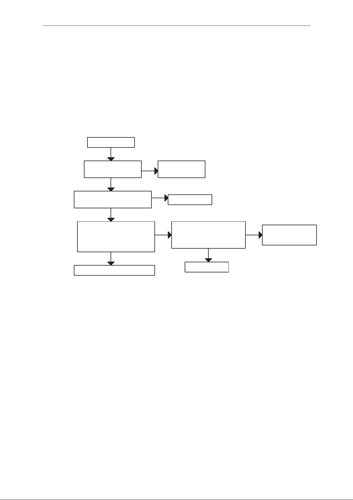
Phone is totally dead
This means that phone doesn’t draw current at all when the power switch
is pressed or when the watchdog disable is grounded (J113, J114 connected together).
Used battery voltage must be higher than 3.0 V. Otherwise the hardware
of CCONT (N100) prevents totally to switch power on.
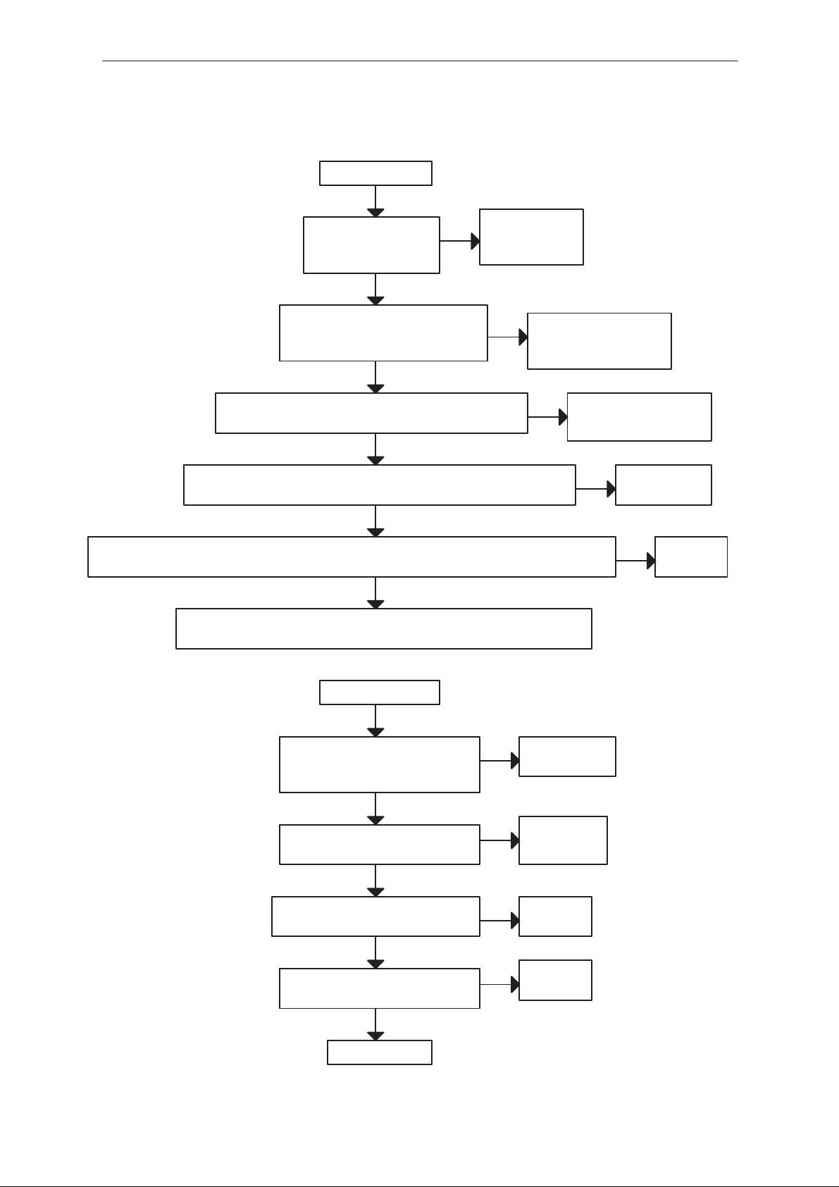
Phone is totally dead
YES
Check VBATT at CCONT
(N100 pins 8,12,...) =3.6V
YES
Voltage at pin 29 of CCONT (N100)
is 3.6 V
Technical Documentation
NO Failure in VBAT line
Check X101, X102
NO
Faulty circuit N100
YES
N100 pin 55 (VBB) 2.8 V
N100 pin 25 (VXO) 2.8 V
when PWR switch is pressed
or watchdog disable pin is grounded
YES
See section: Power Doesn’t Stay On
NO
CCONT (N100) pin 29 0V when
PWR switch is pressed or
watchdog disable is grounded
Faulty circuit N100
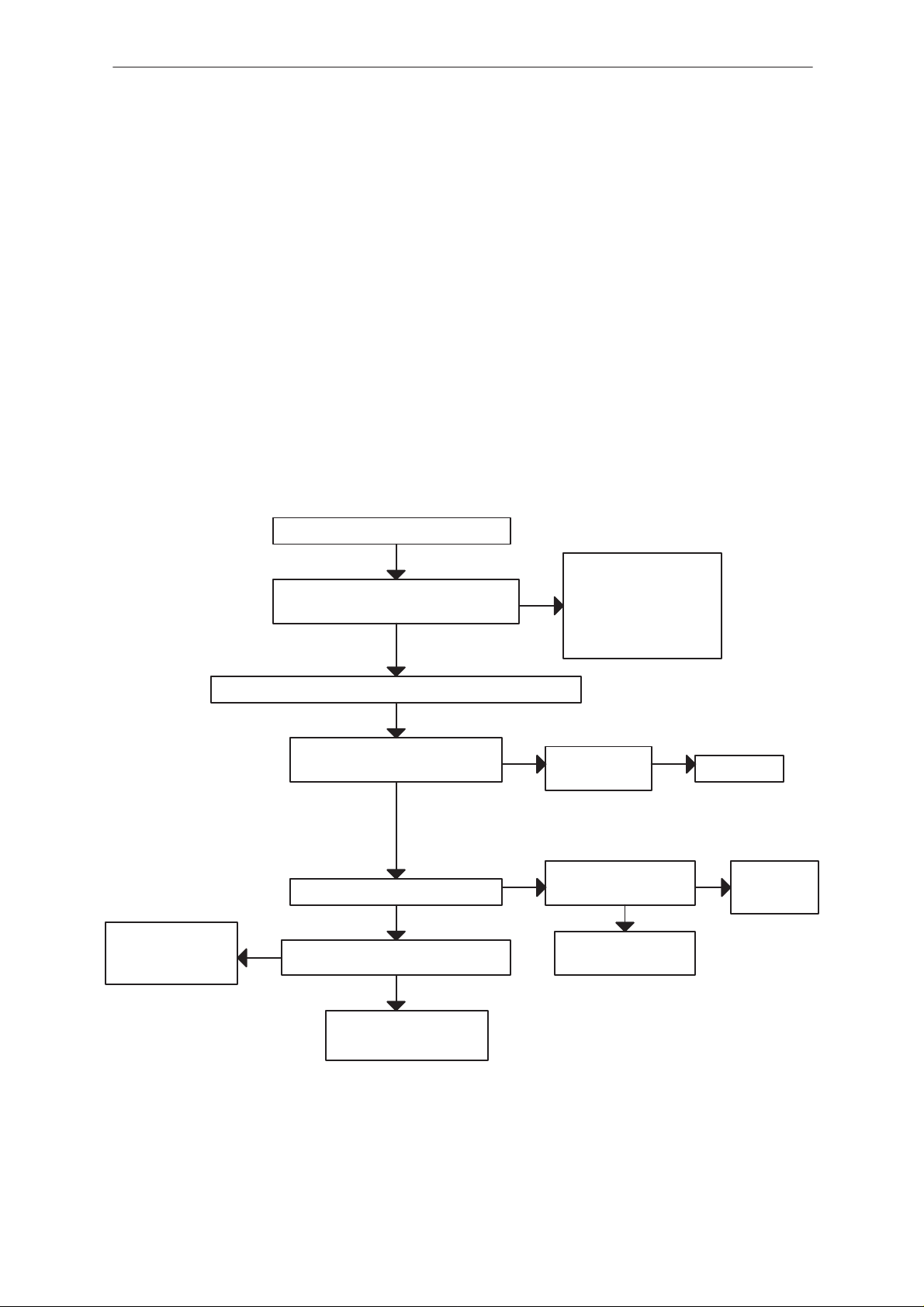
Flash programming doesn’t work
There is two possibilities to route programming voltage VPP.
– If regulator N200 is used the programming voltage comes from the regulator (VPPSW) via UI–connector to flash memory D210.
– Other way is to route Vpp from CCONT pin 36 to UI–connector and
again to flash memory.
NO Check X99,R103
Check UI module
YES
Page 4
In flash programming error cases the flash prommer can give some information about a fault.
The fault information messages could be:
– MCU doesn’t boot
– Serial clock line failure
– Serial data line failure
– External RAM fault
– Algorithm file or alias ID don’t find
– MCU flash Vpp error
Original 05/98
Page 5
PAMS
NSK–1/3
Technical Documentation
In cases that the flash programming doesn’t succeed it is possible to
check short circuits between the memories and the MCU (MAD2). This
test is recommended, when the fault information is: MCU doesn’t boot,
Serial clock line failure or Serial data line failure.
The test procedure is following:
1. Connect the short circuit wire between the test points J206 and J207.
2. Switch power on
3. If the voltage level in testpoint J205 is 2.8 V (”1”), the interface is OK. If
there is a short circuit, the voltage level in testpoint J205 stays low and
32kHz square wave signal can be seen in the lines which are already
tested.
It must be remembered that this test can only be used to find short circuits, not open pins. Also upper data lines (15:8) of flash circuit D210 are
not included to this test.
Troubleshooting Instructions
passed
CCONT pin 54
MAD pin 38
MAD pin 134
J225
( PURX )
( MCUAD0)
( ExtSysResX))selftest
Original 05/98
Page 5
Page 6
NSK–1/3
PAMS
Troubleshooting Instructions
Flash Programming (1)
Flash programming doesn’t work
If the fault information from the prommer is:
connect watchdog disable (J114) to GND (J113)
EEPROM (D230) pin8 (VBB) 2.8V
VVCXO 2.8V (G703, C721)
YES
a) MCU doesn’t boot
b) serial data line failure
c) serial clock line failure
connect:
OK
YES
NO
Technical Documentation
check
WDDIS line –> N100 pin29
OK
Check
Fault finding chart
for 13 MHz
oscillator
See section: Phone is totally dead
NO Sleep clock (SCLK) J201
J121 (Purx)=”1” (2.8V)
YES
NO
MAD2 pin 93 (J200): 13MHz sine wave
clock signal: 500 mVpp min.
YES
Check that following lines are correct from X131 to D200:
MBUS: X131 pin11 –> D200 pin112
FBUS_TX: X131 pin13 –> D200 pin104
FBUS_RX: X131 pin12 –> D200 pin109
check also pullup and pulldown resistors: R200, R201, R123
GND : X131 pin 9 –> GND
OK
Enable the selftest function of D200 by connecting
shortcircuit between testpoints J206 and J207
Connect an oscilloscope to testpoint J205 and switch
power on
square wave 32 kHz
Faulty circuit N100
or over loaded PurX line
YES
check sleep
NO
clock circuitry
(B150,R197...)
Page 6
Voltage level rises to ”1” after power on at testpoint J205
YES
There could be open pins in circuits D200 (D211, D240)
If not, the PCB or D200 (D221, D210) is faulty
NO
There is a shortcircuit
somewhere in memory control
lines or MCU address lines or
MCU lower (7:0) data lines
Original 05/98
Page 7
PAMS
NSK–1/3
Technical Documentation
Flash Programming failure (2)
Flash progrmming doesn’t work
YES
If the fault information from the prommer is:
External RAM fault
YES
Check pins of SRAM (D221)
Check control lines of SRAM:
RAMSelX ...
Troubleshooting Instructions
Flash progrmming doesn’t work
YES
If the fault information from the prommer is:
Algorithm file or alias ID don’t find, ID is unknown etc.
YES
Flash progrmming doesn’t work
YES
If the fault information from the prommer is:
MCU flash Vpp error
YES
D210 pin13 (C211)
Vpp=2.8V
YES
Faulty component
D210 or C211
NO
Check output of regulator
N200 pin4 2.8V
YES
Check UI connector X99
and zero ohm resistor
Check pins of FLASH (D210)
Check control lines and upper data lines (15:8)
of FLASH: ROM1SelX...
NO
Check V8
N200 pin6
Faulty component N200
or C213, C212
NO
Check V109,
C124, C148
Faulty
component
N100
Original 05/98
Page 7
Page 8
NSK–1/3
PAMS
Troubleshooting Instructions
Technical Documentation
Power doesn’t stay on, or phone is jammed
If this kind of fault has come after flash programming, there are most
probably open pins in ICs.
The soldered joints of ICs: D200 (MAD2), D210 (FLASH), N100
(CCONT), D221 (SRAM) are useful to check at first.
Normally the power will be switched of by CCONT (N100) after 30 seconds, if the watchdog of the CCONT can not be served by software.
The watchdog updating can be seen by oscilloscope at pin 50 (DataselX)
of CCONT.
In normal case there is a short pulse from ”1” –> 0 every 8 seconds.
The power off function of CCONT can be prevented by connecting a short
circuit wire from CCONT pin 29 to ground.
Power doesn’t stay on or phone is jammed
Check:
Fault finding chart for
13MHz oscillator
YES
CCONT watchdog is served?
(pin 50 pulses 1 –> 0)
NO
Connect watchdog (WWDDIS) to GND (J113,J114)
OK
EEPROM (D230) pin8 (VBB) 2.8V
VVCXO 2.8V (CCONT pin25 –> G703)
YES
J121 (PURX) = ”1” (2.8V)
YES
NO
MAD2 (D200) pin 93: 13 MHz sine wave
clock signal: 500 mVpp min.
YES
NO
NO J201 sleepclk (SLCLK)
software is able to run
YES
check UI module
If power is switched off
after few seconds, check
BSI and BTEMP lines
VBAT is correct
3.6 V
square wave 32 kHz
Faulty circuit N100
or over loaded PurX line
YES
YES
N100 is faulty
check sleep
NO
clock circuitry
(B150, R197...)
Page 8
Open pins or faulty circuit:
D200, D210, D221, N100
Original 05/98
Page 9

PAMS
NSK–1/3
Technical Documentation
Troubleshooting Instructions
Display Information: Contact Service
This fault means that software is able to run and thus the watchog of
CCONT (N100) can be served.
Selftest functions are run when power is switched on and software is
started to excute from flash.
If any of selftests is failed, contact service information will be shown on
display.
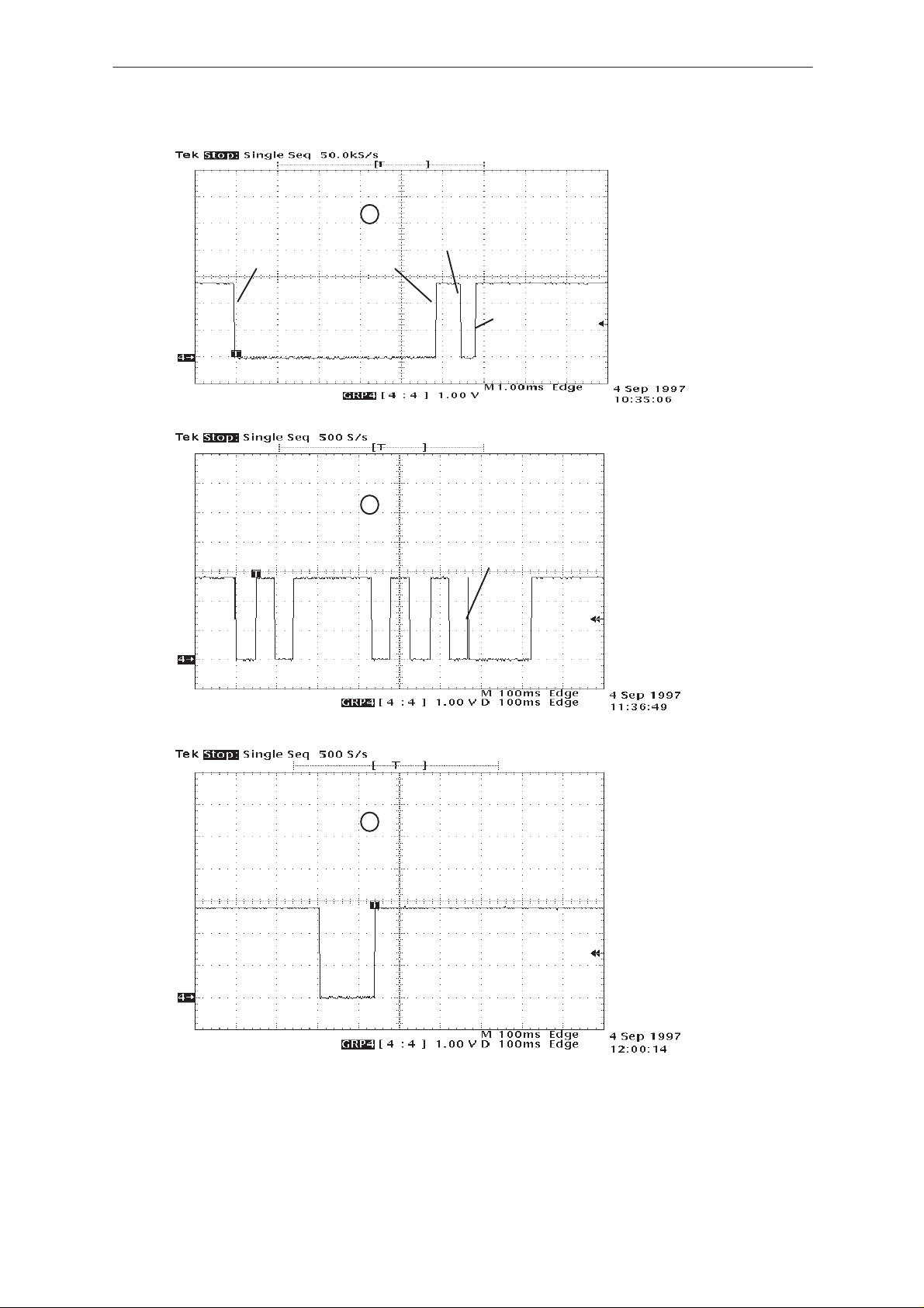
The phone doesn’t register to the network or phone
doesn’t make a call
If the phone doesn’t register to the network or the phone doesn’t make a
call, the reason could be either the baseband or the RF part.
The phone can be set to wanted mode by WinTesla service software and
determinate if the fault is in RF or in baseband part (RF interface measurements).
The control lines for RF part are supplied both the System Asic
(MAD2;D200) and the RFI (Cobba; N300). MAD2 handles digital control
lines ( like synthe, TxP etc.) and Cobba handles analog control lines (like
AFC, TxC etc.).
The DSP software is constructed so that operation states of DSP (MAD2)
can be seen in external flag (DSPXF) output pin (D200 pin 91).
After power up, DSP signals all completed functions by changing the state
of the XF pin (see figures 39 and 40).
1. DSP initialization done
2.Synchronization to network
done
3. Registrarition to network
done.
1 2 3
Original 05/98
MAD2 pin 91 (DSPXF)
J222
Page 9
Page 10
NSK–1/3
PAMS
Troubleshooting Instructions
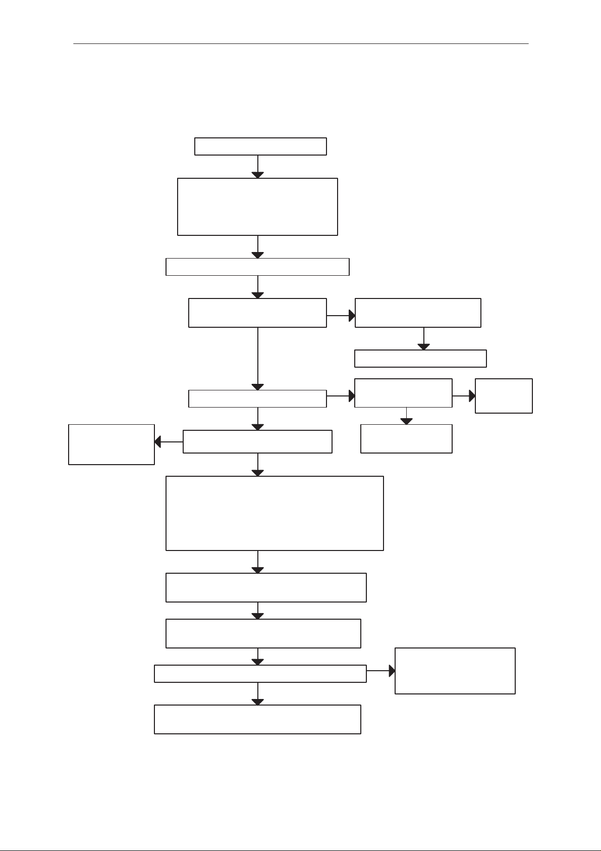
init
initialize
1
patch code
download
2
dsp
constants
download
initialization
done
Technical Documentation
MAD2 pin 91 (DSPXF)
J222
channel
scan starts
PSW
search last PSW
OK
3
send RACH
RACH OK
go SDCCH
imediate assigment
OK
synchronization
OK
MAD2 pin 91 (DSPXF)
J222
MAD2 pin 91 (DSPXF)
J222
Page 10
Original 05/98
Page 11

PAMS
NSK–1/3
Technical Documentation
Phone register failure
Phone doesn’t register to the network
phone doesn,t make a call
Analog supply voltage VCOBBA is 2.7 V
at pin 7,12 ... of Cobba (N300)
Analog reference voltage Vref is 1.5 V
at pin 9 of Cobba (N300)
Supply voltage VCP (N100 pin 32) > 4.8 V
Supply voltage VRX (N100 pin 11) > 2.7 V
Supply voltage VSYN_A (N100 pin 15) > 2.7 V
Supply voltage VSYN_D (N100 pin 4) > 2.7 V
during the receiving slot
Supply voltage VTX (N100 pin 20) > 2.7 V
during the transmitting slot
or
YES
YES
YES
Troubleshooting Instructions
Check
NO
N100
NO
Check
R270, R271
NO Check
N100, D200
YES
Synthesizer lines: SEna (N401 pin 56),
SClk (N401 pin 54)
SData (N401 pin 55)
pulses 0 –> 1 during receiving slot
YES
NO
Check
D200
RF control lines: AGC (N300 pin 18) 0 –> 2.3 Vmax during receiving slot
AFC (N300 pin 19) 0 – 1.2 V typ. during receiving slot
YES
Analog data signal RxIP (N300 pin 22) 0–> 1.5 V DC during receiving slot
Analog data signal RxIN (N300 pin 23) 0–> 1.5 V DC during receiving slot
Used benefit signal is biased to DC and its amplitude is 50 mVpp
nominal and frequency is 13 MHz
YES
NO
DAX signal (N300 pin 48) pulses 1 –> 0 during receiving slot
YES
RF control lines: TxC (N300 pin 17) 0 –> 2.3 Vmax during transmit slot
TxP (D200 pin 176) 0–>1 (2.8 V) during transmit slot
YES
NO
Check
N300
NO
Check
N300 if DC is failed
Check
RF part if benefit signal is failed
Check
N300
Check
NO
N300 if TxC is failed
Check
D200 if TxP is failed
Analog data signals: TxIN (N300 pin 13) 0–> 0.8 V DC during transmit slot
Used benefit signal is biased to DC and its amplitude is 300 mVpp
Original 05/98
TxIP (N300 pin 14) 0 –>0.8 V DC during transmit slot
TxQN (N300 pin 15) 0 –>0.8 V DC during transmit slot
TxQP (N300 pin 16) 0 –>0.8 V DC during transmit slot
nominal and frequency is 64 kHz
NO
YES
Check
N300
Check
RF part
Page 11
Page 12
NSK–1/3
PAMS
Troubleshooting Instructions
Instructions for RX troubleshooting
Apply 1842.5 MHz
–50dBm signal to
external RF–connector
X451.
Check
duplexer(Z401)
(max IL 3dB) output:
P:~53dBm
Check filter Z604
(max IL 3.2) output:
P:–40dBm
N
Check RF–connector
X451. Check input
of duplexer. Replace
if necessary.
N
Check input of Z604
and L611.
P:–37dBm
NN
Check input of
C601:
P:–37dBm
Technical Documentation
Check C600,R611
and measure CRFU
pin 5:2.4V
Check C603 and
C604. Check CRFU
pin 18 and 19:
f:487MHz P:–24dBm
N
CRFU pin 21:2.7V
pin 23:P:–40dBm
Change
filter Z604.
pin 14:2.8V
Check R612
and CRFU pin
12:1.2V
Check V600;
b:0.86V.
Check C623 and
L610
Check CRFU
pin 4:2.8V
(FRAC)
Check R600 and
C666: 2.7V
N
Goto BB
troublesh.
N
Goto BB
troublesh.
Page 12
CRFU pin 16:
(MID ch) P:–4dBm
N
Check C710.
Goto UHF VCO
troublesh.
Original 05/98
Page 13
PAMS
NSK–1/3
Technical Documentation
CRFU pin 25 and 26:
f:487MHz P:–36dBm
N
CRFU pin 2 and 3:
f:87MHz P:–17dBm
Check output of filter
Z605 pin 6 and 9:
f:87MHz P:–26dBm
N
N
Check filter Z621
(max IL 4.5dB)
Check
L601,L602,C609
and C611: V :2.7V
(VRX)
CRFU pin 1:2.7V
CRFU pin 28:
f:400MHz P:–14dBm
Check input of
Z605: –17dBm
Troubleshooting Instructions
N
Change
Z621
N
Goto BB
troublesh.
N
Check VHF VCO
troublesh.
N
Check L703,C718
and C719
Check PLUSSA pin
64: f:400MHz
P:–12dBm
N
Check C612 and
C613
N
Check VHF VCO
troublesh.
Check R604 and
PLUSSA pin 44
from J413:
f:13MHz P:+3dBm
Check output of filter
Z606 from J412:
f:13MHz P:0dBm
Check J410 (RXN)
and J411 (RXP):
f:13MHz V:0.9V
PLUSSA pin 51
N
and 52: f:87MHz
P:–26dBm
Check AGC–signal
from J406:start of
pulse 1.1V and
center:
MID ch 1.3V
Check C618 and
PLUSSA pin 47:
2.7V (VRX)
N
Change
filter Z606
N
Check C641
and C640
Check
C602,C614,L608
and L609: 2.7V
(VRX)
N
NN
N
Check
R603,C617,C616
and L607
Check C624
and R610
Goto BB
troublesh.
N
Check BB
troublesh.
Goto BB
troublesh.
Original 05/98
Check PLUSSA
pin 29 and 30:
f:13MHz V:1.8V
N
PLUSSA pin 34
and 35: f:13MHz
Pin 34: –10dBm
Pin 35: –5 dBm
Check PLUSSA pin
47: 2.7V
pin 17 and 28: 4.7V
N
Check
C620,R606
and R605
Page 13
Page 14

NSK–1/3
PAMS
Troubleshooting Instructions
Instructions for TX troubleshooting
N
TXQP:R501 0.8V
TXQN:R501 0.8V
TXIN:R504 0.8V
TXIP:R504 0.8V
N
TXP:J408 >2 V
TXC:J407 0.5–2 V
depending on
TX–level
N
Check PLUSSA
N401 pin 61 and 62:
f:400MHz
P:–19...–15dBm
Goto Baseband
(BB)
troubleshooting
Goto
BB
troublesh.
Check PLUSSA pins
2, 10 and 63:
2.8V (VTX)
pin 58: 1.5V (VREF)
Technical Documentation
N
Goto BB
troublesh.
CRFU (N402)
pin 7 and 9: f:400MHz
P:–19...–15dBm
Check CRFU (N402) pin
11: MID ch
P:–3...+5dBm
N
PLUSSA (N401)
pin 8:
f:800MHz
P:–2dBm
Change
PLUSSA
N
Check C527, C545,
L501, L500, C519
and C518
NN
CRFU (N402)
pin 13:2.8V
N
CRFU pin 16:
f: MID ch +1dBm
Check CRFU pin
14:2.8V
Goto VHF VCO
troublesh.
Goto BB
troublesh.
Goto UHF VCO troublesh.
Page 14
Change
CRFU
Original 05/98
Page 15

PAMS
NSK–1/3
Technical Documentation
Check filter Z503
output from C561:
P:–7...+4dBm
f:MID ch
Check PA pin 6:
f: MID ch
P:+3...+8dBm
Check input of
duplexer (Z401):
P:3–33dBm
TX–level:15–0
N
Check IL of
Z503
max 4.2 dB
N
Check IL of filter Z505
Check TX buffer
c:2.4V b:0.9V
N
Check control
signal from J404:
V:1–2.8V
TX–level:15–0
N
max 3.5 dB
V510:
Change
Z503
N
N
Check VTX 2.8V
pulse from R571
N
TXP:J408 2.8 V
TXC:J407 0.5–2 V
Check
PLUSSA
pin 12:0.5–1.8V
pin 15: 2.8V
Troubleshooting Instructions
Change Z505
N
Goto BB
troublesh.
N
Goto BB
troublesh.
Check signal from
antenna pad J400
and RF–connector
X451
Check PA (N500)
pin 9: same as J404
pin 2 and 8: VBAT
pin 12 and 13:VBAT
Change
PA
N
No signal to X451 >
PCB is bad
No signal to J400 >
X451 is bad
Check V504;
c:VBAT b:1.7–3.8V
Check N501 pin 3:
(V5V) 5V
N
Check input
of Z511:
VBAT
Change
Z511
N
Check N501 pin 1:
0V during TXP
pin 4: 5V but during
TX burst ~4V
N
Goto BB
troublesh.
N
Check voltage from
Change N501
POWER DETECTION:
Check TXL–signal from base of V509:
TX–level:
0–7: b:0.1V > c:4...5V
8–15: during burst b:2.8V > c:0V
Check J403:
TX–level:
0–7:30...80mV during burst
8–15:1.4...1.8V during burst
between bursts 0.3V
C509: 5V
N
N
N
Goto BB
troublesh.
Goto BB
troublesh.
Change V501
Original 05/98
Page 15
Page 16

NSK–1/3
PAMS
Troubleshooting Instructions
Fault finding chart for 13 MHz oscillator
PLUSSA pin21:
13MHz
Vpp:0.6V
Check
AFC–signal from
C720:1.1V
Check
RFCLK–signal from
L701: f:13MHz
P:5dBm Vpp:0.84V
N
Check AFC–signal
from R714 and
C720:1.1V. Check
VVCXO–signal from
C721:2.8V.
N
Goto BB
troublesh.
N
Check C722. Check V710;
c:13MHz Vdc:0.95V Vpp:0.8V
b:13MHz Vdc:0.6V Vpp:0.1V
N
Goto BB
troublesh.
Technical Documentation
N
Check R717 and C721:2.8V
Check R707,R706 and C760
Check PLUSSA (N401)
pin 54 (SCLK):2.8V
pin 55 (SDA TA):2.8V
pin 56 (SENA):2.8V
SENA is 0 during SCLK
and SDA TA
N
Goto BB
troublesh.
Page 16
Original 05/98
Page 17

PAMS
NSK–1/3
Technical Documentation
Fault finding chart for VHF VCO
N
PLUSSA pin 8:
800MHz
P:0dBm
Check
C709
N
Check
VSYN_A–signal
from R708:2.8V
Check R708,C714
and C716.
N
PLUSSA pin 18
(PD):2.2V
SENA is 0 during SCLK
Troubleshooting Instructions
Goto BB
troublesh.
Check PLUSSA (N401)
pin 54 (SCLK):2.8V
pin 55 (SDA TA):2.8V
pin 56 (SENA):2.8V
and SDA TA
N
Goto BB
troublesh.
Check
C707,R712,R729.
Voltage in R729:
2.25V
PLUSSA pin
9,22 and
25:2.75V
Change
module G702
N
Signal VSYN_D
troublesh.:Check
R715,R716,C7
28 and C735
Change
PLUSSA
R715 and
R716:2.8V
Check
N
Goto BB
troublesh.
Original 05/98
Page 17
Page 18

NSK–1/3
PAMS
Troubleshooting Instructions
Fault finding chart for UHF VCO
PLUSSA pin 24:
RX:f:1318.2–1392.8MHz
P:0dBm
TX:1310.2–1384.8MHz
P:–1dBm
CRFU2a pin 1
and 14:2.8V
N
Check C775
and C710
Check CRFU2a
pin 16: Same as
PLUSSA pin 24!
P:0dBm
Check
C774,R760,R758,
C773 and R759.
Check V720:
c:2.6V
N
VSYN_A
missing. Goto
BB troublesh.
N
CRFU2a pin
1 and
14:2.8V
N
Check
C671,C704,C761
and C706
Technical Documentation
N
Goto BB
troublesh.
Check connection
of R701 and
C700:2.7V
Check control signal
from R703:
RX:1.4–3.4V
TX:1.2–3.2V
This is also visible at
PLUSSA pin 27.
Change
module
G701
N
R702,R703,R704,
C703 and C702.
Check
Page 18
Original 05/98
Page 19

PAMS
NSK–1/3
Technical Documentation
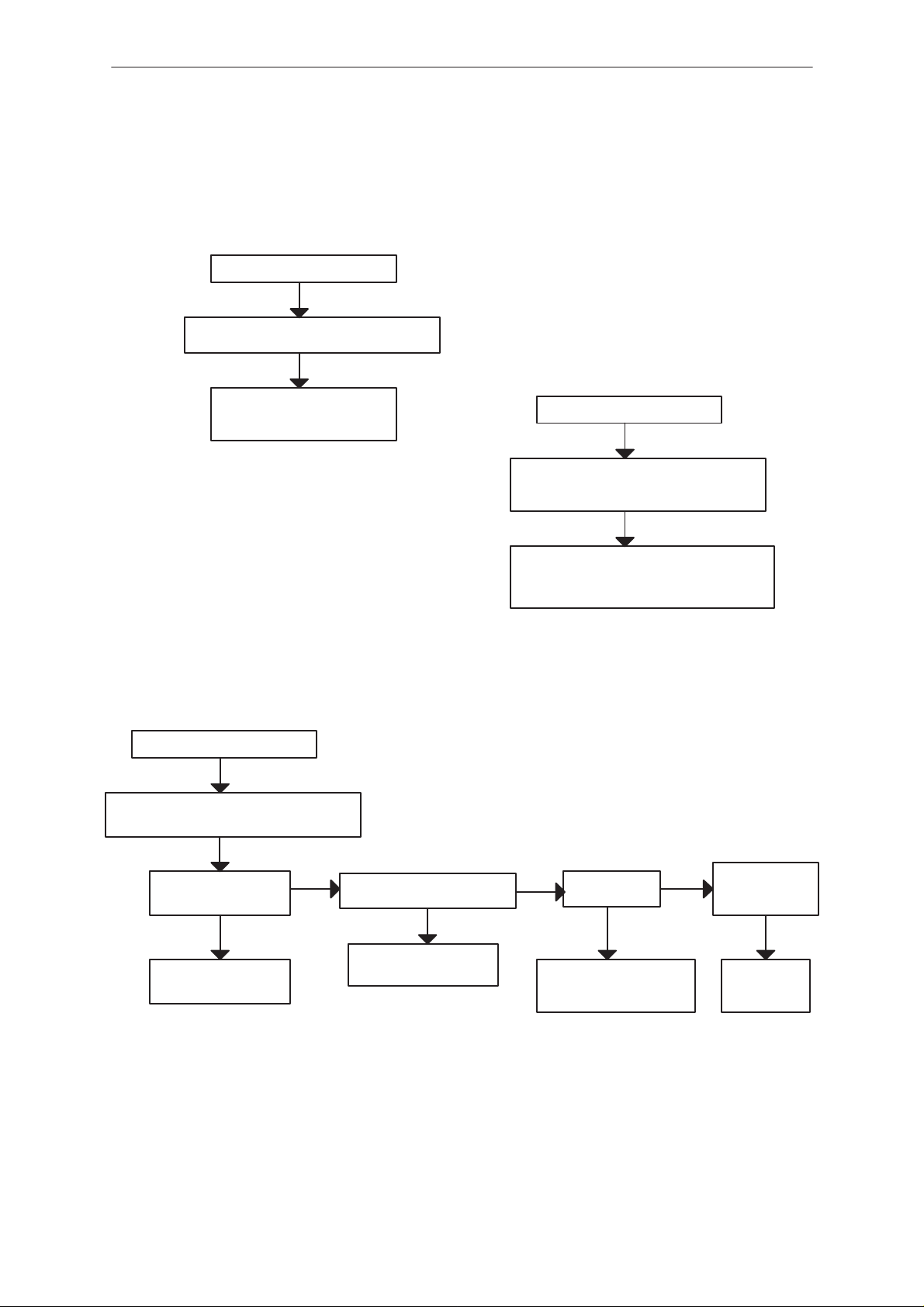
SIM card is out of order
The hardware of the SIM interface from MAD2 (D200) to the SIM connector (X150) can be tested without SIM card.
When the power is switched on and if the BSI line (X101;1) is grounded
by resistor, all the used lines (VSIM, RST, CLK, DATA) rises up four times.
Thus ”Insert SIM card” faults can be found without SIM card.
The fault information ”Card rejected” means that ATR message (the first
message is always sent from card to phone) is sent from card to phone
but the message is somehow corrupted, data signal levels are wrong etc.
or factory set values (stored to the EEPROM) are not correct.
Troubleshooting Instructions
Original 05/98
Page 19
Page 20
NSK–1/3
PAMS
Troubleshooting Instructions
SIM Card failure
VSIM, DATA, RESET and CLOCK lines
at Sim–card reader (X150) rises up to 5V
after power on
VSIM Outputs (pins 36,38,42,43) at CCONT (N100)
VSIM Inputs (pins 30,39,40,41,44) at CCONT (N100)
rises up to 2.8 V after power on
Insert SIM card fault
YES
Voltage level < 1.5 V
at pin 95 of D200 when
BSI resistor is connected
YES
NO
rises up to 5 V after power on
NO
NO
NO
Technical Documentation
Check
R107,R104,X101
C120, C121
YES
Check
SIM card and SIM reader
connectors
YES
Check
X150,R152,R101,
C108,C106,C107,C167
YES
faulty circuit
N100 (CCONT)
VSIM –lines (pins 129,120,127,126,128) at MAD2 (D200)
rises up to 2.8 V after power on
NO
Check again that voltage level at pin 95 (SIMCardDetX) of D200 is lower than 1.5V
If it is, change D200
Card Rejected fault
YES
VSIM is according the specification
VSIM = 2.8 V min (with 3 V SIM card)
NO
faulty circuit
N100 (CCONT)
VSIM = 4.5 V min (with 5 V SIM card)
YES
The ATR data can be seen at pin 43
(CCONT, N100)
YES
The ATR data can be seen at pin 120
(MAD2, D200)
YES
SIMIOControl line (N100 pin 36) is ”1”
during the ATR message
NO
NO
NO
Check
X150,R101
Check
N100
Check
D200
YES
faulty PCB
Page 20
YES
Check D200
Original 05/98
Page 21

PAMS
NSK–1/3
Technical Documentation
Audio failure (1)
Troubleshooting Instructions
Uplink (microphone) and downlink (earphone) are broken
YES
Voltage at pin 107 of MAD2 (D200)
is 2.8 V (without external audio devices) HOOKDET
YES
Voltage at pin 108 of MAD2 (D200)
is 2.8 V (without external audio devices) HEADDET
YES
Frequency at pin 138 of MAD2 (D200)
is 1 MHz, square wave 2.8 Vpp
YES
NO
NO
NO
Check
R130,R155,
R300,C300
Check
R154,R301,,R302,
R300,R332,
C306,C308
Check
N300 (Cobba)
Frequency at pin 139 of MAD2 (D200)
is 8 kHz, square wave pulses 2.8 Vpp
Uplink (microphone) is broken
YES
Voltage at pin 6 of X131 is 1.8V
NO
Voltage at pin 7 of X131 is 0.3V
during a call
YES
DC voltage at pins 59 and 60 of
NO
N300 is 1.4 V during a call
YES
Analog audio signal (few millivolts) at pins 59 and 60
of N300 during a call
YES
Digital PCM data at pin 137 of MAD2 (D200)
during a call
Check
N300 (Cobba)
NO
NO
Check
N300 (Cobba)
Check
microphone
Check X131 and micbias
components: V300,R335...
Check
C336, C335 and PCB
routings
NO
ok
Check
N300 (Cobba)
Original 05/98
Page 21
Page 22

NSK–1/3
PAMS
Troubleshooting Instructions
Audio failure (2)
Downlink (earphone) is broken
YES
Digital PCM data at pin 52 of Cobba (N300)
during a call
YES
DC voltage at pins 5 and 6 of
N300 is 1.4 V during a call
YES
Analog audio signal (some ten millivolts) at pins 5 and
6 of N300 during a call
NO
NO
N300 (Cobba)
Check
D200 (MAD2)
Check
NO Check
Technical Documentation
N300 (Cobba)
Page 22
Original 05/98
Page 23

PAMS
NSK–1/3
Technical Documentation
Charger failure
Nothing happens when charger is connected
Voltage level at pin 60 of CCONT (N100)
is higher than 0.4 V when charger is connected
Display Information: Not charging
YES
YES
Check N100
YES
Troubleshooting Instructions
NO
Check
X131, F100, L109
R127,R134,R146,
C140
Voltage level at pin 62 of CCONT (N100)
is about 0.8 V (BSI –resistor 39K) when
power is connected
Depends about BSI resistor value
Voltage level at pin 63 of CCONT (N100)
is about 0.5 V when power is connected
BTEMP resistor value should be 47 k
32 Hz square wave frequency at pin 7 of CHAPS (N110)
Voltage levels at pins 5 and 12 of CHAPS (N110)
are same as VBAT
Voltage levels at pins 5 and 12 of CHAPS (N110)
rises when charger is connected
YES
YES
YES
YES
NO
NO Check
NO
NO
NO
Check
X101, R107
X101, R107
Check
N100
Check
R109, N110
Check
N110
Original 05/98
Page 23
Page 24

NSK–1/3
PAMS
Troubleshooting Instructions
Technical Documentation
This page intentionally left blank.
Page 24
Original 05/98
 Loading...