

Page 1

CC Technical Documentation
NPM-10 (3595) Series Transceivers
Troubleshooting - RF
Issue 2 03/2004 Confidential ©2004 Nokia Corporation
Page 2

NPM-10 (3595)
Troubleshooting - RF CC Technical Documentation
Contents Page
RF Troubleshooting ....................................................................................................... 3
Abbreviations in Troubleshooting Charts ....................................................................3
Introduction ..................................................................................................................3
General Description of the RF Circuits .......................................................................4
Receiver Signal Path ................................................................................................. 4
Transmitter Signal Path............................................................................................. 5
PLL............................................................................................................................ 5
Key RF Component Placement................................................................................. 7
Power Supply Configuration..................................................................................... 8
Receiver .....................................................................................................................10
General Instructions for GSM 850 Rx Troubleshooting......................................... 10
Troubleshooting Chart for the GSM 850 Receiver................................................. 12
General Instructions for GSM 1900 Rx Troubleshooting....................................... 13
Troubleshooting Chart for PCS Receiver................................................................ 15
Measurement Points in the Receiver....................................................................... 17
Transmitter .................................................................................................................18
Measurement Points for the Transmitter................................................................. 18
General Instructions for GSM Tx Troubleshooting................................................ 19
Troubleshooting Chart for GSM 850 Transmitter................................................... 21
General instructions for PCS Tx troubleshooting................................................... 23
Synthesizer .................................................................................................................26
General Instructions for Synthesizer Troubleshooting............................................ 26
26 MHz Reference Oscillator (VCXO)................................................................... 27
VCO ........................................................................................................................ 28
Troubleshooting Chart for PLL Synthesizer.......................................................... 28
Measurement Points for the PLL ............................................................................ 31
Frequency Lists....................................................................................................... 33
Alignment ..................................................................................................................35
NPM-10 (3595) Manual Align with Phoenix.......................................................... 35
Rx Calibration......................................................................................................... 36
Rx Channel Select Filter ......................................................................................... 39
Rx Band Filter Response......................................................................................... 40
Tx Tuning ..................................................................................................................42
Tx Power Tuning GSM 850.................................................................................... 42
Tx Power Tuning PCS 1900.................................................................................... 44
Tx I/Q Tuning ............................................................................................................44
RF Control .................................................................................................................48
Call Testing ................................................................................................................48
Page 2 ©2004 Nokia Corporation Confidential Issue 2 03/2004
Page 3
NPM-10 (3595)
CC Technical Documentation Troubleshooting - RF
RF Troubleshooting
Abbreviations in Troubleshooting Charts
Table 1: Troubleshooting Abbreviations
Abbreviation Definition
BB Base band
DC Direct current
ESD Electrostatic discharge
FEM Front End Module
LF Low frequency
LO Local oscillator
LPF Low pass filter
Introduction
Two types of measurements are used in this chapter. It will be specified if the measurement type is RF or LF.
• Use a spectrum analyzer with a high impedance probe for RF measurements.
PA Power amplifier
PLL Phase-locked loop
PWB Printed wiring board
RCT Radio communication tester
RF Radio Frequency
Rx Receiver
Tx Transmitter
UHF Ultra-high frequency
VCO Voltage-controlled oscillator
Also, it is recommended that you use a good phone as a benchmark for the
measurement technique because signal levels can vary depending on the
measurement setup. Measurements stated in this section were done with an
HP85024 high-impedance probe.
Note: The test jigs have some losses which must be taken into consideration when calibrating
the test system.
• Use a 10:1 probe and an oscilloscope to measure the LF (low frequency) and DC
(direct current). The probe used in this chapter is an 10MΩ/8pF passive probe.
If using another probe, keep in mind that the voltages displayed may be slightly
different.
Issue 2 03/2004 ©2004 Nokia Corporation Confidential Page 3
Page 4
NPM-10 (3595)
Troubleshooting - RF CC Technical Documentation
Always make sure the measurement set-up is calibrated when measuring RF parameters
on the antenna pad. Remember to include the loss in the module test jig when realigning
the phone.
Most RF semiconductors are static-discharge sensitive. Use ESD protection during
repair (ground straps and ESD soldering irons). Mjoelner is moisture-sensitive, so parts
must be pre-baked prior to soldering.
Apart from key components described in this section, there are a lot of discrete components (resistors, inductors, and capacitors) for which troubleshooting is done by checking
whether the soldering of the component is done properly, and whether the component is
missing from the PWB. Capacitors can be checked for short-circuits and resistors for
value by means of an ohmmeter, but be aware that in-circuit measurements should be
evaluated carefully.
In this chapter, both GSM and GSM 850 will be used for the lower band and both PCS
and GSM 1900 will be used for the upper band.
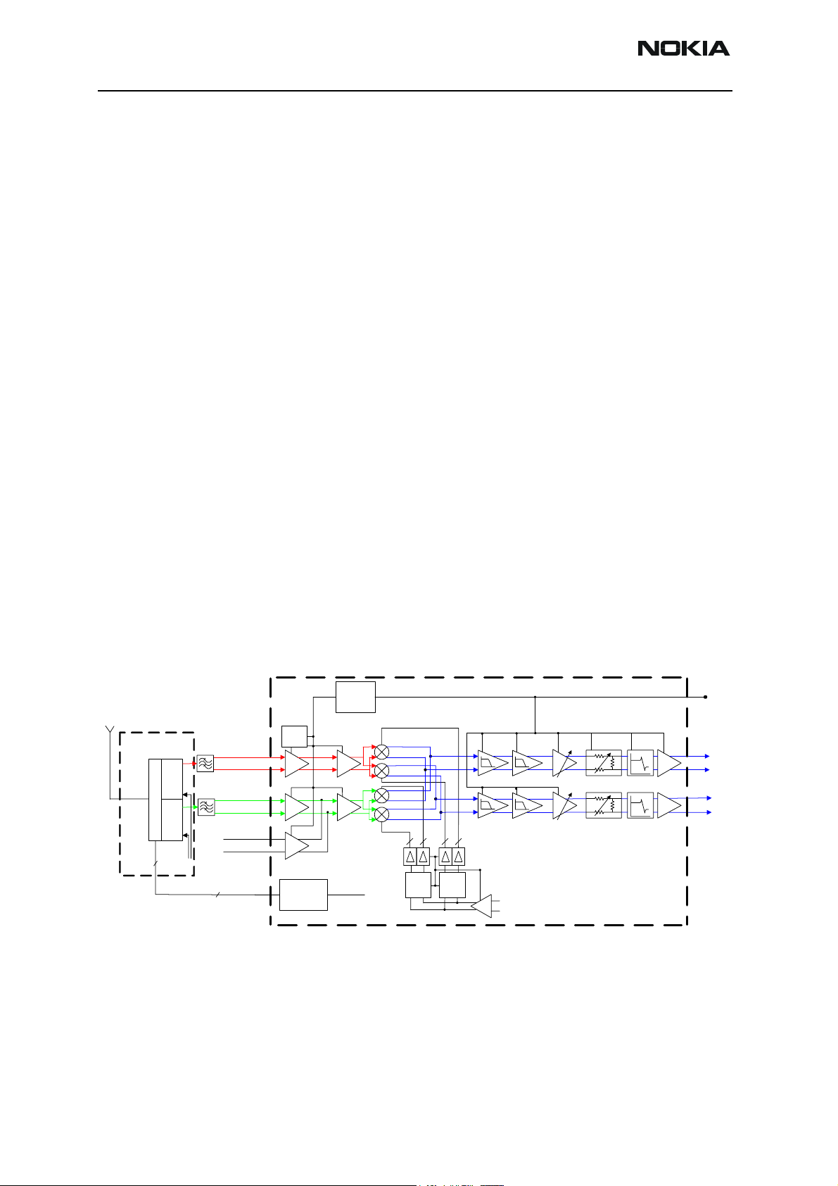
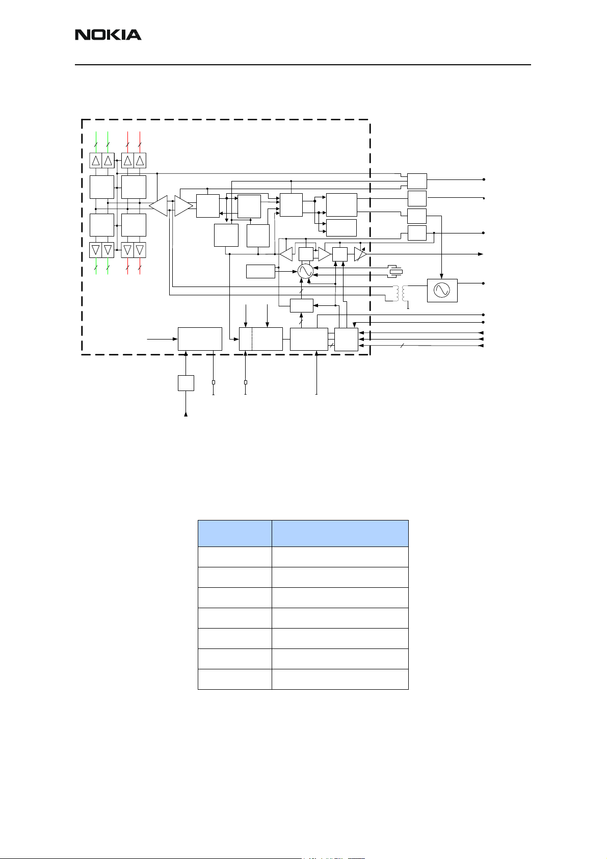
General Description of the RF Circuits
Figure 1 and Figure 2 include different colors in the block diagrams. The GSM 850 signal
route is red, the GSM 1900 route is green, and the common signal lines are blue. Control,
supply voltage, and unused lines are shown in black.
Receiver Signal Path
The signal from the antenna pad is routed to the front end module (N700). The GSM 850
signal passes through the switch inside the FEM to TGSM_Rxout, and the GSM 1900
signal passes through the switch inside the FEM to PCS_Rxout.
R
XSUPPL
FEM
N700
SAW
R
X
GSM
T
X
R
X
PC
SAW
S
T
X
3
VANTL / VANTM/ VANTH
Z60
Z60
LN
A
BIA
L
INP
INM
INP
INM
S
LN
A
L
M
LN
A
M
H
LN
A
H
R
FCONTROL
S
INP
2
RX85
0
INM
RX190
0
1
RX180
0
3
YFILTE
R
X
R
F
D
D
V
PRE
-GAI
N
PRE
-GAI
N
VDDDI
G
VR
X
DCN
DCN
VR
6
RXI
2
P
RXI
M
RXQ
P
RXQ
2
M
B
X
R
B
D
D
V
DCN
LPF
BBAM
P
LPF
BBAM
P
2
222
1/
1/
2
4
1
1
DCN
1
1
AG
C
AG
C
Mjoelner
LPF
LPF
2
BIQUA
D
2BIQUA
D
N600
Figure 1: Receiver signal path
From the FEM PA, the GSM 850 signal is routed to the SAW filter (Z602). The purpose of
the SAW filter is to provide out-of-band blocking immunity and to provide the LNA in
Mjoelner (N600) with a balanced signal. The front end of Mjoelner is divided into an LNA
and a pre-gain amplifier before the mixers.
Page 4 ©2004 Nokia Corporation Confidential Issue 2 03/2004
Page 5
NPM-10 (3595)
CC Technical Documentation Troubleshooting - RF
The output from the mixer is fed to the Mjoelner BB where the signal is amplified in the
BBAMP, and the low pass is filtered in LPF1 before the DC compensation circuits in
DCN1. The DCN1 output is followed by a controlled attenuator and a second low pass
filter (LPF2). The output from LPF2 is DC centered in DCN2 before being fed to the BB for
demodulation.
The GSM 1900 signal chain is similar to GSM 850, but the signal is routed through the
SAW filter (Z601).
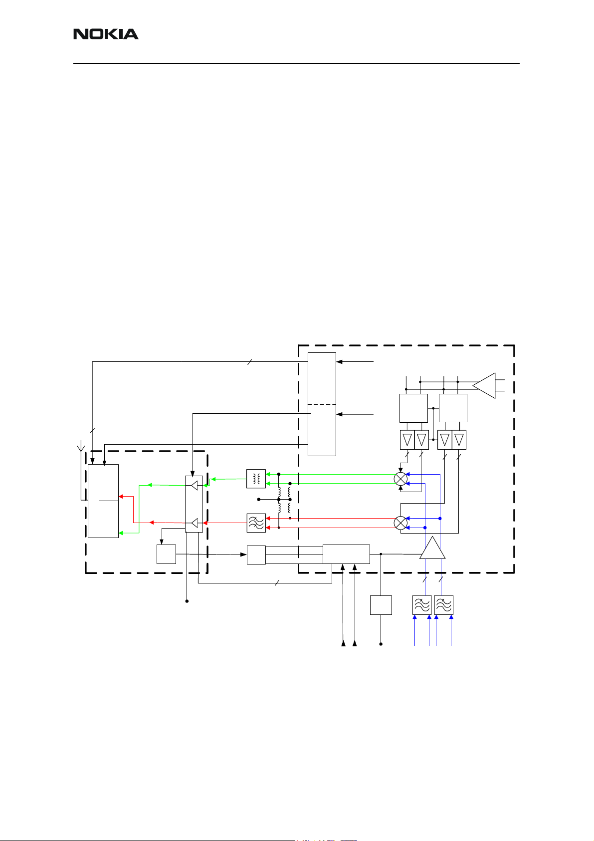
Transmitter Signal Path
The I/Q signal from the BB is routed to the modulators for both 850 MHz and 1900 MHz.
The output of the modulators is either terminated in a SAW filter (Z603) for GSM 850 or
a balun (T602) for GSM 1900. The amplitude’s limited signal is then amplified in the PA
of the FEM (N700). The internal FEM detector, some discrete components, and the
Mjoelner IC (N600) make up the transmitter gain control circuitry. In order to establish
the right Tx output power level, a sample of the signal is taken from the FEM detector
and used in the gain control loop. The Tx signal from the FEM is routed to the antenna,
which depends on the internal switch setting of the FEM.
VANTL / VANTM / VANTH
3
Controls
VTXLOL
3
FEM N700
RX
S
w
GSM
i
t
TX
c
RX
h
PCN
TX
DET
PA
SAW Z603
VBATTRF
Balun
Loop
filter
VTXBH
VTX
PLFB1
PLFB2
2
Controls
OUTHP
OUTHM
OUTLP
OUTLM
DET
VPCH/VPCL
VDDDIG
RF
VDDRXBB
RF
PWC
1/2
2
1/4
2
2
2
Mjoelner
N600
TXP
TXP
TXC
VDDT
Suppl
y
filter
VTX
VR2
X
TXC
2
2
TXIM
TXIP/
TXQM
TXQP/
Figure 2: Transmitter signal path
PLL
The phase-locked loop (PLL) supplies local oscillator (LO) signals for the Rx and Tx mixers.
In order to generate LO frequencies for the required GSM and PCS channels, a regular
synthesizer circuit is used. All PLL blocks (except for the VCO, reference X-tal, and loop
filter) are located in the Mjoelner IC.
Issue 2 03/2004 ©2004 Nokia Corporation Confidential Page 5
Page 6
NPM-10 (3595)
Troubleshooting - RF CC Technical Documentation
The reference frequency is generated by a 26 MHz, voltage-controlled X-tal oscillator
(VCXO), which is located in Mjoelner. Only the X-tal is external. Twenty-six MHz is
supplied to the BB, where a divide-by-2 circuit (located in the UPP IC) generates the BB
clock at 13 MHz. The reference frequency is supplied to the reference divider (RDIV)
where the frequency is divided by 65. The output of RDIV (400 kHz) is used as the
reference clock for the phase detector (ϕ).
The PLL is a feedback control system, which controls the phase and frequency of the LO
signal. Building blocks for the PLL include:
• Phase detector
•Charge pump
• Voltage-controlled oscillator (VCO)
• N-divider
• Loop filter
Note: As mentioned earlier, only the VCO, reference X-tal, and loop filter are external to the
Mjoelner IC.
The VCO (G600) is the component that actually generates the LO frequency. The VCO
generates a differential RF output based on the control voltage input. This signal is fed to
the prescaler and N-divider in Mjoelner. Together, these two blocks divide the frequency
by a ratio based on the selected channel. The divider output is supplied to the phase
detector, which compares the frequency and phase to the 400 kHz reference clock. Based
on this comparison, the phase detector controls the charge pump to either charge or
discharge the capacitors in the loop filter. By charging/discharging the loop filter, the
control voltage to the VCO changes and the LO frequency changes. Therefore, the PLL
keeps the LO frequency locked to the 26 MHz VCXO frequency.
The loop filter consists of the following components: C639-C641 and R618-R619.
The PLL is operating at twice the channel center frequency when transmitting or
receiving in the PCS band. For the GSM band, the PLL is operating at four times the
channel frequency. Therefore, divide-by-2 and divide-by-4 circuits are inserted between
the PLL output and LO inputs to the PCS and GSM mixers.
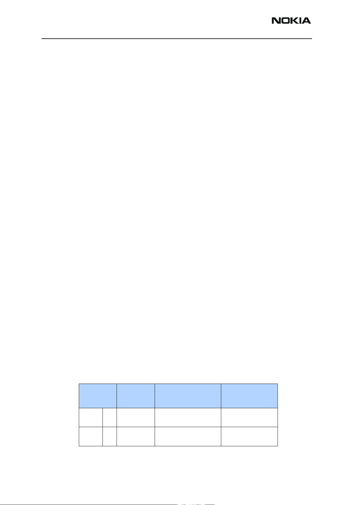
Table 2 shows the PLL frequency plan.
Table 2: PLL Frequency Plan
Frequency
Band
Channel #
System Frequency
Band [MHz]
PLL Frequency
Band [MHz]
GSM RxTx128 - 251 869.2 - 893.8
824.2 - 848.8
PCS RxTx512 - 810 1930.2 - 1989.8
1850.2 - 1909.8
3476.8 - 3575.2
3296.8 - 3395.2
3860.4 - 3979.6
3700.4 - 3819.6
Page 6 ©2004 Nokia Corporation Confidential Issue 2 03/2004
Page 7
NPM-10 (3595)
CC Technical Documentation Troubleshooting - RF
As Table 2 indicates, the PLL must be able to cover the frequency range from 3296.8 MHz
to 3979.6 MHz.
To PCS RX
mixer
2 22
2
To GSM RX
mixer
1/2
1/4
64/
65
1/2
2
To PCS
Modulator
1/4
222
To GSM
Modulator
Mjoelner
N600
VDDRXBB
Resistor Ext/R2H/R2
VBEXT
Ref.
filter
VREF1
RFCONV_0(9)
Main Bias
Circuit
RBEXT
Key RF Component Placement
RESETX
VCOSENSE
Charge
Pump
Lock
Detect
1/2
I/O
level
shift
3
LOCNT
REFCNT
2,7k
NDIV
ADIV
VCXO Bias
VDDRXBB
SENSE
Rpa
RDIV
R2H/
R2
VDDTX
Sensor
BIST / Temp.
ϕ
AFC/CAL
AGC
Control
Buf/
Digital
Control
Figure 3: Synthesizer block diagram
Buffer
VDDLO
VDDPLL
VDDPRE
VDDCP
CPOUT
VDDXO
VDDBBB
REFOUT
XTALM
XTALP
INPLO
INMLO
VDDDIG
VDDDL
SELADDR
RESETX
RF_EN
RF_CLK
RF_DATA
Synth
supply
filter
Vcp
supply
filter
PLL
VCTRL
loop
filter
VCXO
supply
filter
REFOUT (26MHz)
26MH
z
3
VCO (G600)
VBB (1.8V)
RESETX_Mjoel
VPLL
VXO
VVCO
Ref clk set
RFBUSX
RFBUSDA
RFBUSCLK
VR1A
VR
5
VR
3
VR
7
VR
2
VIO
VIO
GENIO6
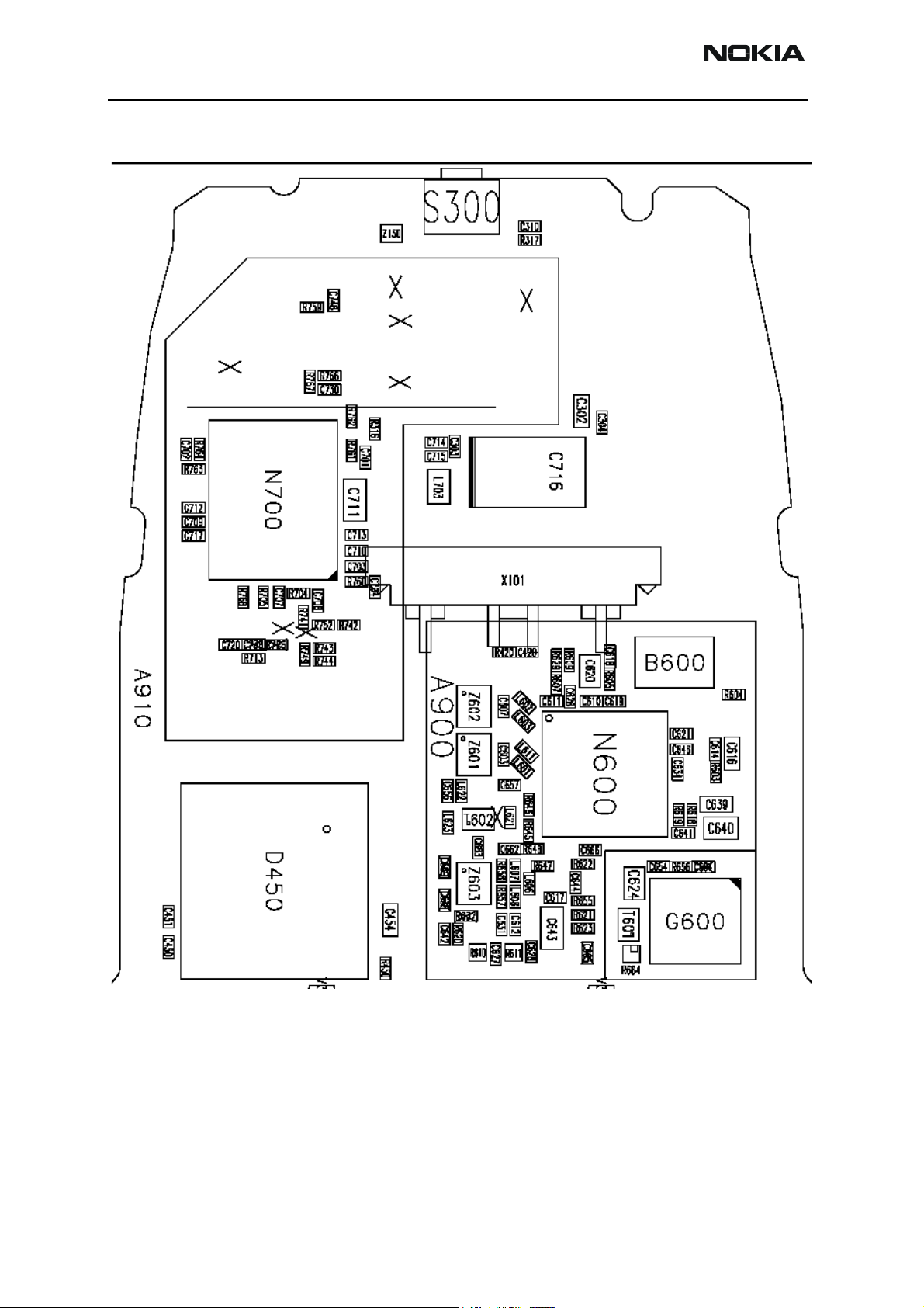
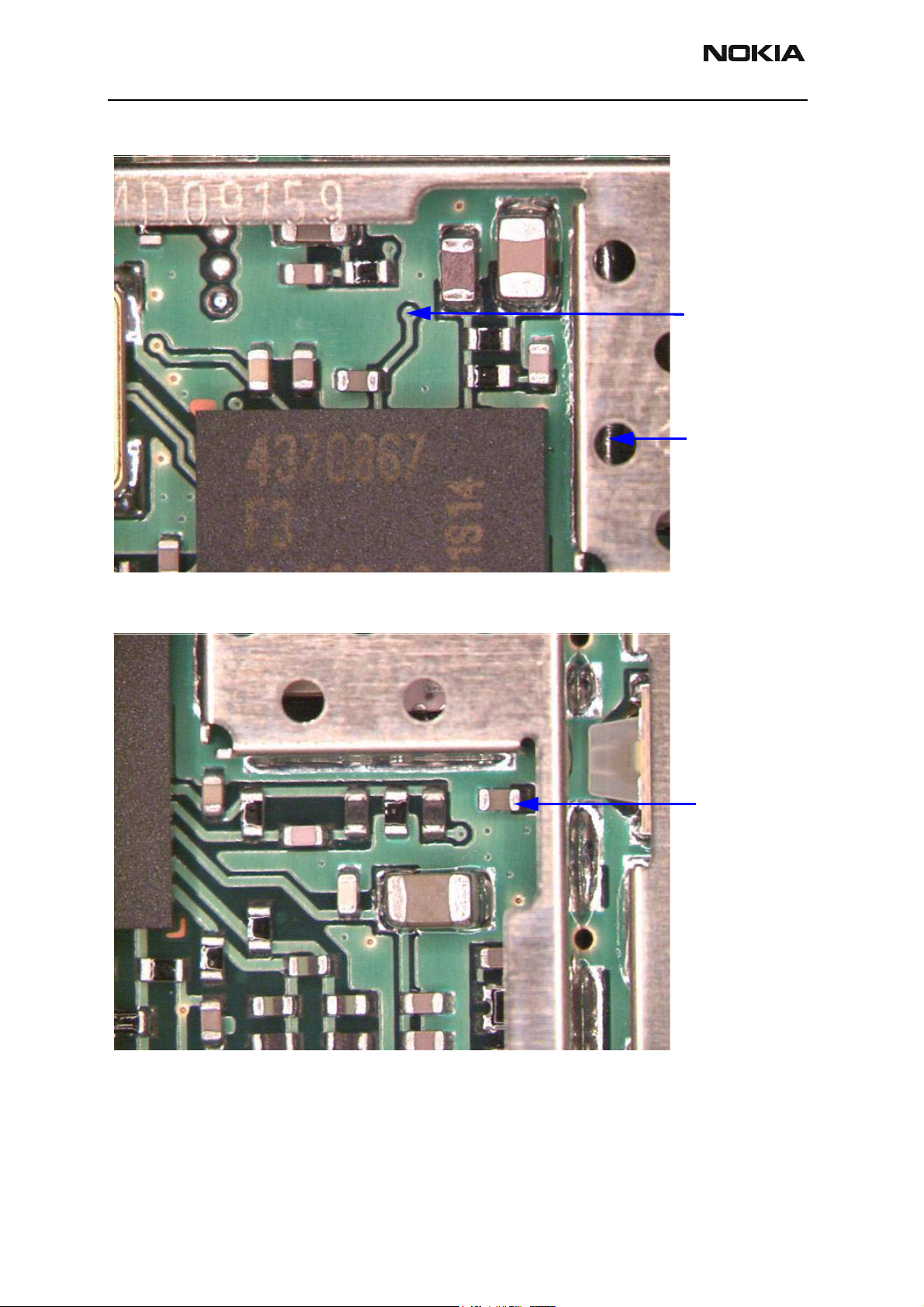
Refer to Table 3 and Figure 4 for key RF component locations.
Table 3: Key RF Components
Component Description
N600 Mjoelner RF IC
Z601 PCS Rx SAW
Z602 GSM Rx SAW
Z603 GSM Tx SAW
B600 26MHz crystal
G600 VCO (3.6GHz UHF VCO)
N700 Front End Module (FEM)
Issue 2 03/2004 ©2004 Nokia Corporation Confidential Page 7
Page 8
NPM-10 (3595)
Troubleshooting - RF CC Technical Documentation
Figure 4: Key RF Component Locations
Power Supply Configuration
All power supplies for the RF unit are generated in the UEM IC (D200). All power outputs
from this IC have a decoupling capacitor at which the supply voltage can be checked.
Page 8 ©2004 Nokia Corporation Confidential Issue 2 03/2004
Page 9
NPM-10 (3595)
CC Technical Documentation Troubleshooting - RF
Figure 5 shows the power supply configuration used in the NPM-10 (3595) phone.
PA
UEM
Battery
VR2
VR3
VR5
VR1A
VR6
VIO
MJOELNER
Vtx
VXO
VPLL
VCP
Vrx
Vbb
Vref1
VddXO
Vddbbb
VddRXF
VddRXBB
Vbext
VddTX
Vdddig
VddPLL
VddLO
VddPre
VddCP
Sel_addr
VddDL
Vref01
VR7
Vvco
VCO
module
Figure 5: Power supply configuration
The names in bold are signal names, which are used in the RF schematics. The names in
the boxes within the Mjoelner and VCO refer to pin names on the respective ICs (N600,
G600).
Table 4: Power Supply Details
RF Supply
Name
VTX VR2 2.64 2.78 2.86 V
VXO VR3 2.64 2.78 2.86 V
VCP VR1A 4.75 V
VPLL VR5 2.64 2.78 2.86 V
UEM Supply
Name
Minimum Type Maximum Unit
VRX VR6 2.64 2.78 2.86 V
VVCO VR7 2.64 2.78 2.86 V
VBB VIO 1.72 1.8 1.88 V
VREF2 VrelRF01 1.334 1.35 1.366 V
VBATT BATTERY 3.1 3.6 5.2 V
Issue 2 03/2004 ©2004 Nokia Corporation Confidential Page 9
Page 10
NPM-10 (3595)
Troubleshooting - RF CC Technical Documentation
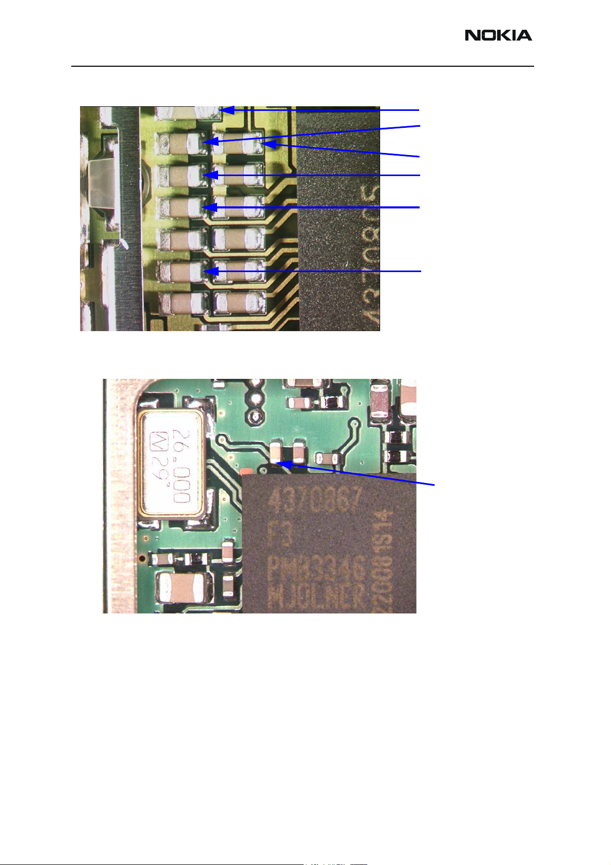
Figure 6 shows the measuring points at the UEM (D200).
VR2=Vtx (C643)
VR5=Vpll (C226)
VR7=Vvco (C224)
VR3=Vvcxo (C227)
VR6=Vrx (C225)
Vref01=Vref2 (C231)
Figure 6: Supply points at the UEM (D200)
Figure 7 shows the supply point at the Mjoelner (N600).
Figure 7: Supply point at the Mjoelner (N600)
Vio=Vbb (C621)
Receiver
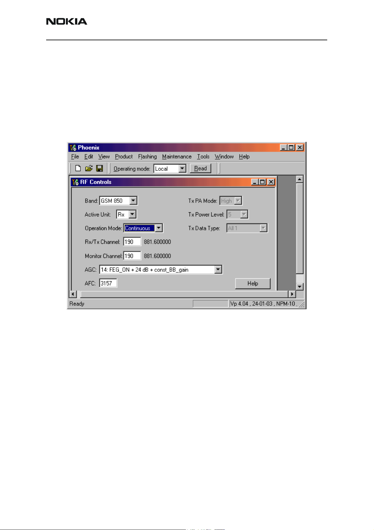
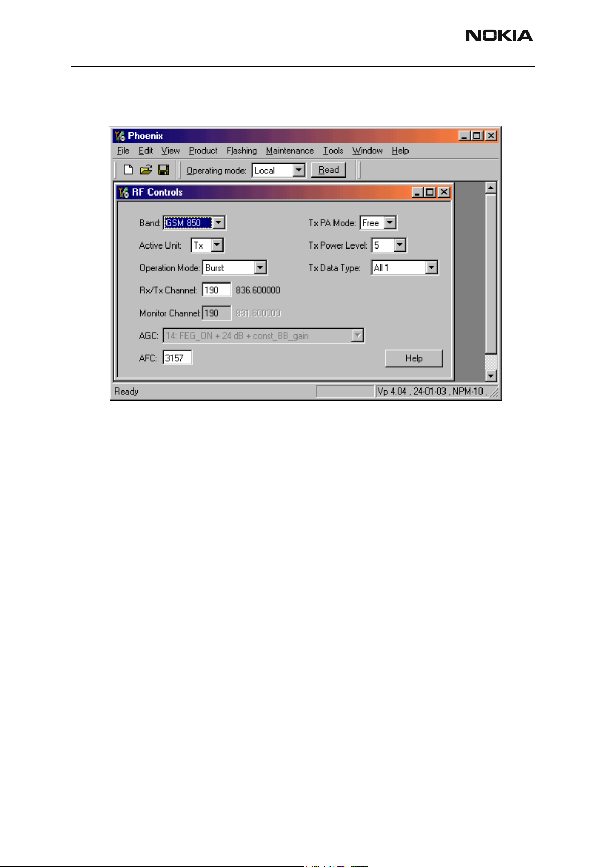
General Instructions for GSM 850 Rx Troubleshooting
Use the following steps to troubleshoot the GSM 850 Rx:
1. Connect the phone to a PC with the module test jig.
2. Start Phoenix, and establish a connection to the phone.
3. Open the File menu, and click Scan for Product.
Page 10 ©2004 Nokia Corporation Confidential Issue 2 03/2004
Page 11
NPM-10 (3595)
CC Technical Documentation Troubleshooting - RF
4. Open the Maintenance menu, point to Testing, and click RF Controls.
5. Select the following values on the RF Controls dialog box:
• Band = GSM 850
• Active Unit = Rx
• Operation Mode = Continuous
• Rx/Tx Channel = 190
• AGC = 9
Figure 8: GSM 850 Rx values on the RF Controls dialog box
Issue 2 03/2004 ©2004 Nokia Corporation Confidential Page 11
Page 12
NPM-10 (3595)
Troubleshooting - RF CC Technical Documentation
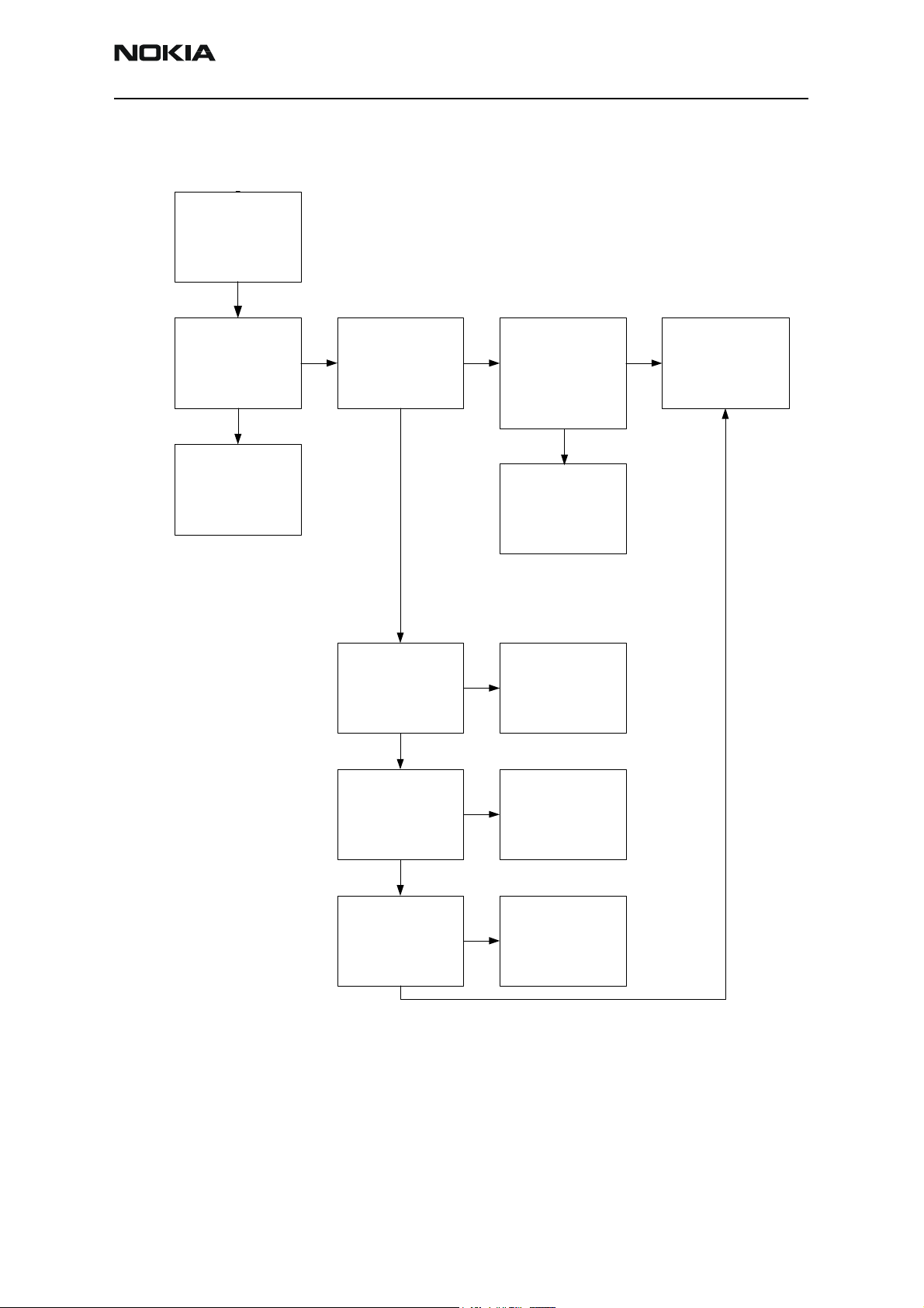
Troubleshooting Chart for the GSM 850 Receiver
1
Apply -55 dBm
881.6 MHz,
1
offset 67.71 kHz
from generator to
antenna connector
2
3
4
YES
Oscilloscope at
RX I/Q signal
2
704 mVpp
DC offset 1.38 V
freq. 67.64 kHz
NO
Check FEM
RX 850 at
Pin6 of N700
-56 dBm
NO
Oscilloscope
check
VANT1,VANT2
and VANT3 at
N70
0
signal 0V
NO
Check Mjoelner
YES
YES
3
GSM chain
functional
YES
Check
FEM
Spectrum analyzer
4
GSM SAW filter
Z602
output -59 dBm
NO
Check SAW filter
Z602
YES
YES
Spectrum analyzer
Check signal after
5
inductors L603 and
L602
-59 dBm
NO
Check inductors
L603, L602
YES
Oscilloscope
6
VRX 2.7 V
check Mjoelner
serial interface
NO
Check Base band
Figure 9: GSM 850 receiver troubleshooting chart
Page 12 ©2004 Nokia Corporation Confidential Issue 2 03/2004
Page 13
NPM-10 (3595)
CC Technical Documentation Troubleshooting - RF
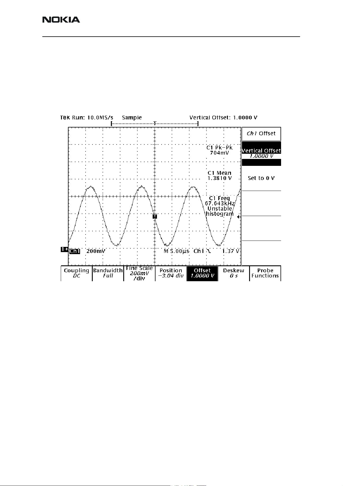
Figure 10 shows the results of measuring with an oscilloscope at RXIP or RXQP on a
working GSM 850 receiver.
• Signal general frequency = 881.66771 MHz
• Amplitude = -55 dBm
• Signal amplitude peak = 704 mV
• DC offset = 1.38 V
Figure 10: RX850 I/Q signal waveform
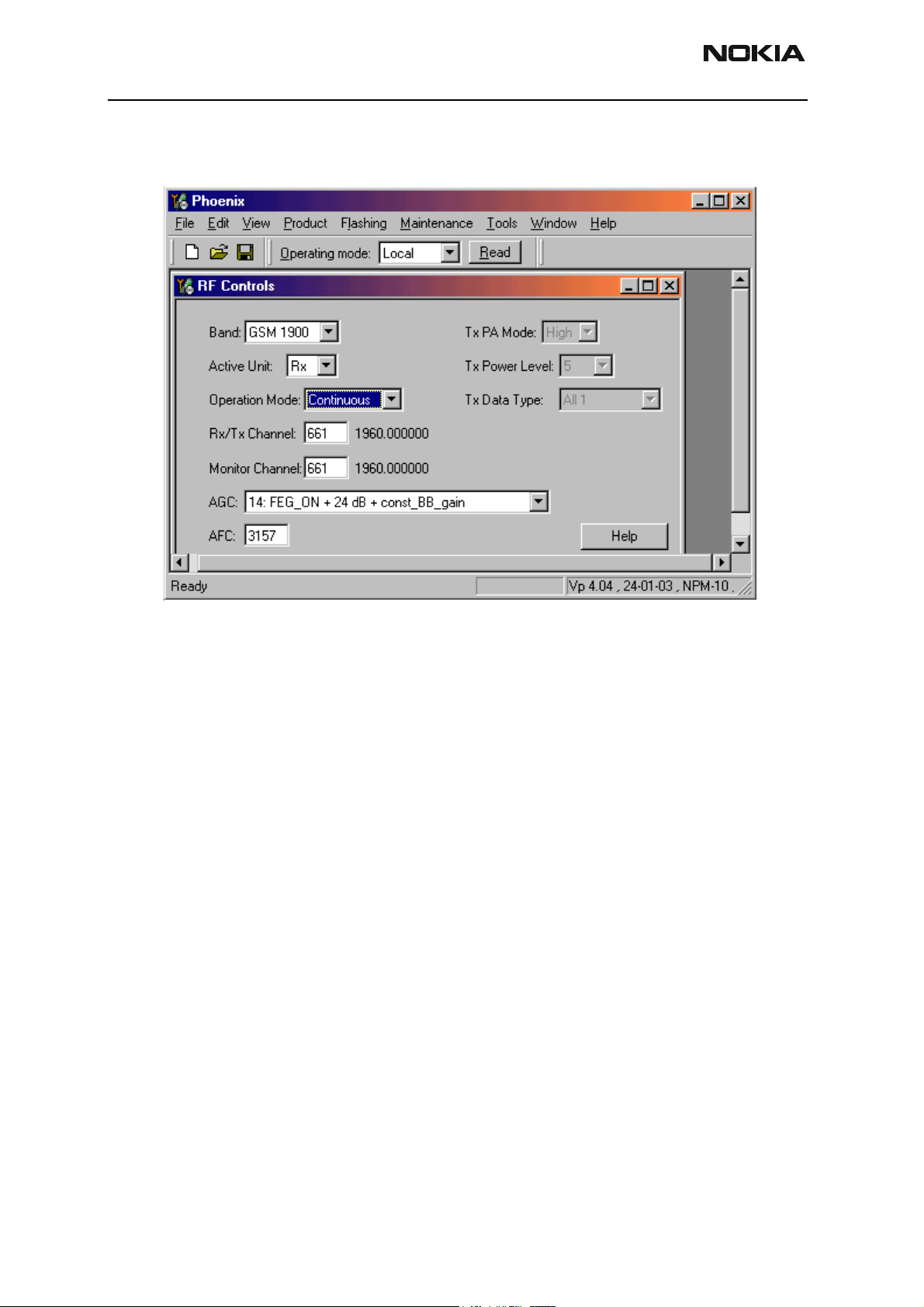
General Instructions for GSM 1900 Rx Troubleshooting
Use the following steps to troubleshoot the GSM 1900 Rx:
1. Connect the phone to a PC with the module test jig.
2. Start Phoenix, and establish a connection to the phone.
3. Open the File menu, and click Scan for Product.
4. Open the Maintenance menu, point to Testing, and click RF Controls.
5. Select the following values on the RF Controls dialog box:
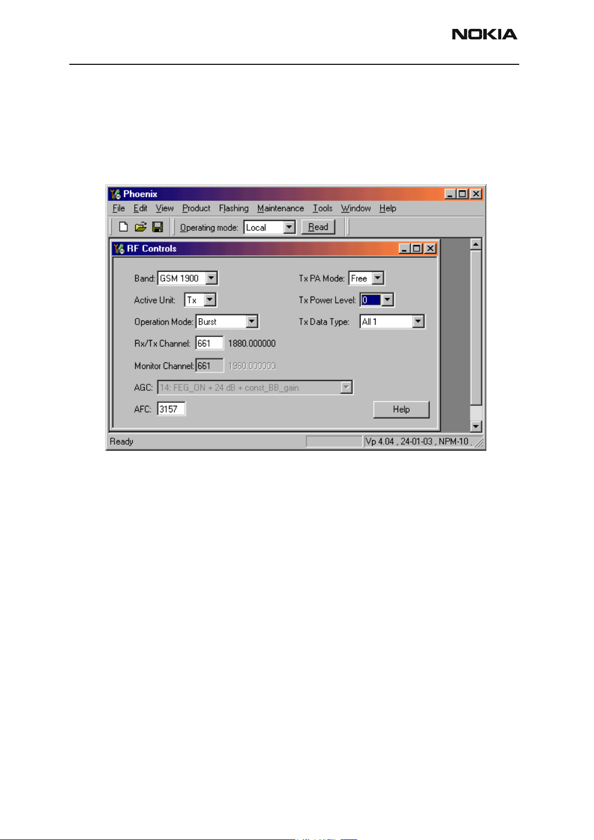
• Band = GSM 1900
• Active Unit = Rx
• Operation Mode = Continuous
Issue 2 03/2004 ©2004 Nokia Corporation Confidential Page 13
Page 14
NPM-10 (3595)
Troubleshooting - RF CC Technical Documentation
• Rx/Tx Channel = 661
• AGC = 9
Figure 11: GSM 1900 values on the Rx RF Controls dialog box
Page 14 ©2004 Nokia Corporation Confidential Issue 2 03/2004
Page 15
NPM-10 (3595)
CC Technical Documentation Troubleshooting - RF
Troubleshooting Chart for PCS Receiver
1
Apply -55 dBm
1960 MHz,
1
offset 67.71 kHz
from generator to
antenna connector
2
3
YES
4
Oscilloscope at
RX I/Q signal
2
416 mVpp
DC offset 1.35 V
freq. 67.68 kHz
NO
Check FEM
RX 1900
at Pin 8 of N700
-58 dBm
NO
YES
Oscilloscope
check
VANT1,VANT2
and
VANT2 at
N700
signal 0V
NO
Check
Mjoelner
YES
3
4
PCS chain
functional
YES
Spectrum analyzer
PCS SAW filter
Z601
output -66 dBm
NO
Check
FEM
Check SAW filter
Z601
YES
YES
Spectrum analyzer
Check signal after
5
inductors L611 and
L601
-66 dBm
NO
Check inductors
L611, L601
YES
Oscilloscope
6
VRX 2.7 V
check Mjoelner
serial interface
NO
Check Base band
Figure 12: GSM 1900 receiver troubleshooting chart
Issue 2 03/2004 ©2004 Nokia Corporation Confidential Page 15
Page 16

NPM-10 (3595)
Troubleshooting - RF CC Technical Documentation
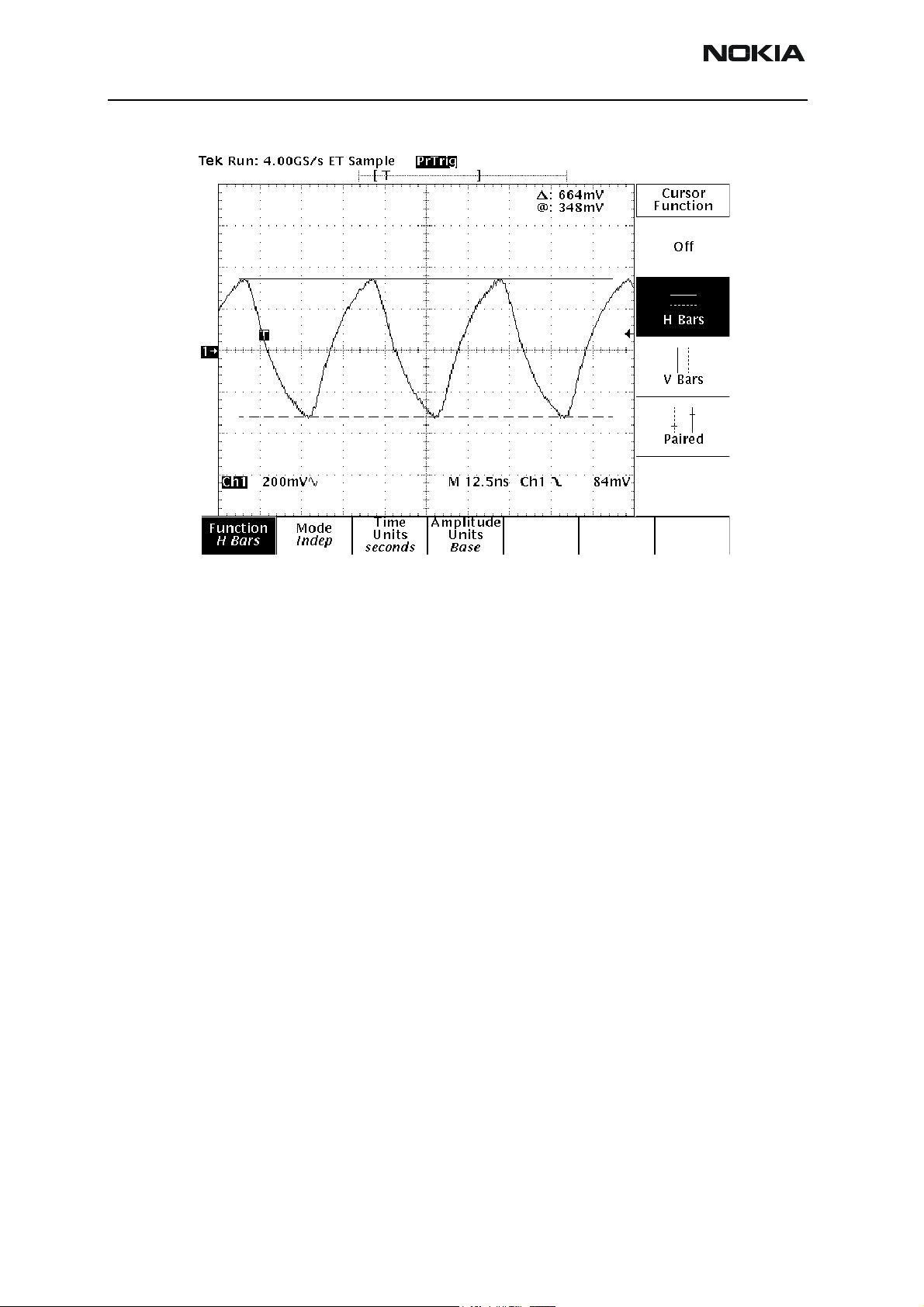
Figure 13 shows the results of measuring with an oscilloscope at RXIP or RXQP on a
working GSM 1900 receiver.
• Signal general frequency = 1960.06771 MHz
• Amplitude = -55 dBm
• Signal amplitude peak-peak 416 mV
• DC offset 1.35 V
Figure 13: RX1900 I/Q signal waveform
Page 16 ©2004 Nokia Corporation Confidential Issue 2 03/2004
Page 17
NPM-10 (3595)
CC Technical Documentation Troubleshooting - RF
Measurement Points in the Receiver
VANT1
Z700
VANT3
N700
Figure 14: Rx measurement points at the front-end module PA (N700)
RX850
Mjoelner input INML
L602
RX850
SAW filter
bal output
Z602
RF Antenna
(RX in)
N700
RX850
Mjoelner input INPL
L603
VANT2
Z700
RX1900
Mjoelner input INMM
L611
RX850
Mjoelner input INPM
L601
RX1900
SAW filter
bal output
Z601
RX850
SAW filter unbal input
Z602
Figure 15: Measurement points at the Rx filters – Z601/Z602
RX1900
SAW filter unbal input
Z601
Issue 2 03/2004 ©2004 Nokia Corporation Confidential Page 17
Page 18

NPM-10 (3595)
Troubleshooting - RF CC Technical Documentation
RXQM
D200
RXIM
D200
Figure 16: Rx I/Q Signals, baseband shielding can
Transmitter
Measurement Points for the Transmitter
RXIP
D200
RXQP
D200
VANT1
VANT3
ANT
(Tx out)
VANT2
Figure 17: Tx measurement points in the PA (N700) shielding can
VTXLO_G
VTX_B_P
OUT_D_TX
DET
VPCTRL_G
Page 18 ©2004 Nokia Corporation Confidential Issue 2 03/2004
Page 19

NPM-10 (3595)
CC Technical Documentation Troubleshooting - RF
VTX
TXQM
TXQP
TXIP
Bal_Input2
PCS
OUT_D_TX
Figure 18: Tx measurement points in the Mjolner (N600) shielding can
Bal_Input1
PCS
Bal_Input1
GSM
OUT_G_TX
General Instructions for GSM Tx Troubleshooting
Use the following steps to troubleshoot the GSM Tx:
1. Apply an RF cable to the RF connector to allow the transmitted signal to act as
normal. The RF cable should be connected to measurement equipment with at
least a 10 dB attenuator. Otherwise, the test equipment may be damaged.
2. Start Phoenix, and establish a connection to the phone (e.g., FBUS, MBUS).
3. Open the File menu, and click Choose Product.
4. Select NPM-10.
TXIM
Bal_Input2
GSM
5. Open the Maintenance menu, point to Testing, and click RF Controls.
6. Select the following values on the RF Controls dialog box:
• Band = GSM 850
• Active Unit = Tx
• Operation Mode = Burst
• Rx/Tx Channel = 190
• Tx PA Mode = Free
Issue 2 03/2004 ©2004 Nokia Corporation Confidential Page 19
Page 20
NPM-10 (3595)
Troubleshooting - RF CC Technical Documentation
• Tx Power Level = 5
• Tx Data Type = All 1
Figure 19: GSM Tx values on the RF Controls dialog box
7 Measure the output power of the phone; it should be around 32.0 dBm.
Remember the loss along the end launch connector in the test jig
(around 0.3 dB).
Page 20 ©2004 Nokia Corporation Confidential Issue 2 03/2004
Page 21
NPM-10 (3595)
CC Technical Documentation Troubleshooting - RF
Troubleshooting Chart for GSM 850 Transmitter
Use a high impedance probe for the spectrum analyzer measurements in the following
chart. Set the trace to maxhold because the signal is bursted.
Measure power on
ANT with power
meter or RCT
>31dBm
Yes
Check R759, C746
Measure pin 1 of
No No No No
FEM: -0dBm
Yes
Check FEM with
scope:
Vant1= 2.4 to 2.8V
Vant2, Vant3= 0V
VTX_B_P= 0
VTXLO_G= 2.8V
Yes
No
Measure BAL
input to Z603
0dBm
Check Z603
(TX SAW filter)
Check VTX with
scope: 2.8V +
discretes around
YesYes
Check TX IP and
TXQP
(See Figure 22)
Yes
Check baseband
No
Check VPCTRL_G
with scope at pin
15 of N700
(See Figure 21)
Yes
Check N700
(FEM)
No
Check TXC with
scope
(See Figure 21)
Yes
Check Det with
scope
(See Figure 21)
Yes
Check N700
(detector) +
discrete around
Figure 20: GSM 850 transmitter troubleshooting chart
The following apply to Figure 21:
• GSM 850 band, Power level 5, Channel 190
•Black trace: TXP
• Green trace: TXC
• Red trace: Vpctrl_G @ R713 output
No
No
Check Mjoelner +
the serial bus
• Blue trace: VDet_G @ R704 input
Issue 2 03/2004 ©2004 Nokia Corporation Confidential Page 21
Page 22

NPM-10 (3595)
Troubleshooting - RF CC Technical Documentation
Figure 21: TXP, VPCTRL_G and TXC
Page 22 ©2004 Nokia Corporation Confidential Issue 2 03/2004
Page 23

NPM-10 (3595)
CC Technical Documentation Troubleshooting - RF
Troubleshooting the Modulation
The following plots show different situations of Tx IQ measurements. Depending on the
time, the modulation may cause the signal to look differently.
Pink trace: TXQP Blue trace: TXIP - All 1 Pink trace: TXQP Bluetrace: TXIP - Random
Pink trace: TXQP Blue trace: TXIP - All 1 (Zoom In)
Figure 22: Tx I/Q waveforms
Pink trace: TXQP Blu etrace: TXIP - Random ( Zoom In)
I/Q signals look almost the same regardless if modulation is by "1" or by "0". There is no
significant difference between TXIP and TXIM. The same is valid for TXQP and TXQM.
General instructions for PCS Tx troubleshooting
Use the following steps to troubleshoot the PCS Tx:
1. Apply an RF cable to the RF connector to allow the transmitted signal to act as
normal. The RF cable should be connected to measurement equipment or at least
to a 10 dB attenuator. Otherwise, the test equipment may be damaged.
2. Start Phoenix, and establish a connection to the phone (e.g., FBUS).
3. Open the File menu, and click Choose Product.
4. Select NPM-10.
5. Open the Maintenance menu, point to Testing, and click RF Controls.
Issue 2 03/2004 ©2004 Nokia Corporation Confidential Page 23
Page 24
NPM-10 (3595)
Troubleshooting - RF CC Technical Documentation
6. Select the following values on the RF Controls dialog box:
• Band = GSM 1900
• Active Unit = Tx
• Tx Power Level = 0
• Tx Data Type = All 1
Figure 23: PCS Tx values on the RF Controls dialog box
7. Measure the output power of the phone; it should be around 29.5 dBm.
Remember the loss in the test jig (around 0.7 dB).
Page 24 ©2004 Nokia Corporation Confidential Issue 2 03/2004
Page 25

NPM-10 (3595)
CC Technical Documentation Troubleshooting - RF
Figure 24 shows a troubleshooting chart for the PCS transmitter
Measure power on
ANT with power
meter or RCT
>28dBm
Yes
Check R759, C746
No No No No
Measure
Pin_PCS:
-2dBm
Yes
Check FEM with
scope:
Vant1,Vant3 = 0
Vant2, Vant4=
2.4 to 2.8 V
VTX_B_P and
VTXLO_G= 2.8V
Yes
No
Measure BAL
input to T600
-4dBm
Check T602
(PCS Balun)
Check VTX with
scope: 2.7V +
discretes around
YesYes
Check TXIP and
TXQP
(See Figure 22)
Yes
Check baseband
No
Check VPCTRL_P
with scope
(See Figure 25)
Yes
Check N700
(FEM)
No
Check TXC with
scope
(See Figure 25)
Yes
Check Det with
scope
(See Figure 25)
Yes
Check N700
(detector) +
discrete around
No
No
Figure 24: GSM 1900 transmitter troubleshooting chart
Check Mjoelner +
the serial bus
Issue 2 03/2004 ©2004 Nokia Corporation Confidential Page 25
Page 26

NPM-10 (3595)
Troubleshooting - RF CC Technical Documentation
The following applies to Figure 25:
• PCS 1900 band, Power level 0, Channel 661
• Red trace: Vpctrl_P @ R713 output
Figure 25: VPCTRL_P
Note: TXIQ signals look the same in PCS and GSM
Synthesizer
There is only one PLL synthesizer generating local oscillator frequencies for both the Rx
and Tx in both bands (PCS and GSM). The VCO frequency is divided by two for PCS
operation or by four for GSM operation inside the Mjoelner IC.
General Instructions for Synthesizer Troubleshooting
Use the following steps to troubleshoot the synthesizer:
1. Start Phoenix, and establish a connection to the phone.
2. Open the File menu, and click Choose Product.
3. Select NPM-10.
4. Open the Maintenance menu, point to Testing, and click RF Controls.
5. Select the following values on the RF Controls dialog box:
• Band = GSM 1900
• Active Unit = Rx
Page 26 ©2004 Nokia Corporation Confidential Issue 2 03/2004
Page 27

NPM-10 (3595)
CC Technical Documentation Troubleshooting - RF
• Operation Mode = Continuous
• Rx/Tx Channel = 661
Figure 26: Synthesizer values on the RF Controls dialog box
It is not possible to measure the output of the VCO (G600) directly because this component is placed underneath a shielding can without a detachable lid. However, it is
possible to get an indication if the VCO outputs the correct frequency with a spectrum
analyzer and a high impedance probe. To do this, probe R656 and C654. The frequency
should be 3920 MHz and the power should be around –50 dBm.
26 MHz Reference Oscillator (VCXO)
The 26 MHz oscillator is located in the Mjoelner IC (N600). The coarse frequency for this
oscillator is set by an external crystal (B600). The oscillator is used as a reference
frequency for the PLL synthesizer and as the system clock for the baseband. The 26 MHz
signal is divided by two to achieve 13 MHz inside the UPP IC (D400). The 26 MHz signal
from the VCXO can be measured by probing R420 (measure on the UPP side of R420,
which is the end that is not connected to C420). The level at this point is approximately
700 mVpp. The frequency of this oscillator is adjusted by changing the AFC-register
inside the Mjoelner IC via the Mjoelner serial interface.
Issue 2 03/2004 ©2004 Nokia Corporation Confidential Page 27
Page 28
NPM-10 (3595)
Troubleshooting - RF CC Technical Documentation
Example Signal Measured at VCXO output (R420)
Figure 27: VCXO 26 MHz waveform
VCO
The VCO generates frequencies in the range of 3296.8 MHz–3979.6 MHz when the PLL is
running. The output frequency from the VCO is led to the local oscillator input of the
Mjoelner IC (N600), where the frequency is divided by two or four so that they can
generate all channels in GSM and PCS respectively. The frequency of the VCO is
controlled by a DC-voltage (Vctrl) coming from the loop filter. The loop filter consists of
the R618, R619, and C639-C641 components. The Vctrl range when the PLL is running
(locked) is 0.4 V–2.4 V. Even if the PLL is not in a locked state (the Vctrl is out of range),
there is some frequency at the output of the VCO (G600), which is between 3 GHz and 4
GHz. This is only true if the VCO is working and if the VCO power supply is present
(2.7 V).
Troubleshooting Chart for PLL Synthesizer
Use the following settings in Pheonix to troubleshoot the PLL synthesizer in Figure 29.
1. Open the File menu, and click Choose Product.
2. Select NPM-10.
3. Open the Maintenance menu, point to Testing, and click RF Controls.
4. Select the following values on the RF Controls dialog box:
• Band = GSM 1900
• Active Unit = Rx
Page 28 ©2004 Nokia Corporation Confidential Issue 2 03/2004
Page 29

NPM-10 (3595)
CC Technical Documentation Troubleshooting - RF
• Operation Mode = Continuous
• Rx/Tx Channel = 661
Figure 28: RF Controls settings for PLL troubleshooting
5. Troubleshoot using Figure 29.
Issue 2 03/2004 ©2004 Nokia Corporation Confidential Page 29
Page 30
NPM-10 (3595)
Troubleshooting - RF CC Technical Documentation
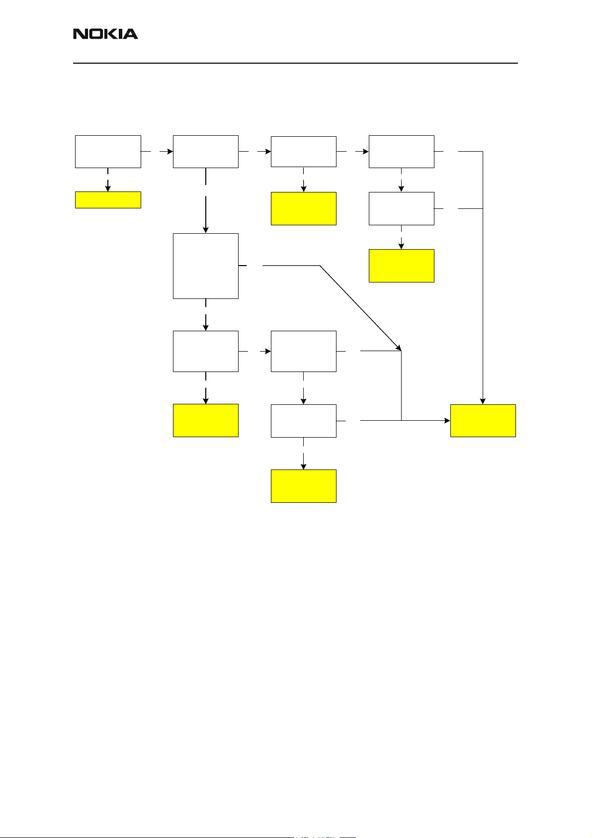
Spectrum analyzer VCO
frequency (R656) 3920.0
MHz
No
Yes
PLL block functional
Oscilloscope VCXO power
supply (C620) 2.7 V
Yes
Oscilloscope VC XO out put
(R420) 26 MHz,
approx. 700 mVpp
Yes
Oscilloscope VCO power
supply (R656) 2.7 V
Yes
Oscilloscope PLL powe r
supply (C665 and C634)
ALL 2.7 V
No
No
No
No
Check UEM, Software,
phone not in function
VCXO is not functiona l,
check crystal (B6 00)
Check UEM, software,
phone not in function
Check UEM, software,
phone not in function
Yes
Spectrum analyzer VCO
output (R656) some signal
between 4 GHz and 4 GHz
Yes
Oscilloscope: Measure
control voltage (C641 )
between 0.5 V and 4.0 V
Yes
Check Mjoe lner (N600), UPP
(D400), FRBusClk (J608),
RFBusDA (J610), FRBusX
(J609), and Reset_Mjoel
Figure 29: PLL troubleshooting chart
No
No
VCO (N601) is not
functional
Check loop filter R618,
R619, C639-C641
Page 30 ©2004 Nokia Corporation Confidential Issue 2 03/2004
Page 31

NPM-10 (3595)
CC Technical Documentation Troubleshooting - RF
If the phone stops working a short time after the power is turned ON, the 26 MHz system
clock signal might not be getting to the UPP clock-input in the baseband. In this case,
turn on the phone and verify the following:
• VCXO power supply (C620) = 2.7 V
• VCXO output (R420 – the end not connected to C420) is 26 MHz and approximately 700 mVpp
If this is not the case, check the reference crystal (B600), Mjoelner (N600), R420, R426,
C420, and C426.
Measurement Points for the PLL
VCXO Vcc (C620)
VCXO Output
(R420)
Measure at this
end!
Figure 30: Measurement point for VCXO supply
Figure 31: Measurement point for VCXO output
Issue 2 03/2004 ©2004 Nokia Corporation Confidential Page 31
Page 32
NPM-10 (3595)
h
t
Troubleshooting - RF CC Technical Documentation
Measurement Points at the PLL/VCO
PLL Vcc (C634)
VCO Vcc (C654,
R656)
Be careful - do not
short this point wit
shield. The VCO Ou
put is also detected
here.
Figure 32: Measurement points at the PLL/VCO
PLL Vcc (C665)
Figure 33: Measurement point for PLL
Page 32 ©2004 Nokia Corporation Confidential Issue 2 03/2004
Page 33

NPM-10 (3595)
CC Technical Documentation Troubleshooting - RF
Frequency Lists
GSM 850
Ch TX RX VCO TX VCO RX Ch TX RX VCO TX VCO RX Ch TX RX VCO TX VCO RX
128 824.2 869.2 3296.8 3476.8 170 832.6 877.6 3330.4 3510.4 210 840.6 885.6 3362.4 3542.4
129 824.4 869.4 3297.6 3477.6 171 832.8 877.8 3331.2 3511.2 211 840.8 885.8 3363.2 3543.2
130 824.6 869.6 3298.4 3478.4 172 833 878 3332 3512 212 841 886 3364 3544
131 824.8 869.8 3299.2 3479.2 173 833.2 878.2 3332.8 3512.8 213 841.2 886.2 3364.8 3544.8
132 825 870 3300 3480 174 833.4 878.4 3333.6 3513.6 214 841.4 886.4 3365.6 3545.6
133 825.2 870.2 3300.8 3480.8 175 833.6 878.6 3334.4 3514.4 215 841.6 886.6 3366.4 3546.4
134 825.4 870.4 3301.6 3481.6 176 833.8 878.8 3335.2 3515.2 216 841.8 886.8 3367.2 3547.2
135 825.6 870.6 3302.4 3482.4 177 834 879 3336 3516 217 842 887 3368 3548
136 825.8 870.8 3303.2 3483.2 178 834.2 879.2 3336.8 3516.8 218 842.2 887.2 3368.8 3548.8
137 826 871 3304 3484 179 834.4 879.4 3337.6 3517.6 219 842.4 887.4 3369.6 3549.6
138 826.2 871.2 3304.8 3484.8 180 834.6 879.6 3338.4 3518.4 220 842.6 887.6 3370.4 3550.4
139 826.4 871.4 3305.6 3485.6 181 834.8 879.8 3339.2 3519.2 221 842.8 887.8 3371.2 3551.2
140 826.6 871.6 3306.4 3486.4 182 835 880 3340 3520 222 843 888 3372 3552
141 826.8 871.8 3307.2 3487.2 183 835.2 880.2 3340.8 3520.8 223 843.2 888.2 3372.8 3552.8
142 827 872 3308 3488 184 835.4 880.4 3341.6 3521.6 224 843.4 888.4 3373.6 3553.6
143 827.2 872.2 3308.8 3488.8 185 835.6 880.6 3342.4 3522.4 225 843.6 888.6 3374.4 3554.4
144 827.4 872.4 3309.6 3489.6 186 835.8 880.8 3343.2 3523.2 226 843.8 888.8 3375.2 3555.2
145 827.6 872.6 3310.4 3490.4 187 836 881 3344 3524 227 844 889 3376 3556
146 827.8 872.8 3311.2 3491.2 188 836.2 881.2 3344.8 3524.8 228 844.2 889.2 3376.8 3556.8
147 828 873 3312 3492 189 836.4 881.4 3345.6 3525.6 229 844.4 889.4 3377.6 3557.6
148 828.2 873.2 3312.8 3492.8 190 836.6 881.6 3346.4 3526.4 230 844.6 889.6 3378.4 3558.4
149 828.4 873.4 3313.6 3493.6 191 836.8 881.8 3347.2 3527.2 231 844.8 889.8 3379.2 3559.2
150 828.6 873.6 3314.4 3494.4 192 837 882 3348 3528 232 845 890 3380 3560
151 828.8 873.8 3315.2 3495.2 193 837.2 882.2 3348.8 3528.8 233 845.2 890.2 3380.8 3560.8
152 829 874 3316 3496 194 837.4 882.4 3349.6 3529.6 234 845.4 890.4 3381.6 3561.6
153 829.2 874.2 3316.8 3496.8 195 837.6 882.6 3350.4 3530.4 235 845.6 890.6 3382.4 3562.4
154 829.4 874.4 3317.6 3497.6 196 837.8 882.8 3351.2 3531.2 236 845.8 890.8 3383.2 3563.2
155 829.6 874.6 3318.4 3498.4 197 838 883 3352 3532 237 846 891 3384 3564
156 829.8 874.8 3319.2 3499.2 198 838.2 883.2 3352.8 3532.8 238 846.2 891.2 3384.8 3564.8
157 830 875 3320 3500 199 838.4 883.4 3353.6 3533.6 239 846.4 891.4 3385.6 3565.6
158 830.2 875.2 3320.8 3500.8 200 838.6 883.6 3354.4 3534.4 240 846.6 891.6 3386.4 3566.4
159 830.4 875.4 3321.6 3501.6 201 838.8 883.8 3355.2 3535.2 241 846.8 891.8 3387.2 3567.2
160 830.6 875.6 3322.4 3502.4 202 839 884 3356 3536 242 847 892 3388 3568
161 830.8 875.8 3323.2 3503.2 203 839.2 884.2 3356.8 3536.8 243 847.2 892.2 3388.8 3568.8
162 831 876 3324 3504 204 839.4 884.4 3357.6 3537.6 244 847.4 892.4 3389.6 3569.6
163 831.2 876.2 3324.8 3504.8 205 839.6 884.6 3358.4 3538.4 245 847.6 892.6 3390.4 3570.4
164 831.4 876.4 3325.6 3505.6 206 839.8 884.8 3359.2 3539.2 246 847.8 892.8 3391.2 3571.2
165 831.6 876.6 3326.4 3506.4 207 840 885 3360 3540 247 848 893 3392 3572
166 831.8 876.8 3327.2 3507.2 208 840.2 885.2 3360.8 3540.8 248 848.2 893.2 3392.8 3572.8
167 832 877 3328 3508 209 840.4 885.4 3361.6 3541.6 249 848.4 893.4 3393.6 3573.6
168 832.2 877.2 3328.8 3508.8 250 848.6 893.6 3394.4 3574.4
169 832.4 877.4 3329.6 3509.6 251 848.8 893.8 3395.2 3575.2
Issue 2 03/2004 ©2004 Nokia Corporation Confidential Page 33
Page 34
NPM-10 (3595)
Troubleshooting - RF CC Technical Documentation
PCS 1900
Ch TX RX VCO TX VCO RX Ch T X RX VCO TX VCO RX Ch T X RX VCO TX VCO RX
512 1850.2 1930.2 3700.4 3860.4 612 1870.2 1950.2 3740.4 3900.4 712 1890.2 1970.2 3780.4 3940.4
513 1850.4 1930.4 3700.8 3860.8 613 1870.4 1950.4 3740.8 3900.8 713 1890.4 1970.4 3780.8 3940.8
514 1850.6 1930.6 3701.2 3861.2 614 1870.6 1950.6 3741.2 3901.2 714 1890.6 1970.6 3781.2 3941.2
515 1850.8 1930.8 3701.6 3861.6 615 1870.8 1950.8 3741.6 3901.6 715 1890.8 1970.8 3781.6 3941.6
516 1851 1931 3702 3862 616 1871 1951 3742 3902 716 1891 1971 3782 3942
517 1851.2 1931.2 3702.4 3862.4 617 1871.2 1951.2 3742.4 3902.4 717 1891.2 1971.2 3782.4 3942.4
518 1851.4 1931.4 3702.8 3862.8 618 1871.4 1951.4 3742.8 3902.8 718 1891.4 1971.4 3782.8 3942.8
519 1851.6 1931.6 3703.2 3863.2 619 1871.6 1951.6 3743.2 3903.2 719 1891.6 1971.6 3783.2 3943.2
520 1851.8 1931.8 3703.6 3863.6 620 1871.8 1951.8 3743.6 3903.6 720 1891.8 1971.8 3783.6 3943.6
521 1852 1932 3704 3864 621 1872 1952 3744 3904 721 1892 1972 3784 3944
522 1852.2 1932.2 3704.4 3864.4 622 1872.2 1952.2 3744.4 3904.4 722 1892.2 1972.2 3784.4 3944.4
523 1852.4 1932.4 3704.8 3864.8 623 1872.4 1952.4 3744.8 3904.8 723 1892.4 1972.4 3784.8 3944.8
524 1852.6 1932.6 3705.2 3865.2 624 1872.6 1952.6 3745.2 3905.2 724 1892.6 1972.6 3785.2 3945.2
525 1852.8 1932.8 3705.6 3865.6 625 1872.8 1952.8 3745.6 3905.6 725 1892.8 1972.8 3785.6 3945.6
526 1853 1933 3706 3866 626 1873 1953 3746 3906 726 1893 1973 3786 3946
527 1853.2 1933.2 3706.4 3866.4 627 1873.2 1953.2 3746.4 3906.4 727 1893.2 1973.2 3786.4 3946.4
528 1853.4 1933.4 3706.8 3866.8 628 1873.4 1953.4 3746.8 3906.8 728 1893.4 1973.4 3786.8 3946.8
529 1853.6 1933.6 3707.2 3867.2 629 1873.6 1953.6 3747.2 3907.2 729 1893.6 1973.6 3787.2 3947.2
530 1853.8 1933.8 3707.6 3867.6 630 1873.8 1953.8 3747.6 3907.6 730 1893.8 1973.8 3787.6 3947.6
531 1854 1934 3708 3868 631 1874 1954 3748 3908 731 1894 1974 3788 3948
532 1854.2 1934.2 3708.4 3868.4 632 1874.2 1954.2 3748.4 3908.4 732 1894.2 1974.2 3788.4 3948.4
533 1854.4 1934.4 3708.8 3868.8 633 1874.4 1954.4 3748.8 3908.8 733 1894.4 1974.4 3788.8 3948.8
534 1854.6 1934.6 3709.2 3869.2 634 1874.6 1954.6 3749.2 3909.2 734 1894.6 1974.6 3789.2 3949.2
535 1854.8 1934.8 3709.6 3869.6 635 1874.8 1954.8 3749.6 3909.6 735 1894.8 1974.8 3789.6 3949.6
536 1855 1935 3710 3870 636 1875 1955 3750 3910 736 1895 1975 3790 3950
537 1855.2 1935.2 3710.4 3870.4 637 1875.2 1955.2 3750.4 3910.4 737 1895.2 1975.2 3790.4 3950.4
538 1855.4 1935.4 3710.8 3870.8 638 1875.4 1955.4 3750.8 3910.8 738 1895.4 1975.4 3790.8 3950.8
539 1855.6 1935.6 3711.2 3871.2 639 1875.6 1955.6 3751.2 3911.2 739 1895.6 1975.6 3791.2 3951.2
540 1855.8 1935.8 3711.6 3871.6 640 1875.8 1955.8 3751.6 3911.6 740 1895.8 1975.8 3791.6 3951.6
541 1856 1936 3712 3872 641 1876 1956 3752 3912 741 1896 1976 3792 3952
542 1856.2 1936.2 3712.4 3872.4 642 1876.2 1956.2 3752.4 3912.4 742 1896.2 1976.2 3792.4 3952.4
543 1856.4 1936.4 3712.8 3872.8 643 1876.4 1956.4 3752.8 3912.8 743 1896.4 1976.4 3792.8 3952.8
544 1856.6 1936.6 3713.2 3873.2 644 1876.6 1956.6 3753.2 3913.2 744 1896.6 1976.6 3793.2 3953.2
545 1856.8 1936.8 3713.6 3873.6 645 1876.8 1956.8 3753.6 3913.6 745 1896.8 1976.8 3793.6 3953.6
546 1857 1937 3714 3874 646 1877 1957 3754 3914 746 1897 1977 3794 3954
547 1857.2 1937.2 3714.4 3874.4 647 1877.2 1957.2 3754.4 3914.4 747 1897.2 1977.2 3794.4 3954.4
548 1857.4 1937.4 3714.8 3874.8 648 1877.4 1957.4 3754.8 3914.8 748 1897.4 1977.4 3794.8 3954.8
549 1857.6 1937.6 3715.2 3875.2 649 1877.6 1957.6 3755.2 3915.2 749 1897.6 1977.6 3795.2 3955.2
550 1857.8 1937.8 3715.6 3875.6 650 1877.8 1957.8 3755.6 3915.6 750 1897.8 1977.8 3795.6 3955.6
551 1858 1938 3716 3876 651 1878 1958 3756 3916 751 1898 1978 3796 3956
552 1858.2 1938.2 3716.4 3876.4 652 1878.2 1958.2 3756.4 3916.4 752 1898.2 1978.2 3796.4 3956.4
553 1858.4 1938.4 3716.8 3876.8 653 1878.4 1958.4 3756.8 3916.8 753 1898.4 1978.4 3796.8 3956.8
554 1858.6 1938.6 3717.2 3877.2 654 1878.6 1958.6 3757.2 3917.2 754 1898.6 1978.6 3797.2 3957.2
555 1858.8 1938.8 3717.6 3877.6 655 1878.8 1958.8 3757.6 3917.6 755 1898.8 1978.8 3797.6 3957.6
556 1859 1939 3718 3878 656 1879 1959 3758 3918 756 1899 1979 3798 3958
557 1859.2 1939.2 3718.4 3878.4 657 1879.2 1959.2 3758.4 3918.4 757 1899.2 1979.2 3798.4 3958.4
558 1859.4 1939.4 3718.8 3878.8 658 1879.4 1959.4 3758.8 3918.8 758 1899.4 1979.4 3798.8 3958.8
559 1859.6 1939.6 3719.2 3879.2 659 1879.6 1959.6 3759.2 3919.2 759 1899.6 1979.6 3799.2 3959.2
560 1859.8 1939.8 3719.6 3879.6 660 1879.8 1959.8 3759.6 3919.6 760 1899.8 1979.8 3799.6 3959.6
561 1860 1940 3720 3880 661 1880 1960 3760 3920 761 1900 1980 3800 3960
Page 34 ©2004 Nokia Corporation Confidential Issue 2 03/2004
Page 35
NPM-10 (3595)
CC Technical Documentation Troubleshooting - RF
Ch TX RX V CO T X V CO RX Ch TX RX VCO TX V CO RX Ch TX RX VCO TX V CO RX
562 1860.2 1940.2 3720.4 3880.4 662 1880.2 1960.2 3760.4 3920.4 762 1900.2 1980.2 3800.4 3960.4
563 1860.4 1940.4 3720.8 3880.8 663 1880.4 1960.4 3760.8 3920.8 763 1900.4 1980.4 3800.8 3960.8
564 1860.6 1940.6 3721.2 3881.2 664 1880.6 1960.6 3761.2 3921.2 764 1900.6 1980.6 3801.2 3961.2
565 1860.8 1940.8 3721.6 3881.6 665 1880.8 1960.8 3761.6 3921.6 765 1900.8 1980.8 3801.6 3961.6
566 1861 1941 3722 3882 666 1881 1961 3762 3922 766 1901 1981 3802 3962
567 1861.2 1941.2 3722.4 3882.4 667 1881.2 1961.2 3762.4 3922.4 767 1901.2 1981.2 3802.4 3962.4
568 1861.4 1941.4 3722.8 3882.8 668 1881.4 1961.4 3762.8 3922.8 768 1901.4 1981.4 3802.8 3962.8
569 1861.6 1941.6 3723.2 3883.2 669 1881.6 1961.6 3763.2 3923.2 769 1901.6 1981.6 3803.2 3963.2
570 1861.8 1941.8 3723.6 3883.6 670 1881.8 1961.8 3763.6 3923.6 770 1901.8 1981.8 3803.6 3963.6
571 1862 1942 3724 3884 671 1882 1962 3764 3924 771 1902 1982 3804 3964
572 1862.2 1942.2 3724.4 3884.4 672 1882.2 1962.2 3764.4 3924.4 772 1902.2 1982.2 3804.4 3964.4
573 1862.4 1942.4 3724.8 3884.8 673 1882.4 1962.4 3764.8 3924.8 773 1902.4 1982.4 3804.8 3964.8
574 1862.6 1942.6 3725.2 3885.2 674 1882.6 1962.6 3765.2 3925.2 774 1902.6 1982.6 3805.2 3965.2
575 1862.8 1942.8 3725.6 3885.6 675 1882.8 1962.8 3765.6 3925.6 775 1902.8 1982.8 3805.6 3965.6
576 1863 1943 3726 3886 676 1883 1963 3766 3926 776 1903 1983 3806 3966
577 1863.2 1943.2 3726.4 3886.4 677 1883.2 1963.2 3766.4 3926.4 777 1903.2 1983.2 3806.4 3966.4
578 1863.4 1943.4 3726.8 3886.8 678 1883.4 1963.4 3766.8 3926.8 778 1903.4 1983.4 3806.8 3966.8
579 1863.6 1943.6 3727.2 3887.2 679 1883.6 1963.6 3767.2 3927.2 779 1903.6 1983.6 3807.2 3967.2
580 1863.8 1943.8 3727.6 3887.6 680 1883.8 1963.8 3767.6 3927.6 780 1903.8 1983.8 3807.6 3967.6
581 1864 1944 3728 3888 681 1884 1964 3768 3928 781 1904 1984 3808 3968
582 1864.2 1944.2 3728.4 3888.4 682 1884.2 1964.2 3768.4 3928.4 782 1904.2 1984.2 3808.4 3968.4
583 1864.4 1944.4 3728.8 3888.8 683 1884.4 1964.4 3768.8 3928.8 783 1904.4 1984.4 3808.8 3968.8
584 1864.6 1944.6 3729.2 3889.2 684 1884.6 1964.6 3769.2 3929.2 784 1904.6 1984.6 3809.2 3969.2
585 1864.8 1944.8 3729.6 3889.6 685 1884.8 1964.8 3769.6 3929.6 785 1904.8 1984.8 3809.6 3969.6
586 1865 1945 3730 3890 686 1885 1965 3770 3930 786 1905 1985 3810 3970
587 1865.2 1945.2 3730.4 3890.4 687 1885.2 1965.2 3770.4 3930.4 787 1905.2 1985.2 3810.4 3970.4
588 1865.4 1945.4 3730.8 3890.8 688 1885.4 1965.4 3770.8 3930.8 788 1905.4 1985.4 3810.8 3970.8
589 1865.6 1945.6 3731.2 3891.2 689 1885.6 1965.6 3771.2 3931.2 789 1905.6 1985.6 3811.2 3971.2
590 1865.8 1945.8 3731.6 3891.6 690 1885.8 1965.8 3771.6 3931.6 790 1905.8 1985.8 3811.6 3971.6
591 1866 1946 3732 3892 691 1886 1966 3772 3932 791 1906 1986 3812 3972
592 1866.2 1946.2 3732.4 3892.4 692 1886.2 1966.2 3772.4 3932.4 792 1906.2 1986.2 3812.4 3972.4
593 1866.4 1946.4 3732.8 3892.8 693 1886.4 1966.4 3772.8 3932.8 793 1906.4 1986.4 3812.8 3972.8
594 1866.6 1946.6 3733.2 3893.2 694 1886.6 1966.6 3773.2 3933.2 794 1906.6 1986.6 3813.2 3973.2
595 1866.8 1946.8 3733.6 3893.6 695 1886.8 1966.8 3773.6 3933.6 795 1906.8 1986.8 3813.6 3973.6
596 1867 1947 3734 3894 696 1887 1967 3774 3934 796 1907 1987 3814 3974
597 1867.2 1947.2 3734.4 3894.4 697 1887.2 1967.2 3774.4 3934.4 797 1907.2 1987.2 3814.4 3974.4
598 1867.4 1947.4 3734.8 3894.8 698 1887.4 1967.4 3774.8 3934.8 798 1907.4 1987.4 3814.8 3974.8
599 1867.6 1947.6 3735.2 3895.2 699 1887.6 1967.6 3775.2 3935.2 799 1907.6 1987.6 3815.2 3975.2
600 1867.8 1947.8 3735.6 3895.6 700 1887.8 1967.8 3775.6 3935.6 800 1907.8 1987.8 3815.6 3975.6
601 1868 1948 3736 3896 701 1888 1968 3776 3936 801 1908 1988 3816 3976
602 1868.2 1948.2 3736.4 3896.4 702 1888.2 1968.2 3776.4 3936.4 802 1908.2 1988.2 3816.4 3976.4
603 1868.4 1948.4 3736.8 3896.8 703 1888.4 1968.4 3776.8 3936.8 803 1908.4 1988.4 3816.8 3976.8
604 1868.6 1948.6 3737.2 3897.2 704 1888.6 1968.6 3777.2 3937.2 804 1908.6 1988.6 3817.2 3977.2
605 1868.8 1948.8 3737.6 3897.6 705 1888.8 1968.8 3777.6 3937.6 805 1908.8 1988.8 3817.6 3977.6
606 1869 1949 3738 3898 706 1889 1969 3778 3938 806 1909 1989 3818 3978
607 1869.2 1949.2 3738.4 3898.4 707 1889.2 1969.2 3778.4 3938.4 807 1909.2 1989.2 3818.4 3978.4
608 1869.4 1949.4 3738.8 3898.8 708 1889.4 1969.4 3778.8 3938.8 808 1909.4 1989.4 3818.8 3978.8
609 1869.6 1949.6 3739.2 3899.2 709 1889.6 1969.6 3779.2 3939.2 809 1909.6 1989.6 3819.2 3979.2
610 1869.8 1949.8 3739.6 3899.6 710 1889.8 1969.8 3779.6 3939.6 810 1909.8 1989.8 3819.6 3979.6
611 1870 1950 3740 3900 711 1890 1970 3780 3940
Alignment
NPM-10 (3595) Manual Align with Phoenix
Use the following steps to manually align the NPM-10 (3595).
Note: The alignments and calibrations must be performed in the order shown to give reliable results.
1. Start Phoenix, and establish a connection to the phone via FBUS. If you power up
the powerboard before selecting FBUS, it works without any error messages.
2. Use a test jig or other device for the RF and bus connection.
Issue 2 03/2004 ©2004 Nokia Corporation Confidential Page 35
Page 36

NPM-10 (3595)
Troubleshooting - RF CC Technical Documentation
3. Open the File menu, and click Choose Product.
4. Select NPM-10.
5. Attenuation in the test jig RF connector alone is 0.3 dB for GSM 850 and 0.7 dB
for GSM1900.
6. Use an RCT (radio communication tester), spectrum analyzer, or another suitable
device for tuning or testing the phone. The default channels are 190 for GSM 850
and 661 for GSM 1900.
Saving data to the phone and loading data from the phone are different processes in the
various tuning procedures. Always look at what is shown in the windows regarding these
issues and act accordingly.
Rx Calibration
Use the following steps to calibrate the Rx:
1. Open the Maintenance menu, point to Tuning, and click Rx Calibration.
2. Select GSM 850 in the Band field on the Rx Calibration dialog box. The GSM 850
must be calibrated before the PCS 1900.
3. Click the Calibrate button.
Page 36 ©2004 Nokia Corporation Confidential Issue 2 03/2004
Page 37

NPM-10 (3595)
CC Technical Documentation Troubleshooting - RF
Figure 34 shows the current values stored in permanent memory.
Figure 34: Rx Band GSM 850 calibration values
4. Adjust the signal generator settings to the frequency and amplitude specified in
the Calibration with band GSM850 message box.
5. Click OK. The 850 band is calibrated and automatically stored in PM.
6. Phoenix prompts for the 1900 MHz calibration while displaying the current
values in PM.
Issue 2 03/2004 ©2004 Nokia Corporation Confidential Page 37
Page 38

NPM-10 (3595)
Troubleshooting - RF CC Technical Documentation
7. Adjust the signal generator settings to the frequency and amplitude specified in
the Calibration with band GSM 1900 message box.
Figure 35: Rx Band GSM 1900 calibration values
8. Click OK.
9. New RSSI values are calculated and stored in PM.
Page 38 ©2004 Nokia Corporation Confidential Issue 2 03/2004
Page 39

NPM-10 (3595)
CC Technical Documentation Troubleshooting - RF
Rx Channel Select Filter
Use the following steps to calibrate the Rx channel select filter:
1. Open the Maintenance menu, point to Tuning, and click Rx Channel Select
Filter Calibration.
2. Choose whether you want to load values from the phone on the
Phoenix - (Rx Channel Select Filter Calibration) window.
3. Click the Auto Tune button.
Figure 36: Phoenix - Rx Channel Select Filter Calibration window
4. When finished, press the Stop button.
5. Click Yes on the Tune ending message box if you want to save the values to the
phone.
Figure 37: Tune ending message box
Note: This calibration requires no input signal
Issue 2 03/2004 ©2004 Nokia Corporation Confidential Page 39
Page 40

NPM-10 (3595)
Troubleshooting - RF CC Technical Documentation
Rx Band Filter Response
Use the following steps to calibrate the Rx band filter response:
1. Open the Maintenance menu, point to Tuning, and click Rx Band Filter
Response Compensation.
2. Click the Start, Read from PM area button.
3. Choose whether you want to load values from the phone on the Rx Band Filter
Response Compensation dialog box.
Figure 38: Rx Band Filter Response Compensation dialog box
4. Click the Manual Tuning button.
5. Adjust the signal generator settings as specified in the message box.
6. When finished, press the Stop, Write to PM area button.
Page 40 ©2004 Nokia Corporation Confidential Issue 2 03/2004
Page 41

NPM-10 (3595)
CC Technical Documentation Troubleshooting - RF
7. Click Yes on the Tune ending message box if you want to save the values to the
phone.
Figure 39: Tune ending message box
8. Repeat steps 1-7 for the GSM 1900.
Note: This calibration requires a lot of different frequencies from the generator. If you have a
signal generator with a frequency list option, you can use Auto Tuning (the dwell should be
around 10 ms).
Figure 40: Phoenix - Rx Band Filter Response Compensation window for the GSM 1900.
Issue 2 03/2004 ©2004 Nokia Corporation Confidential Page 41
Page 42

NPM-10 (3595)
Troubleshooting - RF CC Technical Documentation
Tx Tuning
Use the following steps to tune the Tx:
1. Open the Maintenance menu, point to Tuning, and click Tx Power Level Tuning.
2. Press the Start, Read from PM area button.
3. Use the following settings and considerations for tuning with a spectrum
analyzer:
• A DC block and at least a 10 dB attenuator on the RF input port to protect
the spectrum analyzer
• A span of 0 Hz (the burst power should be measured)
• A resolution bandwidth of 1 MHz
• A video bandwidth of 1 MHz
• A sweep time of 10 msec
• A RF attenuation value of 30 dB
Reference level: if you set this to 40 dBm, you can tune both the low band (target output
power of 32.0 dBm for power level 5) and highband (target output power of 29.5 dBm
for power level 0) at the maximum output levels. The reference level must be reduced, to
say 0 dB level when tuning the base level.
Trigger: Video. Set the level to 0 dbm. This must be lowered when you are setting the
base level (base level target output power of -30 dBm). If you do not lower the video
trigger level to below –30 dBm when tuning the base level, the spectrum analyzer will
not be triggered when you are tuning the base level.
Center Frequency: 836.6 MHz (For GSM 850 band, channel 190 is used for Tx output
power tuning). For GSM 1900, center frequency is 1880 MHz (mid Channel 661) for Tx
output power tuning.
Tx Power Tuning GSM 850
When you enter Tx power level tunings, the Tx Power Level Tuning dialog box displays
(Figure 41). Phoenix automatically loads the coefficients currently stored in PM. DUT
should be transmitting at the channel and frequency shown in the lower left of the
dialog box.
Page 42 ©2004 Nokia Corporation Confidential Issue 2 03/2004
Page 43

NPM-10 (3595)
CC Technical Documentation Troubleshooting - RF
Figure 41: GSM 850 values on the Tx Power Level Tuning dialog box
Use the following steps to tune the GSM 850 Tx:
1. Set the Tx data type modulation to 1, 0, or Random. (Select Random if a GSM
tester is used so it can be synchronized to the burst.)
2. Select High in the Tx PA Mode field. (Do not use Low PA Mode tuning.)
3. The first power tuning should be setting the base level to –30 dBm.
4. Tune the values that appear bold in Figure 41 to the target values in the
Target dBm column (highlighted in blue). Use the average burst power. Also, note
that the PL5 target value is 32 dBm, not 32.5 dBm.
5. Click the Continue to next band button.
6. Phoenix calculates the coefficients for the remaining power levels, saves them to
permanent memory, and proceeds to the 1900 MHz power level tuning.
Issue 2 03/2004 ©2004 Nokia Corporation Confidential Page 43
Page 44

NPM-10 (3595)
Troubleshooting - RF CC Technical Documentation
Tx Power Tuning PCS 1900
Repeat steps 1-6 from the “Tx Power Tuning GSM 850” section above for the 1900 MHz.
After you tune the power levels, which appear bold in Figure 42, click OK. Phoenix calculates the coefficients for the remaining power levels and saves them to permanent
memory.
Figure 42: GSM 1900 values on the Tx Power Level Tuning dialog box
Tx I/Q Tuning
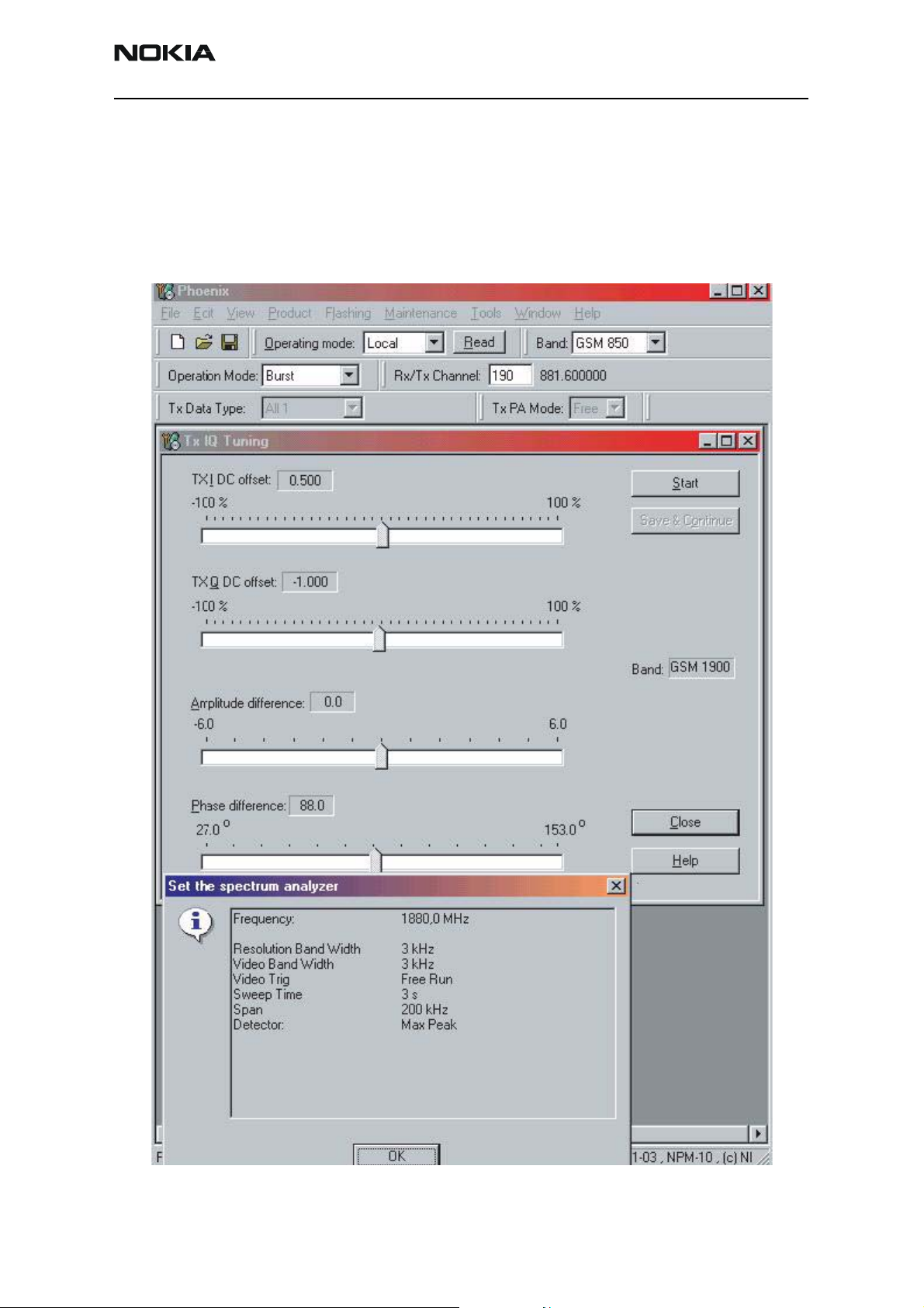
Use the following steps to tune the Tx I/Q:
1. Open the Maintenance menu, point to Tuning, and click Tx IQ Tuning.
2. Use the following spectrum analyzer settings for Tx I/Q tuning:
• Same center frequencies for GSM 850 (Ch190 = 836.6 MHz) and GSM 1900
(Ch661 = 1880 MHz) as in the Tx output power tuning
• Span = 200 kHz
•RBW = 10 kHz
Page 44 ©2004 Nokia Corporation Confidential Issue 2 03/2004
Page 45
NPM-10 (3595)
CC Technical Documentation Troubleshooting - RF
•VBW = 1 kHz
• Sweeptime = .5 seconds
• RF attenuation = 20 dB
• Reference level = 30 dBm
• Trigger = free run
3. Select where to get the values. Typically, you would click Load From Product.
4. Push the Start soft key.
5. Use the sliding arrows or the + and - keys to adjust the Tx I DC offset and Tx Q
DC offset values to reduce the carrier frequency to a minimum. The carrier must
be at least –30 dBc. Typically, carrier suppression is better than –40 dBc.
Figure 43: Tx IQ Tuning dialog box settings
Issue 2 03/2004 ©2004 Nokia Corporation Confidential Page 45
Page 46
NPM-10 (3595)
Troubleshooting - RF CC Technical Documentation
6. Use the sliding arrows or the + and - keys to adjust the Amplitude difference
and Phase difference values to reduce the lowest sideband frequency. The sideband must be reduced at least –35 dBc. Typically, sideband suppression is better
than -40 dBc.
7. Ensure that the IQ tuning values meet the specifications for both 1 and 0 data
types.
Figure 44: GSM 850 Tx IQ tuning values on the Set the spectrum analyzer message box
Page 46 ©2004 Nokia Corporation Confidential Issue 2 03/2004
Page 47
NPM-10 (3595)
CC Technical Documentation Troubleshooting - RF
8. Select the Save to Product box if you want to save the tuning values to the
phone.
9. Push the Stop soft key. This ends tuning and saves the values to the phone if you
have selected the Save to product box.
10. Repeat steps 1-11 for the PCS 1900 using channel 661. Figure 45 includes typical
tuning values for the PCS 1900.
Figure 45: PCS 1900 Tx IQ tuning values on the Set the spectrum analyzer message box
Issue 2 03/2004 ©2004 Nokia Corporation Confidential Page 47
Page 48

NPM-10 (3595)
Troubleshooting - RF CC Technical Documentation
RF Control
Use the following steps to check the receiver or transmitter without going in a call. This
process is similar to a call, but you have control through the PC instead of the tester.
Ensure that the GSM 850 Tx PA mode is set to High.
1. Open the Maintenance menu, point to Testing, and click RF Controls.
2. If you want to tune at other channels than the default, then you must select the
channels first in RF control and then start the tuning.
Call Testing
A call is the ultimate test of the phone if the tunings are complete and the phone’s Tx
and Rx are working properly. Use the following steps to manually test the phone with a
call:
1. Set the communications tester to manual test.
2. Switch the phone to Normal if it was in Local Mode. Remember to have a test
3. A call can be made after the phone has registered to the communications tester.
4. In the Autocaller (Maintenance Testing) you can answer by ticking Answer when
Figure 46: RF Controls dialog box
simcard in the phone.
It is possible to let the phone answer via Phoenix.
button pushed and then push the button.
Page 48 ©2004 Nokia Corporation Confidential Issue 2 03/2004
 Loading...