

Page 1

PAMS Technical Documentation
NHM-8NX Series Transceivers
System Module & UI
Issue 1 05/02 ãNokia Corporation
Page 2

NHM-8NX
System Module & UI PAMS Technical Documentation
Table of Contents
Abbreviations ................................................................................................................. 4
Transceiver NHM-8NX - Baseband Module BF4A ...................................................... 5
Hardware characteristics in brief .................................................................................5
Technical Summary .....................................................................................................6
Technical Specifications ..............................................................................................7
Operating conditions ................................................................................................. 7
DC Characteristics.................................................................................................... 8
Internal Signals and Connections.............................................................................. 9
Current consumption during sleep .......................................................................... 15
External Signals and Connections........................................................................... 16
Functional Description ...............................................................................................18
Modes of Operation................................................................................................. 18
Charging ................................................................................................................. 21
Charging Circuitry Electrical Characteristics ......................................................... 23
Power Up and Reset ................................................................................................ 24
A/D Channels .......................................................................................................... 26
LCD & Keyboard Backlight ................................................................................... 28
LCD cell .................................................................................................................. 29
SIM Interface........................................................................................................... 31
Internal Audio ......................................................................................................... 32
Accessories.............................................................................................................. 35
Keyboard ................................................................................................................. 40
RF Interface Block .................................................................................................. 41
Memory Module...................................................................................................... 42
Flash Programming ................................................................................................. 54
EMC Strategy ............................................................................................................57
PWB strategy........................................................................................................... 57
LCD metal frame..................................................................................................... 59
Bottom connector .................................................................................................... 59
Mechanical shielding............................................................................................... 60
Security ......................................................................................................................60
Test Interfaces ............................................................................................................60
Production / After Sales Interface ........................................................................... 60
FLASH Interface ..................................................................................................... 61
FBUS Interface........................................................................................................ 61
MBUS Interface ...................................................................................................... 61
JTAG & Ostrich Interface ....................................................................................... 62
DAI.......................................................................................................................... 62
Test modes (SW dependant) ................................................................................... 62
Test points ............................................................................................................... 63
List of unused UEM pins ..........................................................................................64
List of unused UPP pins ............................................................................................65
Transceiver NHM-8NX - RF Module.......................................................................... 67
Main Technical specifications ...................................................................................68
Temperature conditions........................................................................................... 68
Nominal and maximum ratings ............................................................................... 68
Page 2 ãNokia Corporation Issue 1 05/02
Page 3

NHM-8NX
PAMS Technical Documentation System Module & UI
RF frequency plan ................................................................................................... 68
DC characteristics ................................................................................................... 68
Functional descriptions ..............................................................................................71
RF block diagram .................................................................................................... 71
Frequency synthesizers ........................................................................................... 71
Receiver................................................................................................................... 73
Transmitter .............................................................................................................. 75
Synthesizer and RF Control .................................................................................... 76
RF characteristics .......................................................................................................77
Channel numbers and frequencies........................................................................... 77
Main RF characteristics........................................................................................... 77
Transmitter characteristics ...................................................................................... 77
Receiver characteristics........................................................................................... 81
List of Figures
Page No
Fig 1 NHM-8NX baseband block diagram..........................................................................6
Fig 2 UEM charging circuitry..............................................................................................21
Fig 3 Shared LED driver circuit for LCD and Keyboard backlight ....................................29
Fig 4 Complete overview of LCD module ..........................................................................29
Fig 5 BW4 LCD module......................................................................................................30
Fig 6 BSI Detection .............................................................................................................31
Fig 7 UEM & UPP SIM connections...................................................................................32
Fig 8 Speaker Interface ........................................................................................................33
Fig 9 Internal microphone electrical interface .....................................................................34
Fig 10 Interface between the MIDI-circuit and the UEM....................................................35
Fig 11 Mechanical layout and interconnections of DCT-4 battery......................................36
Fig 12 Headset interface ......................................................................................................37
Fig 13 DC-OUT Interface....................................................................................................39
Fig 14 Keyboard layout .......................................................................................................40
Fig 15 Intel-AMD signal deviations description .................................................................45
Fig 16 An XOR comparison of the data indicates more equal bits .....................................46
Fig 17 An XOR comparison indicates more unequal bits ...................................................46
Fig 18 Intel Asynchronous Read .........................................................................................50
Fig 19 Intel Synchronous Four-Word Burst Read ...............................................................51
Fig 20 Intel Write.................................................................................................................52
Fig 21 AMD Asynchronous Read .......................................................................................53
Fig 22 AMD Synchronous Burst Read ................................................................................53
Fig 23 Production/Test/After sales interface .......................................................................60
Fig 24 RF Frequency plan ...................................................................................................68
Fig 25 Power distribution diagram ......................................................................................70
Fig 26 Block Schematic.......................................................................................................71
Fig 27 Simplified Synthesizer..............................................................................................73
Fig 28 Simplified Mjoelner BB, either I or Q channel ........................................................73
Fig 29 Gain control ..............................................................................................................74
Fig 30 DC compensation principle ......................................................................................75
Fig 31 Power Loop ..............................................................................................................76
Issue 1 05/02 ãNokia Corporation Page 3
Page 4

NHM-8NX
System Module & UI PAMS Technical Documentation
Abbreviations
BSI Battery Size Indicator
CTI Cover Type Indicator
DCT4 Digital Core Technology, 4th Generation
DSP Digital Signal Processor
MCU MicroController Unit
NO_SUPPLY UEM state where UEM has no supply what so ever
PDM Pulse Density Modulation
PWR_OFF UEM state where phone is off
PWRONX Signal from power on key. '1' = key
RESET UEM state where regulators are enabled
RTC UEM internal Real Time Clock
SIM Subscriber Identity Module
SLEEP UEM power saving state controlled by UPP
SLEEPX SLEEP control signal from UPP
TBSF Through the Board Side Firing
UEM Universal Energy Management
UPP Universal Phone Processor
VBAT Main battery voltage
VBAT LIM2+ Charging cut–off limit (Max)
VCHAR Charger input voltage
VCHARDET Charger detection threshold level
VMSTR+, VMSTR Master Reset threshold level (2.1 V / 1.9 V)
Page 4 ãNokia Corporation Issue 1 05/02
Page 5

NHM-8NX
PAMS Technical Documentation System Module & UI
Transceiver NHM-8NX - Baseband Module BF4A
This section specifies the baseband module for the NHM-8NX transceiver. The transceiver
board is named BF4A, and all board references used refer to the board version BF4A_20.
The baseband module includes the baseband engine chipset, the UI components and the
acoustical parts for the transceiver.
NHM-8NX is a hand-portable dualband EGSM900/GSM1800 phone, with GPRS (Class-4)
for the Basic/Expression segment, having the DCT4 generation baseband (UEM/UPP) and
RF(MJOELNER) circuitry.
The baseband module is developed, as part of the DCT4 common Baseband. It is based
very much upon the NPE-4 and NHM-7 products, main difference being UI and the audio
circuits.
The mechanical construction is based on the NHM-5 phone.
New features in NHM-8NX are MIDI (polyphonic ringing tones) and DC-out (electrical
interface to A-cover).
NHM-8NX supports both three and two wire type DCT3 chargers. Three wire chargers are
treated like two wire ones. There is no separate PWM output for controlling charger but
it is connected to GND inside the bottom connector.
BLC-2 Li-ion battery is used as main power source for NHM-8. BLC-2 has nominal
capacity of 900 mAh.
Hardware characteristics in brief
• Hi-Res (96x65) illuminated B&W display (BW4)
• Active LCD area: width 30,609mm, height 24.10 mm (pixel size
0.304mm*0.356mm, pixel gap 0,015)
• ESD-proof keymat, with 5 individual keys for multiple key pressing
• Support for internal semi-fixed batteries (Janette type)
• No RTC battery
• Plug-in SIM, supporting 1.8 & 3.0V
• Audio amplifier and SALT speaker for MIDI support
• Ringing volume 100dB @ 5cm (MIDI tones through SALT speaker)
• Internal vibra
• Supports voice dial activation via headset button
• DC-out feature for supporting electrical A-covers
• Only 4 (2+2) TBSF LEDs for keyboard & LCD backlight
• 6-layer PWB, only SMD components on one side
• Li-Ion is the only supported battery technology
Note: 5V SIM cards are no longer supported by DCT-4 generation baseband.
Issue 1 05/02 ãNokia Corporation Page 5
Page 6
NHM-8NX
System Module & UI PAMS Technical Documentation
Technical Summary
The baseband module contains 2 main ASICs named the UEM and UPP. The baseband
module furthermore contains an audio amplifier LM4890 for MIDI support and a 64Mbit
Flash IC. The baseband is based on the DCT4 engine program.
Figure 1: NHM-8NX baseband block diagram
RFBUS
Battery
UI
Mjoelner
PA S upply
RF Supplies
RF RX/TX
SIM
EAR
MIC
LM4890
VIBRA
M
UEM
HF
DCT4 Janette connector
External Audio
Charger connection
Baseband
DLIGHT
SLEEPCLK
32kHz
CBUS/
DBUS
BB
Supplies
MBus/FBus
26MHz
UPP
MEMADDA
FLASH
The UEM supplies both the baseband module as well as the RF module with a series of
voltage regulators. Both the RF and Baseband modules are supplied with regulated voltages of 2.78 V and 1.8V. UEM includes 6 linear LDO (low drop-out) regulators for baseband and 7 regulators for RF. BB regulator VFLASH1, RF regulators VR1B, VR4 as well as
the current sources IPA1 and IPA2 must be kept disabled by SW, as they are left unconnected on the PWB. The UEM is furthermore supplying the baseband SIM interface with a
programmable voltage of either 1.8 V or 3.0 V. The core of the UPP is supplied with a
programmable voltage of 1.0 V, 1.3 V, 1.5 V or 1.8 V.
UPP operates from a 26MHz clock, coming from the RF ASIC MJOELNER (see chapter 7.11
for details), the 26 MHz clock is internally divided by two, to the nominal system clock of
13MHz. DSP and MCU contain phase locked loop (PLL) clock multipliers, which can multiply the system frequency by factors from 0.25 to 31. Practical speed limitations is
depending on memory configuration and process size (Max. DSP speed for C035 process
is ~ 200MHz)
The UEM contains a real-time clock, sliced down from the 32768 Hz crystal oscillator.
Page 6 ãNokia Corporation Issue 1 05/02
Page 7
NHM-8NX
PAMS Technical Documentation System Module & UI
The 32768 Hz clock is fed to the UPP as a sleep clock.
The communication between the UEM and the UPP is done via the bi-directional serial
buses CBUS and DBUS. The CBUS is controlled by the MCU and operates at a speed of 1
MHz. The DBUS is controlled by the DSP and operates at a speed of 13 MHz. Both processors are located in the UPP.
The interface between the baseband and the RF section is mainly handled by the UEM
ASIC. UEM provides A/D and D/A conversion of the in-phase and quadrature receive and
transmit signal paths and also A/D and D/A conversions of received and transmitted
audio signals to and from the user interface. The UEM supplies the analog signals to RF
section according to the UPP DSP digital control. RF ASIC MJOELNER is controlled
through UPP RFBUS serial interface. There are also separate signals for PDM coded audio.
Digital speech processing is handled by the DSP inside UPP ASIC. UEM is a dual voltage
circuit, the digital parts are running from the baseband supply 1.8V and the analog parts
are running from the analog supply 2.78V also VBAT is directly used by some blocks.
The baseband supports both internal and external microphone inputs and speaker outputs. Input and output signal source selection and gain control is done by the UEM
according to control messages from the UPP. Keypad tones, DTMF, and other audio tones
are generated and encoded by the UPP and transmitted to the UEM for decoding. NHM8NX has two external serial control interfaces: FBUS and MBUS. These busses can be
accessed only through production test pattern as described in section Test Interfaces.
NHM-8NX transceiver module is implemented on 6 layer selective OSP/Gold coated PWB.
Technical Specifications
Operating conditions
Temperature Conditions
Table 1: Temperature conditions for NHM-8
Environmental condition Ambient temperature Remarks
Normal operation -25 ° C … +55 °C Specifications fulfilled
Reduced performance -40 °C ..-25 °C
and +55 °C … +85 °C
No operation and/or storage < -40 °C or > +85 °C No storage or operation. An attempt to
operate may damage the phone permanently
Absolute Maximum Ratings
Table 2: Absolute Maximum Ratings
Signal Rating
Battery Voltage -0.3 ... 5.4V (VBAT LIM2H+))
Issue 1 05/02 ãNokia Corporation Page 7
Page 8
NHM-8NX
System Module & UI PAMS Technical Documentation
Charger Input Voltage -0.3 ... 20V
DC Characteristics
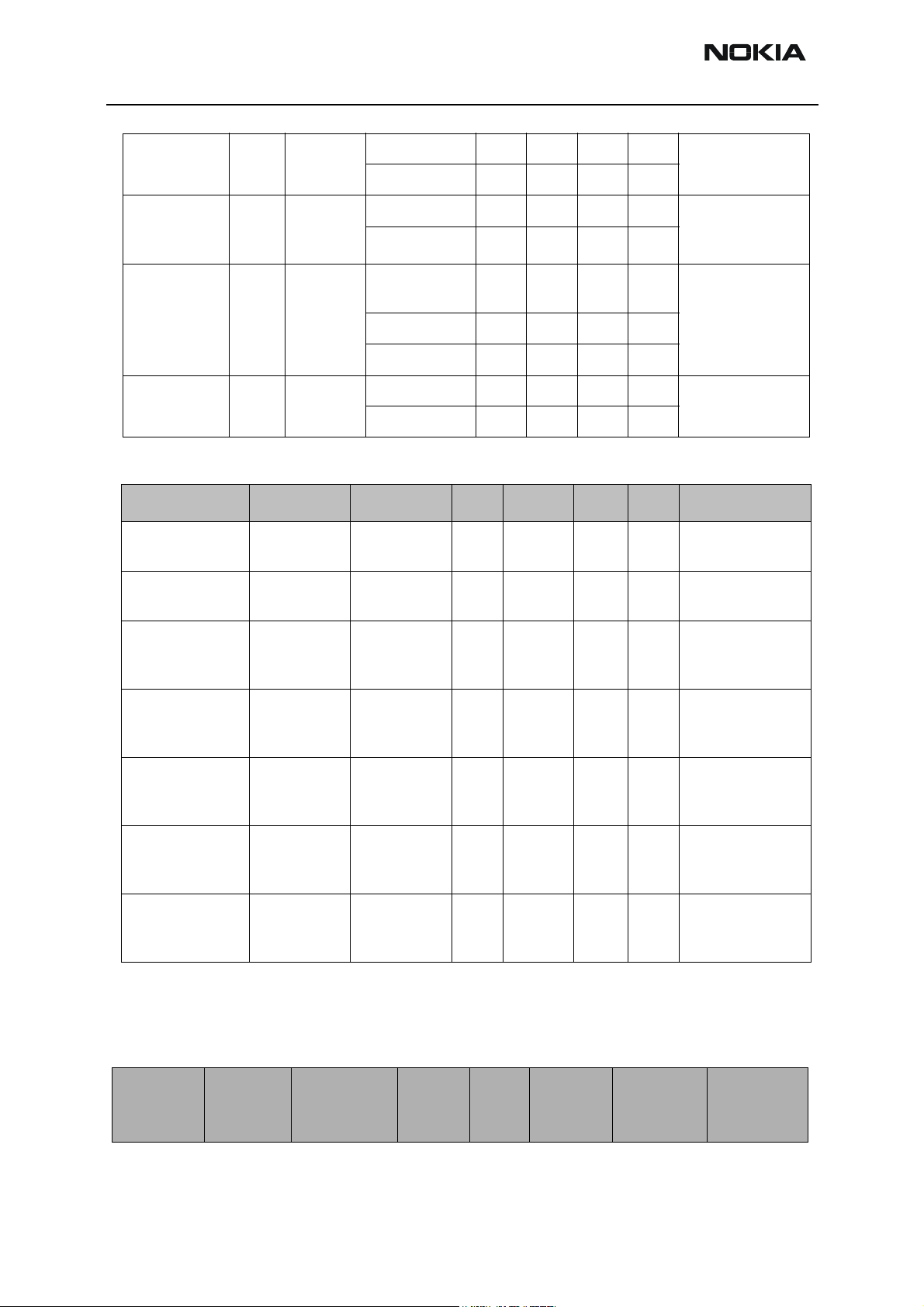
Regulators and Supply Voltage Ranges
Table 3: Battery voltage range
Signal Min Nom Max Note
VBAT 3.1V 3.6V 4.235V 3.1V SW cut off
Table 4: BB regulators
Signal Min Nom Max Note
VANA 2.70V 2.78V 2.86V I
VFLASH1 2.70V 2.78V 2.86V I
max
max
I
Sleep
= 80mA
= 70mA
= 1.5mA
VFLASH2 2.70V 2.78V 2.86V Not used
VSIM 1.745V
2.91V
VIO 1.72V 1.8V 1.88V I
VCORE 1.0V
1.235V
1.425V
1.710V
1.8V
3.0V
1.053V
1.3V
1.5V
1.8V
1.855V
3.09V
1.106V
1.365V
1.575V
1.890V
I
= 25mA
max
= 0.5mA
I
Sleep
= 150mA
max
I
= 0.5mA
Sleep
I
= 200mA
max
= 0.2mA
I
Sleep
Used voltages:
(c05) = 1.8V
(c035) = 1.5V
Table 5: RF regulators
Signal Min Nom Max Note
VR1A 4.6V 4.75V 4.9V Imax = 10mA
VR1B 4.6V 4.75V 4.9V Not used
VR2 2.70V
3.20V
VR3 2.70V 2.78V 2.86V I
2.78V
3.3V
2.86V
3.40V
I
max
max
= 100mA
= 20mA
VR4 2.70V 2.78V 2.86V Not used
VR5 2.70V 2.78V 2.86V I
VR6 2.70V 2.78V 2.86V I
max
I
Sleep
max
I
Sleep
= 50mA
= 0.1mA
= 50mA
= 0.1mA
Page 8 ãNokia Corporation Issue 1 05/02
Page 9
NHM-8NX
PAMS Technical Documentation System Module & UI
VR7 2.70V 2.78V 2.86V I
Table 6: Current sources
Signal Min Nom Max Note
IPA1 and IPA2 0mA - 5mA Not used
max
Internal Signals and Connections
The tables below describe internal signals. The signal names can be found on the schematic for the bf4a PWB.
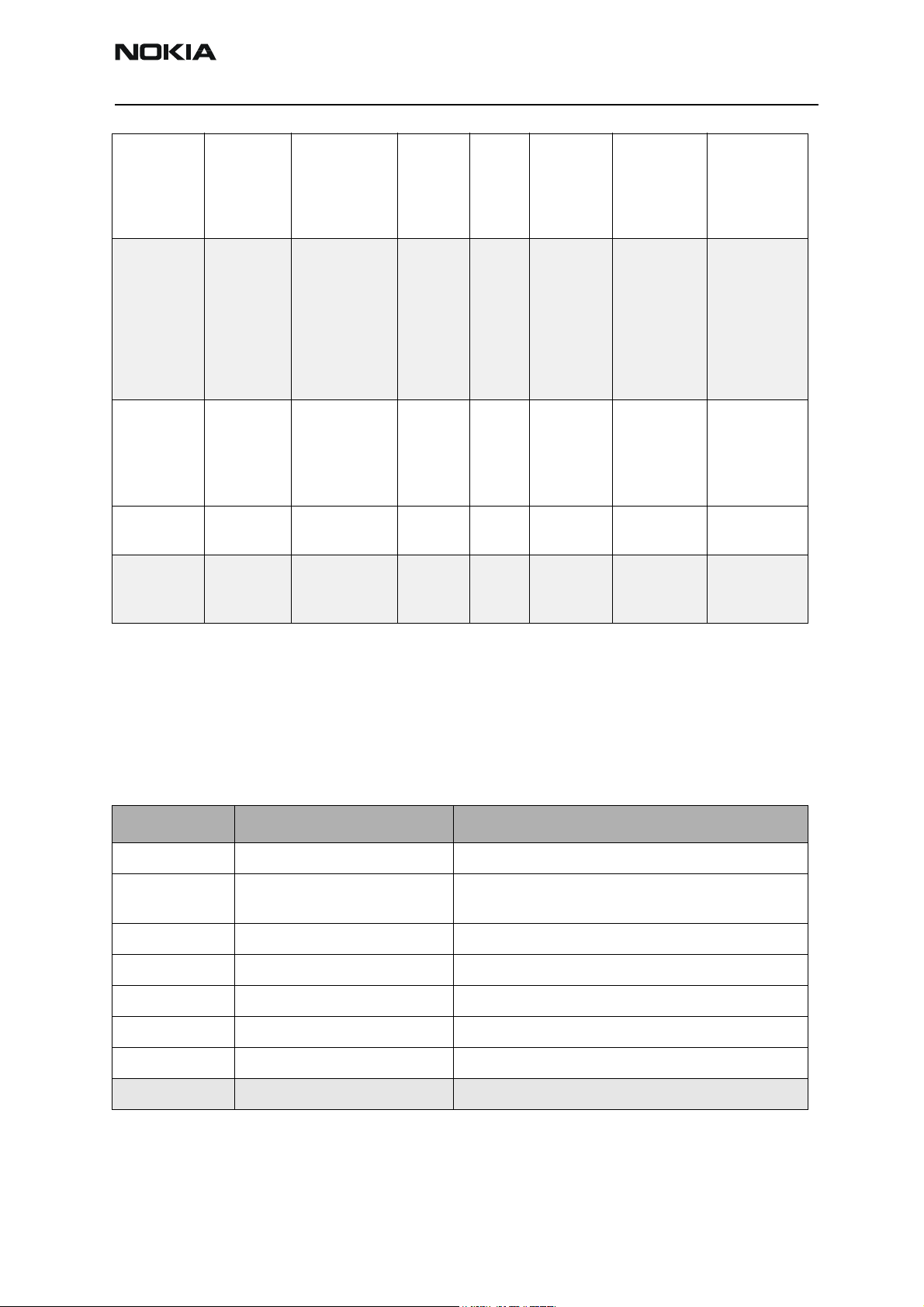
Audio
Table 7: Internal microphone
Signal Min Nom Max Condition Note
MIC1P (Differential input P) - - 100mV
MIC1N (Differential input N) - - 100mV
G=20dB 1kΩ to MIC1B
pp
G=20dB 1kΩ to GND
pp
(RC filtered by 220R/4.7uF)
= 45mA
MICB1 (Microphone Bias) 2.0 V 2.1 V 2.25 V DC
External loading of MICB1 - - 600uA DC
Table 8: Internal speaker (Differential output EARP & EARN)
Signal Min
Output voltage swing 4.0 - - Vpp Differential output
Load Resistance (EARP to EARN) 26 32 - W
Load Capacitance (EARP to EARN) - - 50 nF
No
Max Units Note
m
MIDI
Table 9: Connections between UPP and LM4890
Signal From To Parameter Min. Max. Unit Notes
Shutdown GENIO[14] Shutdown
(p. 5)
Vih
Vil
1.2
-
-
0.4
V
V
LM4890 detections treshold
levels
Table 10: Connections between UEM/Battery and LM4890
Signal name From To Parameter Min. Max. Unit Notes
Issue 1 05/02 ãNokia Corporation Page 9
Page 10
NHM-8NX
System Module & UI PAMS Technical Documentation
XAUDIO[1]
Filtered signal
UEM, HF No
direct con-
LM4890 Output Swing 1.0 - Vpp with 60 dB
nection
between
UEM and
LM4890
VBAT Battery LM4890
Supply 3.1 4.2 V Lower limit is
(p. 6)
LCD
Table 11: LCD connector interface
Pin Signal
NMP
net
Symbol Parameter Min.
1 /RES XRES Reset - - 0.3 x V
t
rw
1000 - - ns For valid reset
2 /SCE XCS Chip Select 0.7 x V
- - 0.3 x V
Ty
Max.
p.
- - V Logic High
DDI
Un
it
V Logic Low,
DDI
V Logic Low,
DDI
signal to total
distortion
ratio
SW cut-off
Notes
active
active
t
S2
t
H2
60 - - ns Setup time
100 - - ns Hold time
3 VSS VSS GND Ground - 0 - V
4 SDATA SDA Input 0.7 x V
- - 0.3 x V
Output @
I
= 0.5mA,
OL
I
= -
OH
0.7 x V
- - V Logic High
DDI
DDI
- - V Logic High
DDI
0.5mA
t
s1
t
H1
5 SCLK SCLK Serial clock
- - 0.3 x V
100 - - ns Data setup time
100 - - ns Data hold time
0.7 x V
- - V Logic High
DDI
DDI
input
- - 0.3 x V
t
cyc
153,8 - - ns Serial clock
DDI
V Logic Low
V Logic Low
V Logic Low
cycle (max. 4
MHz)
t
PWH1
50 - - ns Serial clock high
pulse width
Page 10 ãNokia Corporation Issue 1 05/02
Page 11
NHM-8NX
PAMS Technical Documentation System Module & UI
6 VDD
7 VDD
8 VLCD-
1
2in
out
t
PWL1
VDDI VDD digital
power supply
VDD Booster
power supply
VOUT Booster out-
put
50 - - ns Serial clock low
pulse width
1.72 1.8 1.88 V
2.6 2.782.86 V VFLASH1
- - 12 V Decoupled to
GND on PCB
with 1uF
Baseband – RF interface
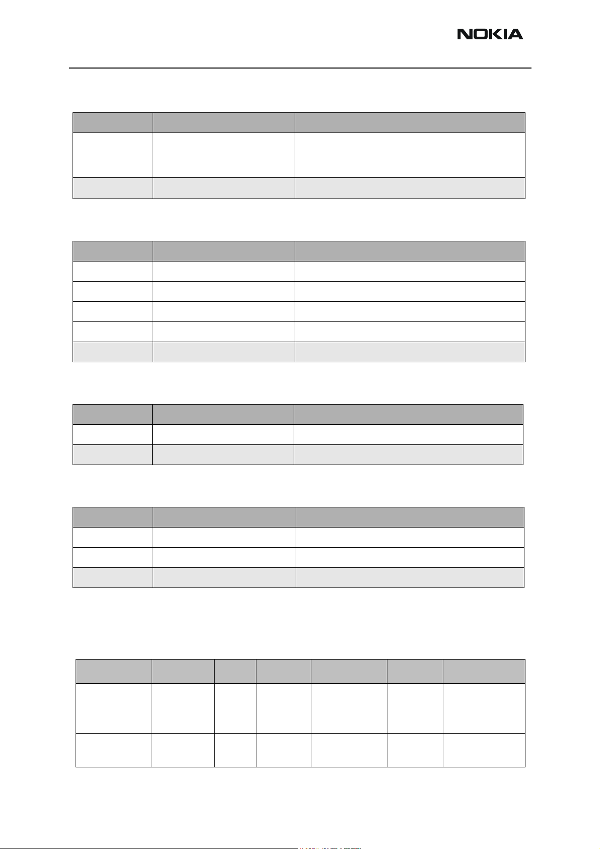
Table 12: BB – RF interface description
Signal name From To Parameter Min. Typ. Max. Unit Notes
RFICCNTRL (2:0) MJOELNER control bus
RFBUSEN1X UPP MJOEL-
NER
RFBUSDA UPP MJOEL-
NER
Logic "1" 1.38 - 1.80 V RF Chip select
Logic "0" 0 - 0.4 V
Logic "1" 1.38 - 1.80 V RF serial control
Logic "0" 0 - 0.4 V
bus (bi-directional)
RFBUSCLK UPP MJOEL-
NER
Clock System clock for phone
RFCLK MJOE
LNER
RFCONV (9:0) RF / BB analogue signals
RXIINP MJOE
LNER
UPP Frequency - 26 - MHz System clock
UEM Voltage swing 1.35 1.4 1.45 V Positive in-phase
Logic "1" 1.38 - 1.80 V RF bus clock
Logic "0" 0 - 0.4 V
Signal amplitude
Duty cycle
(Mjoelner
spec.)
DC level 1.3 1.35 1.4 V
I/Q amplitude
mismatch
I/Q phase mismatch
Data clock rate - - 13 MHz
0.3 1 1.376Vpp
40 - 60 %
- - 0.2 dB
-5 - 5 Deg.
UPP minimum
recommended
amplitude is
0.3Vpp.
Waveform: Sinus/
triangle
Rx signal
Issue 1 05/02 ãNokia Corporation Page 11
Page 12
NHM-8NX
System Module & UI PAMS Technical Documentation
RXIINN MJOE
LNER
RXQINP MJOE
LNER
RXQINN MJOE
LNER
UEM Voltage swing 1.35 1.4 1.45 V Negative in-phase
DC level 1.3 1.35 1.4 V
I/Q amplitude
mismatch
I/Q phase mismatch
Data clock rate - - 13 MHz
UEM Voltage swing 1.35 1.4 1.45 V Positive quadra-
DC level 1.3 1.35 1.4 V
I/Q amplitude
mismatch
I/Q phase mismatch
Data clock rate - - 13 MHz
UEM Voltage swing 1.35 1.4 1.45 V Negative quadra-
DC level 1.3 1.35 1.4 V
I/Q amplitude
mismatch
- - 0.2 DB
-5 - 5 Deg.
- - 0.2 dB
-5 - 5 Deg.
- - 0.2 dB
Rx signal
ture phase
nal
ture phase RX signal
RX sig-
TXIOUTP UEM MJOEL-
NER
TXIOUTN UEM MJOEL-
NER
I/Q phase mismatch
Data clock rate - - 13 MHz
Diff. Voltage
swing
DC level 1.10 1.20 1.25 V
Source impedance
Data clock rate - - 13 MHz
Differential
voltage swing
DC level 1.17 1.20 1.23 V
Source impedance
Data clock rate - - 13 MHz
-5 - 5 Deg.
2.15 2.2 2.25 Vpp Positive TX signal
- - 200 W
2.15 2.2 2.25 Vpp Negative TX sig-
- - 200 W
(program-able
voltage swing)
nal (program-able
voltage swing)
Page 12 ãNokia Corporation Issue 1 05/02
Page 13
NHM-8NX
PAMS Technical Documentation System Module & UI
TXQOUTP UEM MJOEL-
NER
TXQOUTN UEM MJOEL-
NER
GENIO (28:0) General purpose I/O
GENIO5
(TXP)
GENIO6
(RESETX_MJO
EL)
UPP MJOEL-
NER
UPP MJOEL-
NER
Differential
voltage swing
DC level 1.17 1.20 1.23 V
Source impedance
Data clock rate - - 13 MHz
Differential
voltage swing
DC level 1.17 1.20 1.23 V
Source impedance
Data clock rate - - 13 MHz
Logic "1" 1.38 - 1.80 V Transmitter power
Logic "0" 0 - 0.4 V
Logic "1" 1.38 - 1.80 V Reset to RF chip
Logic "0" 0 - 0.4 V
2.15 2.2 2.25 Vpp Positive TX signal
(program-able
voltage swing)
- - 200 W
2.15 2.2 2.25 Vpp Negative TX signal (program-able
voltage swing)
- - 200 W
control enable
RFAUXCONV(2:0) RF / BB analogue control signals
AUXOUT UEM MJOEL-
NER
Regulators RF regulators (currents are max. according to UEM spec.)
VBAT
(VBATREGS)
VR1A UEM Mjoelner Output voltage 4.6 4.75 4.9 V
VR2 UEM MJOEL-
VR3 UEM MJOEL-
Battery
PA / UEM Output voltage 2.9 3.6 4.2 V Battery cut-off is
NER
NER
Output voltage 0.12 - 2.50 V Transmitter power
Source impedance
Resolution - 10 - Bits
Current 0 - 10 mA
Output voltage 2.64 2.78 2.86 V Supply to:
Current 0.1 - 100 mA
Output voltage 2.64 2.78 2.86 V Supply to:
Current 0.1 - 20 mA
- - 200 W
control
set by UEM to 2.9
V
TX – chain, Power
Loop Control and
Digital logic
Ref. Osc.
VR5 UEM MJOEL-
NER
Output voltage 2.64 2.78 2.86 V Supply to:
Current 0.1 - 50 mA
PLL, Divider, LO
buffers
Issue 1 05/02 ãNokia Corporation Page 13
Page 14
NHM-8NX
System Module & UI PAMS Technical Documentation
VR6 UEM MJOEL-
NER
VR7 UEM VCO Output voltage 2.64 2.78 2.86 V Supply to:
VREFRF01 UEM MJOEL-
NER
VIO UEM MJOEL-
NER
Signal name From To Min. Typ. Max. Unit Notes
RFCLK MJOELNER UPP - 26 - MHz Active when
SLEEPCLK UEM UPP - 32.768 - kHz Active when VBAT
Output voltage 2.64 2.78 2.86 V Supply to:
Current 0.1 - 50 mA
Current 0.1 - 45 mA
Output voltage 1.3341.35 1.366V Used in MJOEL-
Current - - 100 µA
Current - - 100 µA
Output voltage 1.71 1.8 1.88 V Supply to:
Current 0.1 - 150 mA
Table 13: Board Clocks
LNA's, Pregain
LO buffers, Local
oscillators
NER (VBEXT) as
1.35V reference
BB buffer
SLEEPX is high
is supplied
RFCONVCLK UPP UEM 13 - MHz Active when RF
converters are
active
RFBUSCLK UPP MJOELNER - 13 13 MHz Only active when
bus-enable is
active
DBUSCLK UPP (DSP) UEM - 13 13 MHz Only active when
bus-enable is
active
CBUSCLK UPP (MCU) UEM - 1 1 MHz Only active when
bus-enable is
active
LCDCAMCLK UPP
(Write)
(Read)
LCD 0.3
3.25
0.650
4 MHz Only active when
bus-enable is
active
Connection for regulators active during sleep
Table 14: Connections for regulators active during sleep
Regulators UEM UPP FLASH LCD
X387
(SIM
con.)
MJOELNER
Externally
circuit
Page 14 ãNokia Corporation Issue 1 05/02
Page 15
NHM-8NX
PAMS Technical Documentation System Module & UI
VIO
[1,8V]
VCORE
[1,8V]
VFLASH1
[2,78V]
VSIM
[1,8V / 3V]
VR2
[2,78V]
VDD18 VDDIO1
VDDIO2
VDDIO3
VDDIO4
VDDA
VDDSP1
VDDSP2
VDDSP3
VDDMCU
VDDCORE1
VDDCORE2
VDDPDRAM1
VDDPDRAM2
VDD28
BSI(pull
up)
PATEMP
(pull up)
VDD VDDI VDDDL
SELADDR
VDD
VSIM
VDDDIG
VDDTX
TX section of
MJOELNER
sheet
Current consumption during sleep
Following section state the different regulators current consumption (theoretically
excluding leakage in decoupling capacitors) in sleep mode.
VIO
1,8V PINS Current consumption in sleep (SLEEPX = low)
UEM VDD18 < 5 µA
UPP VDDIO1-4 < 400uA
(depends on I/O config)
VDDA < 5uA
FLASH VDD 20 µA
LCD VDDI 40 µA
MJOELNER VDDDL 5 µA
SELADDR 0uA
Totally Specification: Max: 500uA <475
Issue 1 05/02 ãNokia Corporation Page 15
Page 16
NHM-8NX
System Module & UI PAMS Technical Documentation
VCORE
1,8V PINS Current consumption in sleep (SLEEPX = low)
UPP VDDSP1-3, VDDMCU,
VDDCORE1-2
VDDPDRAM1-2
To tal ly Specification: Max: 200uA Measured value < 120uA
< 9 µA
(Measured value < 120uA)
VFLASH1
2,78V PINS Current consumption in sleep (SLEEPX = low)
UEM VDD28 < 5 µA
BSI (pull up) < 30 µA
PATEMP (pull up) < 25 µA
LCD VDD <1100 µA
Totally Specification: Max: 1500uA <1160 µA
VSIM
1,8V / 3V PINS Current consumption in sleep (SLEEPX = low)
X387 (SIM con) VSIM < 200 µA
Totally Specification: Max: 500uA < 200 µA
VR2
2,78V PINS Current consumption in sleep (SLEEPX = low)
MJOELNER VDDDIG 70 µA
VDDTX 0 µA
Totally Specification: Max: 100uA 70uA
External Signals and Connections
System connector (X102)
Table 15: DC connector
Pin Signal Min Nom Max Condition Note
2 VCHAR - 11 .1 V
7.0
V
RMS
8.4 V
peak
RMS
16.9 V
7.9 V
1.0 A
9.2 V
850 mA
peak
RMS
peak
RMS
Standard
charger
(ACP-7)
Fast
charger
Charger positive
input
Page 16 ãNokia Corporation Issue 1 05/02
Page 17
NHM-8NX
PAMS Technical Documentation System Module & UI
1 CHGND - 0 - Charger ground
Table 16: External microphone
Signal Min Nom Max Condition Note
MIC2P (Differential input P) - - 100mV
MIC2N (Differential input N) - - 100mV
MICB2 (Microphone Bias) 2.0 V 2.1 V 2.25 V DC Unloaded
External loading of MICB2 - - 600uA DC
Table 17: External speaker, differential output XEARP(HF) & XEARN (HFCM)
Signal Min
Output voltage swing*
* seen from transducer side
Common voltage level for
HF output (HF & HFCM) VCMHF
Load Resistance (HF to HFCM) 30 - - W
Load Capacitance (HF to HFCM) - - 10 nF
2.0 - - Vpp Differential output, with 60 dB
0.75 0.8 0.85 V
Table 18: Headset detection
No
Max Units Note
m
G=20dB 1kΩ to MIC1B
pp
G=20dB 1kΩ to GND
pp
signal to total distortion ratio
Signal Min Nom Max Condition Note
HookInt 0V - 2.86V (VANA) Headset button call control, connected
to UEM AD-converter
HeadInt 0V - 2.86V (VANA) Accessory detection, connected to
UEM AD-converter
DC-OUT (J307,J308 & J309)
Table 19: DC-OUT Connections
Pad Name Parameter Min Typ Max Unit Notes
J307 Power Voltage (open) - - Vbat V Output power line
Current (short) 56 64 72 mA
J308 CTI(Input) Resistor value 30.9 - 750 kΩ Cover detection
J309 GND - - - - - Ground
SIM (X387)
Issue 1 05/02 ãNokia Corporation Page 17
Page 18
NHM-8NX
System Module & UI PAMS Technical Documentation
Table 20: SIM Connector
Pin Name Parameter Min Typ Max Unit Notes
1 CLK Frequency - 3.25 - MHz SIM clock
Trise/Tfall - - 50 ns
2 RST 1.8V SIM
Card
3V SIM
Card
3 VCC 1.8V SIM
Card
3V SIM
Card
4 GND GND - 0 - V Ground
5 VCC - - - Not con-
6 I/O 1.8V Voh
1.8V Vol
3 Voh
3 Vol
1.8V Vih
1.8V Vil
3V Vil
3V Vil
1.62
0
2.7
0
1.6 1.8 2.0 V Supply
2.8 3.0 3.2 V
1.62
0
2.7
0
1.26
0
2.1
0
”1”
”0”
”1”
”0”
”1”
”0”
”1”
”0”
”1”
”0”
”1”
”0”
VSIM
0.27
VSIM
0.45
VSIM
0.27
VSIM
0.45
VSIM
0.27
VSIM
0.45
V SIM reset
(output)
V
voltage
nected
V SIM data
(output)
V
V SIM data
(input)
V
Trise/Tfall
max 1us
Functional Description
Modes of Operation
NHM-8NX baseband engine has six different operating modes (in normal mode):
• No supply
•Power_off
•Acting Dead
•Active
•Sleep
• Charging
Additionally two modes exist for product verification: 'testmode' and 'local mode'.
No supply
In NO_SUPPLY mode, the phone has no supply voltage. This mode is due to disconnection
of main battery or low battery voltage level.
Page 18 ãNokia Corporation Issue 1 05/02
Page 19
NHM-8NX
PAMS Technical Documentation System Module & UI
Phone is exiting from NO_SUPPLY mode when sufficient battery voltage level is detected.
Battery voltage can rise either by connecting a new battery with VBAT > V
connecting charger and charging the battery above V
Power_off
MSTR+
.
MSTR+
or by
In this state the phone is powered off, but supplied. VRTC regulator is active (enabled)
having supply voltage from main battery. Note, the RTC status in PWR_OFF mode
depends on whether RTC was enabled or not when entering PWR_OFF. From Power_off
mode UEM enters RESET mode (after 20ms delay), if any of following statements is true
(logical OR –function):
• Power_on button detected (PWROFFX)
• Charger connection detected (VCHARDET)
• RTC_ALARM detected
The Phone enters POWER_OFF mode from all the other modes except NO_SUPPLY if
internal watchdog elapses.
Acting Dead
If the phone is off when the charger is connected, the phone is powered on but enters a
state called ”Acting Dead”, in this mode no RF parts are powered. To the user, the phone
acts as if it was switched off. A battery charging alert is given and/or a battery charging
indication on the display is shown to acknowledge the user that the battery is being
charged.
Active
In the active mode the phone is in normal operation, scanning for channels, listening to
a base station, transmitting and processing information. There are several sub-states in
the active mode depending on if the phone is in burst reception, burst transmission, if
DSP is working etc.
In active mode the RF regulators are controlled by SW writing into UEM’s registers
wanted settings: VR1A/B must be kept disabled. VR2 can be enabled or forced into low
quiescent current mode. VR3 is always enabled in active mode. VR4 -VR7 can be enabled,
disabled or forced into low quiescent current mode.
Table 21: Regulator controls
Regulator NOTE
VFLASH1 Enabled; Low Iq mode during sleep
VFLASH2 Not used in NHM-8, must be kept disabled
VANA Enabled; Disabled in sleep mode
Issue 1 05/02 ãNokia Corporation Page 19
Page 20
NHM-8NX
System Module & UI PAMS Technical Documentation
VIO Enabled; Low Iq mode during sleep
VCORE Enabled; Low Iq mode during sleep
VSIM Controlled by register writing.
VR1A Enabled; Disabled in sleep mode
VR1B Not used in NHM-8, must be kept disabled
VR2 Controlled by register writing; Enabled in sleep mode
VR3 Enabled; Disabled in sleep mode
VR4 Not used in NHM-8, must be kept disabled
VR5 Enabled; Disabled in sleep mode
VR6 Enabled; Disabled in sleep mode
VR7 Enabled; Disabled in sleep mode
IPA1-2 Not used in NHM-8, must be kept disabled
Sleep mode
Sleep mode is entered when both MCU and DSP are in stand-by mode. Sleep is controlled
by both processors. When SLEEPX low signal is detected UEM enters SLEEP mode. VCORE,
VIO and VFLASH1 regulators are put into low quiescent current mode. All RF regulators,
except VR2, are disabled in SLEEP. When SLEEPX=1 is detected UEM enters ACTIVE mode
and all functions are activated.
The sleep mode is exited either by the expiration of a sleep clock counter in the UEM or
by some external interrupt, generated by a charger connection, key press, headset connection etc.
In sleep mode the main oscillator (26MHz) is shut down and the 32 kHz sleep clock oscillator is used as reference clock for the baseband.
Charging
Charging can be performed in parallel with any other operating mode. A BSI resistor
inside the battery pack indicates the battery type/size. The resistor value corresponds to
a specific battery capacity and technology.
The battery voltage, temperature, size and current are measured by the UEM controlled
by the charging software running in the UPP.
The charging control circuitry (CHACON) inside the UEM controls the charging current
delivered from the charger to the battery. The battery voltage rise is limited by turning
the UEM switch off when the battery voltage has reached VBATLim (programmable
charging cut-off limits 3.6V / 5.0V / 5.25V). Charging current is monitored by measuring
the voltage drop across a 220 mOhm resistor. Detailed description of the charging func-
Page 20 ãNokia Corporation Issue 1 05/02
Page 21
NHM-8NX
V
PAMS Technical Documentation System Module & UI
tionality can be found in next section.
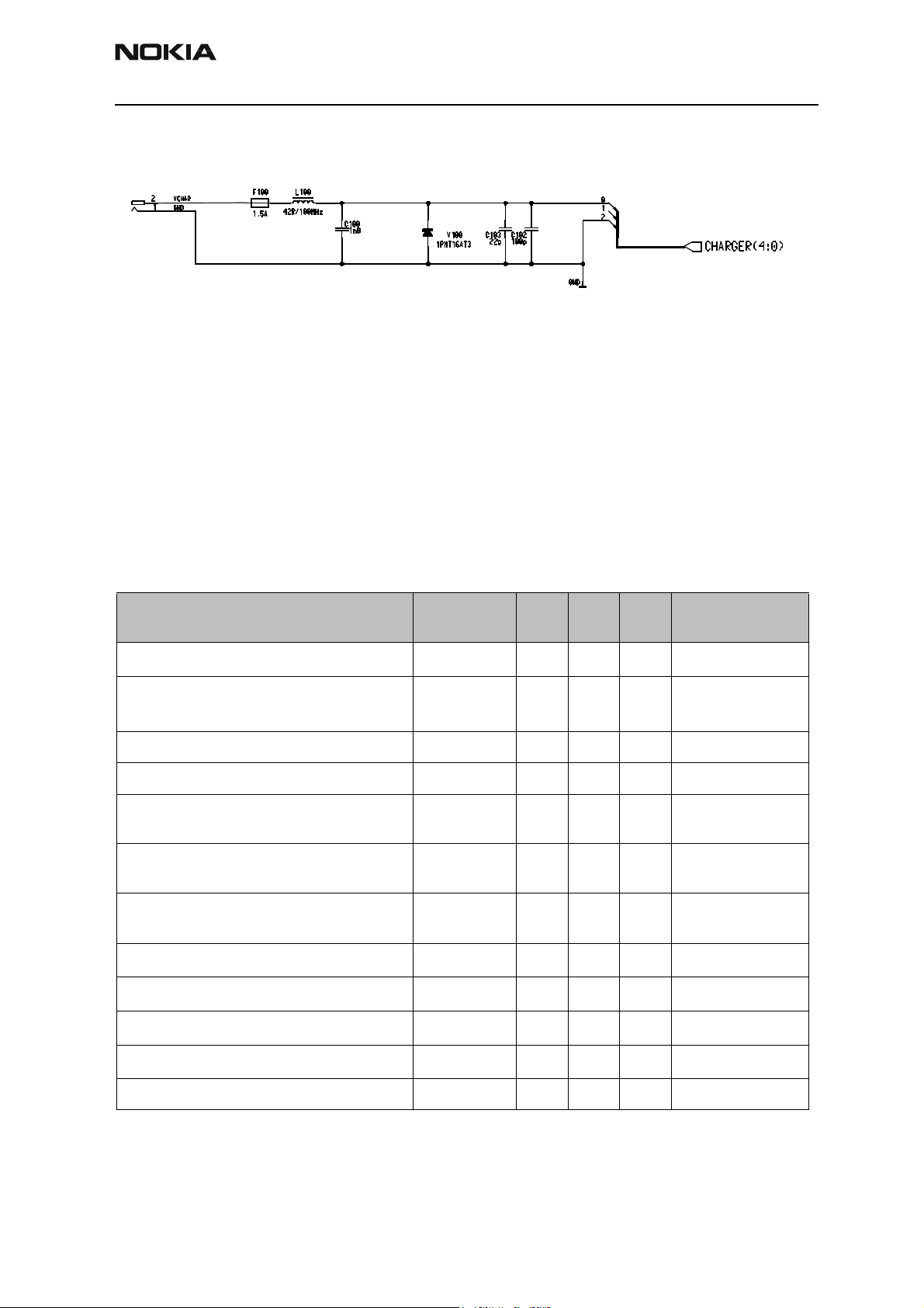
Charging
NHM-8NX supports the NMP Janette Charger interface.
Charging is controlled by the UEM ASIC, and external components are mounted for EMC,
reverse polarity and transient protection of the input to the baseband module. The
charger connection is through the system connector interface. Both 2- and 3-wire type
chargers are supported.
The operation of the charging circuit has been specified in such a way as to limit the
power dissipation across the charge switch and to ensure safe operation in all modes.
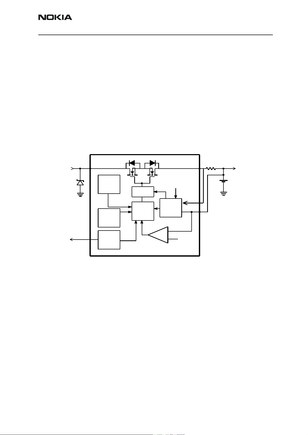
Figure 2: UEM charging circuitry
UEM
CHAR
PWM
VCHARin
Over
Temp.
Detection
WatchDog
PWM
Generator
Switch
Driver
Ctrl
Logic
Comp
Vmstr
Current
Sensing/
Limit
+
-
VCHARout
VBATT
VB ATT lim
VBATT
Charger Detection
Connecting a charger creates voltage on VCHAR input of the UEM. When VCHAR input
voltage level is detected to rise above VCH
threshold by UEM charging starts.
DET+
VCHARDET signal is generated to indicate the presence of the charger for the SW.
The charger identification/acceptance is controlled by EM SW.
The charger recognition is initiated when the EM SW receives a ”charger connected”
interrupt. The algorithm basically consists of the following three steps:
1. Check that the charger output (voltage and current) is within safety limits.
2. Identify the charger.
3. Check that the charger is within the charger window.
If the charger is accepted and identified, the appropriate charging algorithm is initiated.
Issue 1 05/02 ãNokia Corporation Page 21
Page 22

NHM-8NX
System Module & UI PAMS Technical Documentation
Charge Control
In active mode charging is controlled by UEM’s digital part. Charging voltage and current
monitoring is used to limit charge into safe area. For that reason UEM has programmable
charging cut-off limits VBATLim
(3.6V / 5.0V / 5.25V). Maximum charging current
1,2L,2H
is limited to 1.2 A. Default for VBATLim is 3.6V (used for Initial charging of empty battery).
VBATLim
VBATLim
are designed with hysteresis. When the voltage rises above
1,2L,2H
+ charging is stopped by turning charging switch OFF. No change in oper-
1,2L,2H
ational mode is done. After voltage has decreased below VBATLim- charging re-starts.
If VBAT is detected to rise above the programmed limit, the output signal OVV is set to ‘1’
by CHACON. If charging current limit is reached OVC output is set ‘1’ by CHACON.
Pulse-width-Modulated (PWM) control signals PWM1 and PWM32 are generated by
UEM’s digital part to CHACON block.
In principle there are two PWM frequencies in use depending on the type of the charger
(standard charger 1Hz, fast charger 32Hz. Duty cycle range is 0% to 100%), but in NHM8NX only the 1Hz mode will be used, as all charger will be treated as standard charges
(2-wire types).
Supported Chargers
Supported chargers are:
• 2-wire chargers: ACP-7, ACP-8 and ACP-12.
• 3-wire chargers: PPH-1, ACP-9,, ACT-1, LCH-8 and LCH-9.
The 3-wire chargers have a 3 wire interface to the phone, 2 power and 1 control. The
control wire carries the 32Hz digital pulse width modulated signal which must be generated by the phone to control the charger output voltage. In NHM-8NX the 32Hz PWM
for the charger is connected to GND inside the bottom connector. This sets full charger
output voltage and equals 0% PWM from charger point of view.
Charger Interface Protection
In order to ensure safe operation with all chargers and in misuse/fail situations charger
interface is protected using transient voltage suppressor (TVS) and 1.5A fuse. TVS used in
NHM-8NX is 16V@175W device.
Page 22 ãNokia Corporation Issue 1 05/02
Page 23
NHM-8NX
PAMS Technical Documentation System Module & UI
Table 22: Charger interface
TVS characteristics:
Breakdown voltage (V
Reverse standoff voltage (V
Max reverse leakage current at V
Max peak impulse current (I
Max clamping voltage at I
) 17.8Vmin (at IT 1.0mA)
BR
) 16V
R
(IR) 5uA
R
) 7A (at Ta=25*C, current waveform: 10/1000us)
pp
(Vc) 26V
pp
Charging Circuitry Electrical Characteristics
Table 23: Electrical Characteristics
Parameter
Test conditions
Input voltage range (fast charger, no load) VCHAR 7.0 8.4 9.2 V
Input voltage range (std charger, no load) - 11 .1
Absolute Maximum VCHAR voltage -0.3 - +20 V
Input resistance from VCharIn to ground Rin 2 4 6 kΩ
Master reset threshold level
VCOFFX threshold levels
VCHAR detection threshold level
Continuous input current (fast charger) I
Symbol Min Typ Max Units
16.9 V
7.9
V
MSTR+
VMSTR-
V
COFF+
VCOFF-
VCH
DET+
VCHDET-
CH
2.0
1.8
3.0
2.7
1.9
1.7
2.1
1.9
3.1
2.8
2.0
1.8
2.2
2.0
3.2
2.9
2.1
1.9
- - 850 mA
V
V
V
V
RMS
peak
RMS
Maximum input current (std charger) I
Start-up mode charging current I
PWM mode charge current I
CH
START
LIM
- - 1.0 A
100 - 150 mA
1.1 1.2 1.45 A
peak
Output voltage (Battery voltage) VBAT 0 3.6 4.2 V
Issue 1 05/02 ãNokia Corporation Page 23
Page 24
NHM-8NX
System Module & UI PAMS Technical Documentation
Charging cut-off limits (programmable) VBATLim
VBATLim1VBATLim2L+
VBATLim2LVBATLim2H+
VBATLim2H-
Charging switch resistance
(includes bonding and leads)
Temp =65°C (ambient)
PWM frequency (std charger) 0.5 1 1.5 Hz
PWM duty cycle 0 - 100 %
Switch output current slew rate SR 0.4 0.6 0.8 A/ms
Charging thermal shutdown threshold TjsdC+
VFLASH1 supply voltage input VFLASH1 2.7 2.78 2.88 V
R
TjsdC-
1+
SW
3.54
3.32
4.85
4.65
5.10
4.90
- - 0.3 W
140
120
3.65
3.50
5.0
4.85
5.25
5.10
150
130
3.76
3.66
5.15
5.05
5.40
5.30
160
140
Note: VCHAR is used as a supply voltage for charging control parts
Power Up and Reset
Power up and reset is controlled by the UEM ASIC. NHM-8NX baseband can be powered
up in following ways:
V
°C
1 Press power button, which means grounding the PWRONX pin of the UEM
2 Connect the charger to the charger input
3 Supply battery voltage to the battery pin
4 RTC Alarm, the RTC has been programmed to give an alarm
After receiving one of the above signals, the UEM counts a 20ms delay and then enters
it’s reset mode. The watchdog starts up, and if the battery voltage is greater than Vcoff+
a 200ms delay is started to allow references etc. to settle. After this delay elapses the
VFLASH1 regulator is enabled. 500us later VR3, VANA, VIO and VCORE are enabled.
Finally the PURX line is held low for 20 ms. This reset, PURX, is fed to the baseband ASIC
UPP, resets are generated for the DSP and the MCU. During this reset phase the UEM
forces the VCXO regulator on regardless of the status of the sleep control input signal to
the UEM. All baseband regulators are switched on at the UEM power on except for the
SIM regulator that is controlled by the MCU. The UEM internal watchdog is running during the UEM reset state, with the longest watchdog time selected. If the watchdog
expires the UEM returns to power off state. The UEM watchdog is internally acknowledged at the rising edge of the PURX signal in order to always give the same watchdog
response time to the MCU.
Power up with PWR key
When the Power on key is pressed the UEM enters the power up sequence as described in
Page 24 ãNokia Corporation Issue 1 05/02
Page 25

NHM-8NX
PAMS Technical Documentation System Module & UI
the section Power Up and Reset. Pressing the power key causes the PWRONX pin on the
UEM to be grounded. The UEM PWRONX signal is not part of the keypad matrix. The
power key is only connected to the UEM. This means that when pressing the power key
an interrupt is generated to the UPP that starts the MCU. The MCU then reads the UEM
interrupt register and notice that it is a PWRONX interrupt. The MCU now reads the status of the PWRONX signal using the UEM control bus, CBUS. If the PWRONX signal stay
low for a certain time the MCU accepts this as a valid power on state and continues with
the SW initialization of the baseband. If the power on key does not indicate a valid
power on situation the MCU powers off the baseband.
Power up when charger is connected
In order to be able to detect and start charging in a case where the main battery is fully
discharged (empty) and hence UEM has no supply (NO_SUPPLY mode of UEM) charging
is controlled by START-UP CHARGING circuitry.
Whenever VBAT level is detected to be below master reset threshold (V
MSTR-
) charging is
controlled by START_UP charge circuitry. Connecting a charger forces VCHAR input to
rise above charger detection threshold, VCH
. By detection start-up charging is
DET+
started. UEM generates 100mA constant output current from the connected charger’s
output voltage. As battery charges its voltage rises, and when VBAT voltage level higher
than master reset threshold limit (V
) is detected START_UP charge is terminated.
MSTR+
Monitoring the VBAT voltage level is done by charge control block (CHACON). MSTRX=‘1’
output reset signal (internal to UEM) is given to UEM’s RESET block when VBAT>V
MSTR+
and UEM enters into the reset sequence described in section Power Up and Reset.
If VBAT is detected to fall below V
during start-up charging, charging is cancelled.
MSTR-
It will restart if new rising edge on VCHAR input is detected (VCHAR rising above VCH-
).
DET+
Power up when battery is connected
Baseband can be powered up by connecting battery with sufficient voltage. Battery voltage has to be over UEM internal comparator threshold level, V
. Battery low limit is
coff+
specified in Table 2. When battery proper voltage is detected UEM enters to reset
sequence as described in section Power Up and Reset. This power up sequence is meant
for test purposes, in normal use (Btemp resistor > 1kΩ) the phone will power off again
immediately, without noticing the user.
RTC alarm power up
If phone is in POWER_OFF mode when RTC alarm occurs the wake up procedure is as
described in section Power Up and Reset. After baseband is powered on an interrupt is
given to MCU. When RTC alarm occurs during ACTIVE mode the interrupt for MCU is
generated.
Issue 1 05/02 ãNokia Corporation Page 25
Page 26
NHM-8NX
System Module & UI PAMS Technical Documentation
A/D Channels
The UEM contains the following A/D converter channels that are used for several measurement purposes. The general slow A/D converter is a 10 bit converter using the UEM
interface clock for the conversion. An interrupt will be given at the end of the measurement.
The UEM’s 11-channel analog to digital converter is used to monitor charging functions,
battery functions, voltage levels in external accessory detection inputs, user interface
and RF functions.
When the conversion is started the converter input is selected. Then the signal processing block creates a data with MSB set to ’1’ and others to ’0’. In the D/A converter this
data controls the switches which connect the input reference voltage (VrefADC) to the
resistor network. The generated output voltage is compared with the input voltage under
measurement and if the latter is greater, MSB remains ’1’ else it is set ’0’. The following
step is to test the next bit and the next., until LSB is reached. The result is then stored to
ADCR register for UPP to read.
The monitored battery functions are battery voltage (VBATADC), battery type (BSI) and
battery temperature (BTEMP) indication.
The battery type is recognized through a resistive voltage divider. In phone there is a
100kOhm pull up resistor in the BSI line and the battery has a pull down resistor in the
same line. Depending on the battery type the pull down resistor value is changed. The
battery temperature is measured equivalently except that the battery has a NTC pull
down resistor in the BTEMP line.
KEYB1&2 inputs are made for keyboard scanning purposes. These inputs are also routed
internally to the miscellaneous block. KEYB1&2 inputs are not used In NHM-8, and the
connected interrupts must be kept disabled by SW.
The HEADINT and HOOKINT are external accessory detection inputs used for monitoring
voltage levels in these inputs. They are routed internally from the miscellaneous block
and they are connected to the converter through a 2:1 multiplexer.
PATEMP and VCXOTEMP channels are not used as originally intended. PATEMP input is
used for detection of accessory covers (CTI), VCXOTEMP is not used in NHM-8.
Table 24: Slow A/D converter characteristics
Characteristics Min Typ Max Unit
Number of bits 10 bits
Integral non linearity - - +/- 2 LSB
Differential non linearity - - +/- 2.5 LSB
Conversion time - - 11 µs
Page 26 ãNokia Corporation Issue 1 05/02
Page 27

NHM-8NX
PAMS Technical Documentation System Module & UI
Input voltage range
Input capacitance 4 5 6 pF
Signal Min Typ Max Unit Note
VBATADC 2.7 - 5.25 V Physical input on UEM is
ICHAR VBATADC - VBATADC+0.316 V
VCHARADC 0.1 - 1.35 V
BSI 0 - 2.7 V
BTEMP 0 - 2.7 V
PATEMP 0 - 2.7 V Used for CTI
VCXOTEMP 0 - 2.7 V Not used in NHM-8
HEADINT 0 - 2.7 V
HOOKINT 0 - 2.7 V
(1)
0 - 2.7 V
.
Table 25: Slow A/D converter input ranges
VBATREGS
LS 0 - 2.7 V Not used in NHM-8
KEYB1 0 - 2.7 V Not used in NHM-8
KEYB2 0 - 2.7 V Not used in NHM-8
AD converter is calibrated in production.
Battery Voltage Measurement A/D Channel (
VBATADC)
The battery voltage is scaled inside the UEM in order to avoid external components. The
maximum battery voltage that gives a full A/D reading is 5.25V.
Battery voltage can be connected to sample and hold circuit either through a resistive
voltage divider or through a voltage scaling circuit. The voltage scaling circuit is used to
get larger input voltage range for the converter than what is achieved with the resistive
divider. The sample and hold circuit is used to measure the battery voltage during transmit burst. Otherwise the S/H circuit is bypassed. Note that both the battery voltage
(VBATADC) and the charger voltage (VCHARADC) are sampled whenever the sampling
function is used.
Charger Voltage Measurement A/D Channel (VCHARADC)
This channel is used to measure the charger input voltage VCHAR. The charger input idle
voltage is measured to identify the charger. Associated with the charger voltage measurement an envelope detector is used to detect a rectifier bridge type of charger. Connection of the charger is performed by the rising edge of the charger input. The charger
must be a full wave rectifier. A half wave rectifier charger have to be rejected.
Issue 1 05/02 ãNokia Corporation Page 27
Page 28

NHM-8NX
System Module & UI PAMS Technical Documentation
This A/D channel has a feature built into it that the charger voltage measurement can be
specified to be performed when the charger switch is closed or open. This information is
provided by the MCU when this channel is addressed.
The charger measurement A/D channel can also be timed to the charger envelop detector
in order to measure the standard charger peak voltage.
Charger Current Measurement A/D Channel (
ICHAR)
This A/D channel is used to measure the charger current ICHAR. The current sensor is
implemented using 0.22 Ω resistor in series between UEM charging voltage output and
battery voltage. The voltage drop over the resistor is examined. The charger current measurement is used for charger detection and maintenance charging PWM calculations.
Battery Temperature Measurement A/D Channel (BTEMP)
The temperature of the battery pack is monitored during charging. The battery pack is
equipped with an NTC resistor, value is 47kOhm at 25oC. The BTEMP signal is connected
on the baseband to the UEM. An external 100kOhm pull-up is needed.
Battery Size Measurement A/D Channel (BSI)
This channel is used to identify the battery. The battery pack BLC-2 has a resistor
75kOhm connected to ground. An external 100kOhm pull-up resistor is on the phone
side. The BSI signal is connected to UEM.
External Accessory Detection A/D Channel (
HEADINT, HOOKINT)
In order to be able to detect DCT4 type of accessories an A/D converter channel is used to
measure the DC level on the external microphone. The detection is implemented using a
pull-down resistor in the accessory and a pull-up on the baseband side. The pull-up
resistor on the baseband side is internal to the UEM. This A/D channel is internally connected to either HeadInt or HookInt.
PA Temperature measurement A/D Channel (PATEMP)
In NHM-8NX this A/D channel is used for Cover Type Detection (CTI) in conjunction with
DC-OUT covers.The detection is implemented using a pull-down resistor in the accessory
and a pull-up on the baseband side.
LCD & Keyboard Backlight
LCD Backlight
LCD Backlight consists of 2 TBSF (Through the Board Side Firing) yellow/green LED's
which are placed on the main PWB below the LCD area. They lit into the light guide
where the light is distributed to generate sufficient backlight for the LCD.
Keyboard light
Page 28 ãNokia Corporation Issue 1 05/02
Page 29

NHM-8NX
r
PAMS Technical Documentation System Module & UI
The keyboard light consists of 2 TBSF yellow/green LED's, which are placed under the
keyboard and use the light guide to distribute the light
LED driver circuit
The LED drivers for LCD & Keyboard backlight are shared as shown below in Figure 4
Shared LED driver circuit for LCD and Keyboard backlight.The driver circuit is controlled
by the UEM output pin [DLIGHT] and drive current is 15mA pr. LED. By appropriate SW
the driver can be PWM controlled for dimming purpose.
Figure 3: Shared LED driver circuit for LCD and Keyboard backlight
LCD cell
LCD Glass
Lightguide
Domesheet
Figure 4: Complete overview of LCD module
Metal frame
Speake
Issue 1 05/02 ãNokia Corporation Page 29
Page 30

NHM-8NX
A
System Module & UI PAMS Technical Documentation
The LCD is a black and white 96x65 full dot matrix display. The LCD has a standard DCT4
interface. The LCD interface between the LCD cell and the main PWB can be viewed in
section LCD. The LCD cell is part of the complete LCD module, which includes metal
frame, gasket, light guide, spring connector, transflector, dome sheet and earpiece. The
figure below illustrates the complete overview of the LCD module.
The general specifications are listed below:
• Glass size, width x height x thickness : 38.4mm x
37.6mm x 1.70mm; Philips
• Glass size, width x height x thickness : 38.4mm x
37.6mm x 1.70mm; Samsung
• Glass size, width x height x thickness (incl.caps) : 38.4mm x
37.6mm x 2.75mm; Seiko E.
• Glass thickness : 0.55mm
• Viewing area (width x height) : 35.4mm x
27.7mm
• Active pixel area (width x height) : 30.609mm x
24.1mm
• Number of pixels : 96 columns x 65
rows
• Pixel height to width ratio : 1.17:1
• Pixel gap : 0.015mm
• Technology : FSTN
• Operating temperature range : -25°C to +70°C
• Multiplex ratio : 1:65
• Display type : Positive
• Main viewing direction : 6 o’clock
• Illumination Mode : Transflective
• Front Surface : Glossy
• Colour Tone: Active pixels : Black
• Background : Neutral/White
Figure 5: BW4 LCD module
u Connector pads
C
Driver
Viewing area
Active area
96 x 65
SE
Top View
FLASH1
R 0
R
64
and VIO. V
C C
C 0 C 95
FLASH1
Driver
C
Top View
Active area
96 x 65
Philips/Samsung
is used for the boosting circuit
FPC
CC
SEG 0 SEG 95
CO
M
0
CO
M
64
The LCD is powered from both V
Page 30 ãNokia Corporation Issue 1 05/02
Page 31

NHM-8NX
V
PAMS Technical Documentation System Module & UI
and VIO for the driver chip.
SIM Interface
The UEM contains the SIM interface logic level shifting. The SIM supports 3V and 1.8V
SIMs. SIM supply voltage is selected by a register in the UEM. It is only allowed to
change the SIM supply voltage when the SIM IF is initialized.
The SIM power up/down sequence is generated in the UEM. This means that the UEM
generates the RST signal to the SIM. Also the SIMCardDet signal is connected to UEM.
The card detection is taken from the BSI signal, which detects the removal of the battery.
The monitoring of the BSI signal is done by a comparator inside UEM. The comparator
offset is such that the comparator output does not alter state as long as the battery is
connected. The threshold voltage is calculated from the battery size specifications.
The SIM interface is powered up when the SIMCardDet signal indicates ”card in”. This
signal is derived from the BSI signal.
Table 26: BSI Detection
Parameter Variable Min Typ Max Unit
BSI comparator Threshold Vkey 1.94 2.1 2.26 V
BSI comparator Hysteresis (1) Vsimhyst 50 75 100 mV
Note: (1) Hysteresis is defined as [Vkey(+)-Vkey(-)] / 2
Figure 6: BSI Detection
Example of BSI detection
FLASH1
BSI
Vkey(+)
Vkey
Vkey(-)
GND
The whole SIM interface is located in the two ASICs, UPP and UEM.
The SIM interface in the UEM contains power up/down, port gating, card detect, data
receiving, ATR-counter, registers and level shifting buffers logic. The SIM interface is the
electrical interface between the Subscriber Identity Module Card (SIM Card) and mobile
phone (via UEM device).
Issue 1 05/02 ãNokia Corporation Page 31
Page 32

NHM-8NX
System Module & UI PAMS Technical Documentation
The data communication between the card and the phone is asynchronous half duplex.
The clock supplied to the card is 3.25 MHz. The data baudrate is SIM card clock frequency divided by 372 (by default), 64, 32 or 16. The protocol type, that is supported, is
T=0 (asynchronous half duplex character transmission as defined in ISO 7816-3).
Figure 7: UEM & UPP SIM connections
GND
UPP
SIM
C5 C6 C7
C1C2C3
From Battery Type
GND
SIMDATA
SIMIF
register
UEM
digital
logic
SIMIO
SIMClk
Data
C8
C4
SIMCLK
SIMRST
VSIM
UEM
BSI
SIMIO
SIMClk
Data
UIF Block
UEMInt
CBusDa
CBusEnX
CBusClk
The internal clock frequency from UPP CTSI block is 13 MHz in GSM. Thus to achieve the
minimum starting SIMCardClk rate of 3.25 MHz (as is required by the authentication
procedure) and the duty cycle requirement of between 40% and 60% then the slowest
possible clock supplied to the SIM has to be in the GSM system clock rate of 13/4 MHz.
Internal Audio
Earpiece
The earpiece selected for NHM-8NX is the standard DCT3 13-mm earpiece from PSS
(previously used for 3210, 3310, 6210, 7110 among others). The earpiece design is leak
tolerant.
The internal earpiece is a dynamic earpiece with an impedance of 32 ohms. The earpiece
is a low impedance type, since the sound pressure is to be generated using current and
not voltage as the supply voltage is restricted to 2.7V. The earpiece is driven directly by
the UEM and the earpiece driver in UEM is a bridge amplifier.
Page 32 ãNokia Corporation Issue 1 05/02
Page 33

NHM-8NX
PAMS Technical Documentation System Module & UI
Figure 8: Speaker Interface
UEM
EARP
EARN
10
10
EARP
EARN
Earpiece Acoustic Design
The earpiece acoustics is designed to be type approved by type 3.2, low leak artificial ear
(Ear Simulator Type 4195, Low Leakage).
Three different types of A-covers is used for NHM-8NX: Standard cover, gaming cover
and DC-out cover. The gaming and DC-out covers is accessory covers. The std. A-cover
and the gaming cover comply with the same TA rules since they cannot be identified
HW- and SW-wise; this means that they match acoustical wise. However, the DC-out
cover can be identified, meaning that this type of cover is equalised separately.
In the assembly process the earpiece is placed into the lightguide from the front of the
phone. On top of this the metal frame is mounted.
The lightguide have stoppers in the bottom which lift the earpiece 0.3mm from the PWB
to provide leakage to the back.
On top of the lightguide is a metal frame which is the only visible part (in the earpiece
area) when the A-cover is removed. The metal frame covers the front of the earpiece to
provide protection against damage from fingers etc. The metal frame contain two acoustical holes in the area over the earpiece. These are placed as close to the vertical centre
of the phone as the design allows, in order to secure a sufficient sound pressure.
The metal frame have double-sided sealing in the earpiece area 1) downwards in order to
provide sealing and pressure against the top of the earpiece 2) upwards to provide sealing to the A-cover. There is an opening in this gasket in the area on top of the metal
frame to provide better leakage to the internal volume.
The A-cover have a total of 5 acoustical holes positioned on a straight vertical line
through the centre of the phone. All holes are equal in size, elliptical in shape (each hole
approximates the area of a Ø1.3 hole). The three holes in top of the A-cover are positioned close to the metal frame hole in order to control loudness.
The A-cover includes a ring underneath which seals against the metal frame gasket. The
ring has a well defined opening of 5 mm (width). The opening has one main purpose: to
allow a dust shield to be mounted. Secondly the opening will provide better conditions
for obtaining good leak tolerant performance, than if only one A-cover hole was present.
All covers are optimised for the use of a dust shield, the specific type is Saatitech
PEC120/41.
Issue 1 05/02 ãNokia Corporation Page 33
Page 34

NHM-8NX
System Module & UI PAMS Technical Documentation
Below the earpiece is the PWB, where 4 holes will secure proper leakage to the volume
between the PWB and the internal antenna. However since the PWB doesn't stretch all
the way up to the top of the phone there will also be some natural leakage where the
PWB is missing.
Microphone electrical interface
In NHM-8NX a differential bias circuit, driven directly from the MICB1 bias output with
external RC-filters is chosen. This is a solution that has previously been used with suc-
cess in other phones. The RC filter (220 Ω, 4.7µF) is scaled to provide damping at 217 Hz.
217 Hz audible noise (TDMA) will occur if the bias output MICB1 demodulates in-coming
radio frequencies.
Common DCT4 BB specifies filtering of the reference voltage for the microphone bias
generators. In below figure this filtering is included on the MICBCAP pin.
Besides pure bias purposes also EMC and ESD protection is shown in figure 11. The RC-
filter 2.2 kΩ and 1nF are EMC-component, while the remaining 10 nF and 1 nF capaci-
tors near the bottom connector are for ESD.
The 33nF and 100nF series-capacitors and 12kΩ parallel resistor create a 2'nd order high
pass filter. The input impedance of the gain stage at MIC1P/N is part of the 2'nd stage of
the RC-circuit. The high pass filter is required due to low-frequency noise, which is one
phenomenon identified as a problem when the internal microphone is used as handsfree
microphone (PPH-1/carkit mode).
The microphone bias is controlled in the 8 bit AudioBiasR register.
Figure 9: Internal microphone electrical interface
Placed near
connector
10n 10n
bottom
MIC+
1n
MIC-
UEM
MICB1
MIC1P
MIC1N
MICBCAP
1u
2*33n
Placed near
UEM
1n 1n
1k
2k2
2k2
1k
220
4.7uF
12k
2*100n
Ringer
A speaker is used to generate alerting tones and melodies to indicate incoming call, as
well as used to generate game sound, keypress and warning tones for the user
Page 34 ãNokia Corporation Issue 1 05/02
Page 35

NHM-8NX
PAMS Technical Documentation System Module & UI
A new type of component is used for ringer melodies: a speaker.
The speaker is a 13 mm device from PSS. It's inherited from the 13mm earpiece (also
used by NHM-8) however with more height to provide opportunities for more displacement for the speaker diaphragm. The speaker have a protective shield directly in front of
the diaphragm.
The speaker substitutes the original buzzer.
Alerting tones and MIDI melodies is generated by the speaker, which is controlled by a
sine driven output from UEM and an external amplifier.
The speaker implementation have two main resonances: 1.8 kHz and 2.9 kHz. The ringer
melodies is optimised for the given response so that the best possible (and loudest possible) tones will be implemented.
Acoustical wise the back of the speaker is designed to be completely tight, with a welldefined volume. The volume is kept under control by a semi-adhesive gasket mounted on
the back of the speaker, and the PWB.
A double-adhesive gasket is being used on the front of the speaker to provide sealed
conditions from front to back. In front of the speaker there is a well-defined volume
which connects into the sound-port holes in the D-cover.
The speaker is electrically connected to the PWB by spring contacts (similar to that for
the internal earpiece).
Figure 10: Interface between the MIDI-circuit and the UEM
UEM
HEADINT
HFCM
UPP
HF
GENIO14
10
10
1u
10n
10n
47k
47k
100k
1u
External audio interface
1u
10n 10n
Vbat
100k
Vdd
IN-
IN+
BYPASS
SHUTDOWN
GND
27p
Vo1
Vo2
10n 10n
42 ohm / 100 MHz
42 ohm / 100 MHz
100k
INT
XEARP
XEARN
Interface to
DC-out
SALT
Placed near
UEM
Placed outside
BB-can, near
SALT
Accessories
Batteries
Issue 1 05/02 ãNokia Corporation Page 35
Page 36

NHM-8NX
System Module & UI PAMS Technical Documentation
NHM-8NX supports Li-Ion batteries.
Figure 11: Mechanical layout and interconnections of DCT-4 battery
Table 27: Pin numbering of battery pack
Signal name Pin number Function
VBAT 1 Positive battery terminal
BSI 2 Battery capacity measurement
(fixed resistor, connected to GND, inside the battery pack)
BTEMP 3 Battery temperature measurement
(measured by ntc resistor connected to GND inside pack)
GND 4 Negative/common battery terminal
The BSI fixed resistor value indicates type and default capacity of a battery. NTC-resistor
BTEMP measures the battery temperature.
Temperature and capacity information are needed for charge control. These resistors are
connected to BSI and BTEMP pins of battery connector. Phone has 100 kΩ pull-up resis-
tors for these lines so that they can be read by A/D inputs in the phone.
External Audio
NHM-8NX is designed to support fully differential external audio accessory connection.
A headset and PPH-1 can be directly connected to system connector. Detection of the
different accessories is made in analog way by reading the DC voltage value of EAD converter.
Page 36 ãNokia Corporation Issue 1 05/02
Page 37

NHM-8NX
PAMS Technical Documentation System Module & UI
Figure 12: Headset interface
2.7V
Hookint
/MBUS
EAD
HeadintHeadint
Mic_bias
HF
HFCM
UEM
MICB2
MIC2P
MIC2N
3...25k
2.1V
33N
0.8V
0.8V
Not all components are shown
1k0
1.8V
33N
1k0
0.3V
Button
MicGnd
Analog Audio Accessory Detection
The accessory is detected by the HeadInt signal when the plug is inserted. Normally when
no plug is present, the internal pull-down on the HF pin pulls down the HeadInt signal.
HeadInt comparator value is 1.9V. When the plug is inserted the switch in the connector
is opened and the HeadInt signal is pulled up by the internal pull-up. The 1.9V threshold
level is reached and the comparator output changes to low state causing an interrupt.
Vice versa when the accessory is disconnected the HeadInt switch is closed and the
HeadInt is pulled down.
Table 28: Truth table for HookInt and HeadInt
HookInt HeadInt
Basic Headset, fully differential H H
Button Headset (Switch closed) L H
Button Headset (Switch open) H H
PPH-1 H H
No accessory H L
HeadInt signal is used to detect when the accessory is connected.
HookInt signal is used to detect when the button of the headset is pressed.
Note: Charging must be disabled during identification of PPH-1.
Headset Detection
Supported headsets are 4-wire fully differential accessories. Detection of the headset
can be split into five main phases:
Issue 1 05/02 ãNokia Corporation Page 37
Page 38

NHM-8NX
System Module & UI PAMS Technical Documentation
1 Micbias is set to high impedance state
2 HeadInt interrupt is detected
3 EAD reading below 0.35V
4 Micbias is set active 2.1V
5 EAD reading 1.0V - 2.2V -> Headset connected
Table 29: Headset identification
Name Function Min Typ Max UnitDescription
Headint Accessory detection 2.2 2.78 2.86 V Accessory connected
Ead / hookint Micbias=High-Z 0.35 V Headset
Micbias active 2.1V 1.009 1.07 1.163 V Headset button closed
1.596 1.85 2.140 V Headset button open
The hook signal is generated by creating a short circuit between the headset microphone
signals. When no accessory is present the HookInt signal is pulled up by the UEM. When
the accessory is inserted and the microphone path is biased the HookInt signal decreases
to 1.8V due to the microphone bias current flowing through the upper bias resistor network. When the button is pressed the microphone signals are connected together and
the HookInt will fall below trigger treshold level 1.35V. This change in DC level will cause
the HookInt comparator output to change state.
HeadInt comparator reference level is 1.90 V +-0.15 V. HookInt comparator reference is
selected by SW. Used trigger level is 1.35 V +/- 10mV.
PPH-1 Detection
PPH-1 accessory uses 4-wire fully differential audio connection. The accessory is
detected by the Headint signal when the plug is inserted. PPH-1 has two operating
modes with internal and external microphone. These modes can be separated by reading
the EAD value. Detection of the PPH-1 can be split in four main phases:
1 Micbias is set to high impedance state
2 HeadInt interrupt is detected
3 EAD reading is 2.0V - 2.7V -> PPH-1 connected
Table 30: PPH-1 identification
Name Function Min Typ Max Unit Description
Headint Accessory detection 2.2 2.78 2.86 V Accessory connected
Ead / hookint Micbias = High-Z 2.064 2.182 2.302 V PPH-1 External Mic
2.487 2.603 2.720 V PPH-1 Internal Mic
1.840 V PPH-1 Speaker Mute
The PPH-1 has a function of speaker mute. It can be muted by setting micbias in low
Page 38 ãNokia Corporation Issue 1 05/02
Page 39

NHM-8NX
PAMS Technical Documentation System Module & UI
state.
DC-OUT Interface
A special type of electrically A-cover called "DC-Out cover" is supported by the phone via
an electrical/mechanical interface connection. The kind of circuit, that has to be powered, can be anything from simple LED's to a "smarter" type of circuit.
The implementation is designed to fulfil the below mentioned features:
• No idle power consumption.
• Phone must not be damaged by misuse (of cover connection) or ESD
• Detection of "DC-out" cover type (for UI-SW and Energy Management SW purpose)
• PWM control of cover
• Frequency control of cover (via ringing/game tones)
Implementation
The implemented concept, which is using three pads/connections between the phone
and the accessory cover, is shown in the figure below:
Figure 13: DC-OUT Interface
V
batt
UIDRV(6)
"KLIGHT"
Q
lim
R
base
Enable
VFLASH1
MIDI out
SLOWAD(6)
R
Q
V
out
100K
sense
pass
Inside
phone
Cover
connection
electronics
Cover Type
Indicator
(resistor)
Cover
PWM out
Detection of cover is done via a "CTI" (Cover Type Indicator), which basically serves the
same purpose as the BSI resistors in the battery packs. Detection is done in the same way
as currently used for the BSI. By using the "CTI" it gives the possibility to categorise the
covers in different groups (i.e. Current consumption or the like).
Issue 1 05/02 ãNokia Corporation Page 39
Page 40

NHM-8NX
System Module & UI PAMS Technical Documentation
The power part consists of a current limited switch, and is controlled by a logic enable
(on/off) via KLIGHT. On/off is synchronised with "VIBRA" signal SW wise, but can have
independent SW control.
Keyboard
The keyboard used in NHM-8NX is partly matrix ("metal dome" type) and partly individually interrupts, this is needed for supporting multiplekeypresses.
The keyboard PWB layout consists of a grounded outer ring and either a "cake pattern"
grid (matrix) or an inner pad. This construction makes the keys immune for ESD, as the
keydome will have a low ohmic contact with the PCB ground
Figure 14: Keyboard layout
All lines are configured as input, when there is no key pressed, the inputs are high due to
that the UPP has internally pull-up resistors on those lines. When a key is pressed, the
specific lines where the key is placed is pulled low. This generates an interrupt to the
MCU and the MCU now starts its scanning procedure.
Page 40 ãNokia Corporation Issue 1 05/02
Page 41

NHM-8NX
PAMS Technical Documentation System Module & UI
The matrix detection requires that 2 lines are pulled low at the same time. The matrix
contains 15 keys. The 6 individual keys are detected by simple high to low transition
interrupt.
When the key has been detected all the keypad-register inside the UPP is reset and it's
ready receiving new interrupt.
RF Interface Block
The interface between the baseband and the RF can be divided into three categories:
• The digital interface from the UPP to the RF ASIC (Mjoelner). The serial digital
interface is used to control the operation of the different blocks in the RF ASICs.
• The analogue interface between UEM and the RF. The analogue interface consists
of RX and TX converter signals. The power amplifier control signal TXC and the
AFC signal comes as well from the UEM.
• Reference clock interface between Mjoelner and UPP which supplies the 26Mhz
system clock for the UPP.
Reference clock interface between Mjoelner and UPP
Main requirements on the UPP input voltage are:
• The maximum peak-peak voltage is 0.8*Vdd, even when Mjoelner is in
RESET state (maximum drive level).
• The minimum voltage is 300mVpp.
• The third harmonic content is specified to be below –10dBc.
DC level shifts coming from the Mjoelner side should "disappear quickly" on the UPP side.
DC level shifts coming from the Mjoelner side should "disappear quickly" on the UPP side.
These requirements must be met over temperature, voltage, and component lot variations.
The picture below shows a schematic of the used interface.
C420
R420
R426
C426
C420 = 47pF, C426 = 1nF, R420 = 1kΩ, and R2426 = 1k
Ω
Issue 1 05/02 ãNokia Corporation Page 41
Page 42

NHM-8NX
System Module & UI PAMS Technical Documentation
Cp1 represents the PWB capacitance on the Mjoelner side. Cp2 represents the PWB
capacitance on the UPP side together with the UPP input capacitance.
The Mjoelner's reference buffer is supplied from 2.8V and UPP's clock slicer is supplied
from 1.8V. Therefor a resistive voltage divider is used to limit the UPP input voltage
regardless of load capacitances.
• C426 is chosen so large that it resembles a short at 26MHz, but still so small that
it allows UPP to bias the input node (through Rbias) within a reasonable time.
Rbias is specified as maximum 100kohm, and with C426=1nF the time constant
for charging the input node is 100us. This is sufficiently fast, as the bias voltage
will be within 1% after 0.5ms. The reactance of 1nF is 6ohm at 26MHz.
• The ratio R420/R426 is chosen such that we get sufficient attenuation during
Mjoelner RESET. Disregarding C420, C426 and Cp2, we have Vupp=Vmjl*R426/
(R420+R426). It turns out that R420=R426 is a good candidate: If Mjoelner produces rail-to-rail swing (Vmjl=2.8Vpp) then there will be 1.4Vpp on the UPP side,
and the upper limit is 0.8*Vdd=1.44Vpp.
• R420 is chosen so small that it allows large load capacitances (Cp2) to be driven
through it, but still large enough that R420+R426 does not present too severe a
load. Assuming maximum Cp2=30pF, corresponding to a reactance of 204ohm,
and R420=R426 well above 204ohm, we will have Vupp=Vmjl*204ohm/R420.
Choosing R420=1kohm the UPP side gets 570mVpp, leaving good margin to the
lower limit of 300mVpp.
• C420 is chosen so small that any DC level jumps coming from Mjoelner are
quickly removed from the UPP side, but still large enough for C420 to have low
impedance compared to R420. Choosing C420=47pF, corresponding to a reactance of 130ohm, the time constant for removal of DC jumps is
C420*(R420+R426)=94ns.
Memory Module
The NHM-8NX baseband memory module consists of 64-Mbit (8MB) external burst type
flash memory and 8Mbit internal SRAM, the SRAM is part of the UPP and will not be
covered here.
Memory Interface
The memory interface consists of the MEMADDA [23:0] address/data bus, the MEMCONT[9:0] memory control bus and the GENIO[23] which is used for memory control as
well.
The purpose of the memory interface is to reduce the amount of interconnections by
multiplexing the address and data signals on the same bus. Since the required flash
address space is more than 16-bits, the MEMADDA[15:0] are multiplexed address/data
lines and MEMADDA[21:16] are only address lines, which in total allow for 4M addresses
(MEMADDA[21:0]). The multiplexed data/address lines require the memory to store the
Page 42 ãNokia Corporation Issue 1 05/02
Page 43

NHM-8NX
PAMS Technical Documentation System Module & UI
address during the first cycle in the read/write access. Data access to the flash is performed as a 16-bit access (MEMADDA[15:0]) in order to improve the data rate on the
bus.
The memory interface supports asynchronous read, burst mode synchronous read and
simultaneous read-while-write/erase, all controlled by the UPP.
Note: MEMADDA[23:22] is not used in this design.
Memory Description
The 64-Mbit density flash with 16 bit data access operates in both asynchronous random
access and synchronous burst access (with crossing partition boundaries) and has various
data protection features. Upon power up or reset, the device defaults to asynchronous
read configuration. Synchronous burst read is indicated to the device by writing to the
flash configuration register and can be terminated by deactivating the device.
The device supports reads and in-system erase and program operations at Vcc=1.8 V
(Voltage range 1.7-1.9 V). Flashing at production is supported at Vpp=12 V (for limited
exposure length only).
The NHM-8NX project has two flash suppliers, Intel and AMD. Device operations are similar for both suppliers, with some differences as described in the following sections.
Depending on volume requirements and supplier capabilities, it is also possible that ST
will be a third supplier.
Flash Architecture
Intel
The device has 16, 4-Mbit partitions. There is one parameter partition and several main
partitions. The 4-Mbit parameter partition contains 8, 4K-word parameter blocks plus 7,
32-Kword main blocks. Each 4-Mbit main partition contains 8, 32-Kword blocks. The Top
partition is located at the highest physical device address and contains the parameter
partition. Each 4-Mbit partition has burst-read, write, and erase capabilities and the
device division into multiple partitions allows simultaneous read-while-write or readwhile erase operations in different partitions. Burst reads are allowed to cross partition
boundaries.
Besides the normal fast flashing using 12V as Vpp, the Intel flash supports a high-speed
programming mode (Enhanced Factory Programming, EFP) which is only for production
programming, not for after sales or re-programming purpose.
AMD
The AMD device consists of 2 partitions. Partition A contains 8, 8-Kbyte parameter blocks
plus 31, 64-Kbyte main blocks. Partition B contains 96, 64Kbyte main blocks. Partition A
is to replace an EEPROM and store non-volatile data. The flash can read from partition B
Issue 1 05/02 ãNokia Corporation Page 43
Page 44

NHM-8NX
System Module & UI PAMS Technical Documentation
while erasing or writing in Partition A. It can also suspend an erase in Partition A and
start writing to another block in Partition A. It resumes erase once the write is completed. Similarly, it is possible to read from Partition A and erase/write to partition B. It is
however, not possible to suspend an erase in partition B for writing to another block in
this partition.
Signal Descriptions
Both devices use similar signals with some minor deviations. The address/data signals are
connected to the MEMADDA[21:0] bus and the control signals (CE#, AVD#, etc.) are on
the MEMCONT[9:0] bus. Both devices have the same packaging and pin assignment.
Intel
The signal descriptions for the Intel device are listed in the following table:
Note: # indicates that the pin is active-low
Table 31: Intel signal description
Symbol Type Name and Function
A16-A21 I Address Inputs: for memory addresses
A/DQ0- A/
DQ15
CE# I Chip Enable: CE#-low activates internal control logic, I/O buffers and decoders. CE#
CLK I Clock: Synchronizes the device to the system bus frequency in synchronous-read con-
ADV# I Address Valid: Indicates valid address presence on address input.
RST# I Reset: When low, it resets internal automation and provides data protection during
OE# I Output Enable: When low, Activates the device's outputs through the data buffers dur-
I/O Address/Data Input/Outputs: Multiplexed address/data pins are address inputs while
ADV# is low. When ADV# goes high, address is internally latched and these signals
input/output data. Rising edge of WE# latches write data. Data is output when OE# is
low.
high deselects the device, places it in stand-by state and places data and WAIT outputs
at high Z.
figuration and increments an internal burst address generator. During synchronous
read, addresses are latched on ADV# rising edge or clock CLK's rising while AVD# is
low, whichever occurs first.
power transitions by inhibiting write operations. Exit from reset places the device in
asynchronous read mode.
ing a read cycle. When high, device outputs A/DQ15-0 and WAIT are disabled and
placed in high impedance state.
WE# I Write Enable: Controls writes to the device's command user interface and array.
Address and data is latched on the WE#'s rising edge.
WP# I Write Protect: Disables/Enables the lock down function when low. Locked down blocks
can not be unlocked through software alone.
WAIT O WAIT: Indicates data valid in synchronous read modes. It is high-Z until configuration
register bit 10 (WT, Wait Pin Polarity) is written to. With CE# low, WAIT's output can be
either high or low, with CE# high, it is high-Z.
Page 44 ãNokia Corporation Issue 1 05/02
Page 45

NHM-8NX
PAMS Technical Documentation System Module & UI
Vpp Pwr Erase and Program Power: A valid voltage on this pin (see above) allows block erase or
data programming. For in-system (user mode) read, program and erase, Vpp=Vcc.
Vpp=12 V for flashing during production. Extended use of 12V on this pin however,
could damage the block cycling capability. Additionally Vpp serves as write protect if
kept low.
Vcc Pwr Device power supply
VCCQ Pwr Output Power Supply: Enables all outputs to be driven at VCCQ. This input may be tied
directly to Vcc.
VSSQ Pwr I/O Ground: Should be tied to GND
GND Pwr Ground
AMD
The AMD device has similar signals to the Intel device with a few minor differences in
the naming conventions as listed below. Also, the AMD device uses one additional signal,
PS. This pin is not connected on the Intel device.
Figure 15: Intel-AMD signal deviations description
Symbol Type Description
RDY O Ready/Busy Output: Similar function as WAIT in the Intel device. Indicates the status of
the read. RDY-low indicates that device is busy and the controller should add wait states.
RDY-high indicates the device is ready for a read operation.
PS I/O Power Save Signal: Indicates whether the bus data should be inverted at the receiving
end. When in input mode, if high, bus data should be inverted in the flash. When high in
output mode, the bus output data should be inverted in the UPP registers. This signal has
no equivalent in the Intel device.
RP# I Hardware Reset Input: Same function as the RST# signal in the Intel device.
Power Save Feature
Intel
The Intel device has two power saving features: Automatic Power Savings (APS) and
standby mode. The device automatically enters APS mode following read cycle completion. Standby mode is initiated when the device is deselected by driving CE# high, substantially reducing device power consumption. RST# low also resets the device and puts
it in asynchronous read array mode, provides write protection and clears the status register. These two features combined, significantly reduce the power consumption.
AMD
This feature is currently not activated in the hardware configuration software, therefore
the AMD PS feature is not used at all. Gemini tests have shown the benefits offered by this
feature to be rather marginal.
The AMD device implements the standby mode similar to Intel, but uses a designated signal (PS, IN/OUT) to reduce the number of switchings and thus, the power consumption,
on the MEMADDA[23:0] bus.
Issue 1 05/02 ãNokia Corporation Page 45
Page 46

NHM-8NX
System Module & UI PAMS Technical Documentation
Since the internal capacitive load of digital circuits is lower than that of the interconnect level at the PWB, the AMD device uses the PS signal to reduce the amount of
switching on the external bus and transfers the responsibility of signal state change to
the registers inside the flash or the UPP. The PS causes a minimum amount of transitions
on the MEMADD[23:0] bus by performing a bit-wise parity check of the data previously
on the bus with the data to be transmitted. If there are more equal bits than unequal
bits, the data is not inverted before being transmitted and PS remains low. If there are
more unequal bits than equal bits, the data is inverted inside the flash or UPP before
being transmitted on the bus and PS is driven high to indicate the inversion. PS-high at
the receiving end flags the inversion and the received data is inverted inside the flash or
the UPP before being stored or processed. The PS signal is a common signal for all the
devices connected to the MEMADDA[23:0] bus. Below is an example of how this signal
operates.
Figure 16: An XOR comparison of the data indicates more equal bits
Figure 17: An XOR comparison indicates more unequal bits
The Power Save function provides additional delay (10-15 ns) in random access, therefore it is only active in burst mode. Also, PS mode does not apply to the address, so the
address will always be presented in its true value. For burst access, it is possible to
remove the delay caused by the comparison logic by pipelining the power save function
and comparing the contents of the data in the burst with each other before putting it on
the bus. The PS function is disabled at initial power up and needs to be activated through
writing to the command register.
Page 46 ãNokia Corporation Issue 1 05/02
Page 47

NHM-8NX
PAMS Technical Documentation System Module & UI
Block Locking
Block locking is used to prevent accidental writing to some sectors in the flash. AMD and
Intel will implement their block locking in the following ways.
Currently, all block locking is done with software and the hardware locking with the WP#
pin is not activated (in the hardware configuration software) and is therefore not used at
all.
Intel
The locking scheme offers two levels of protection. The first allows software-only control
of block locking (useful for frequently changed data blocks) while the second requires
hardware interaction before locking can be changed (protects infrequently changed code
blocks). For this purpose, a dedicated pin called WP# is used. The WP signal is only controlled by the hardware.
Lock block
The block's default power-up or reset status is locked. Locked blocks are fully protected
from alteration. Attempted program or erase operations to a locked block will return an
error in a status register inside the flash. A locked block’s status can be changed to
unlocked or lock-down using the appropriate software commands. Writing the "Lock
block command" sequence can lock an unlocked block.
Unlock block
Unlocked blocks can be programmed or erased. All unlocked blocks return to the locked
state when the phone is powered down. An unlocked block’s status can be changed to
the locked or locked-down state using the appropriate software commands. A locked
block can be unlocked by writing a "unlock block command" sequence, if the block is not
locked-down.
Lock-down block
Locked-down blocks are protected from program and erase operations (just like locked
blocks), but software commands alone cannot change their protection status. A lockeddown block can only be unlocked when the WP# signal is high. When the WP-signal
goes low, all locked-down blocks revert to locked. A locked or unlocked block can be
locked-down by writing a "Lock-Down Block command" sequence. Locked-down blocks
revert to the locked state at device reset or power-down.
AMD
All blocks have a locking latch and upon power up all blocks are locked. To unlock a
block, a command sequence must be written. Once the unlock command sequence is
written the SW can unlock as many blocks as required by entering the block address
while keeping a specific address high. If the address is taken to low, the block will be
Issue 1 05/02 ãNokia Corporation Page 47
Page 48

NHM-8NX
System Module & UI PAMS Technical Documentation
locked instead of unlocked. The SW locking is similar to the Intel SW locking.
The AMD flash also has the same hardware lock as Intel. The blocks are locked if WP# is
set to low. If the WP# signal is driven high, the SW can control the locking of the blocks.
Finally, if the V
pin is set to low all blocks are locked.
PP
Memory Operation
Read
The flash allows asynchronous random access read and synchronous burst read.
CE# - low selects the device and puts it in asynchronous read mode. For all read modes,
WE# and RST# must be high. During asynchronous read mode, the read cycle is initiated
by first applying the address to MEMADDA[15:0]. AVD#-low opens the internal address
latches and the address is latched at the rising edge of AVD#. OE#-low activates the
output and places selected data on MEMADDA [15:0].
In synchronous mode, the address is latched either at the rising edge of AVD# or at the
rising edge of the CLK while AVD#-low, whichever occurs first. OE# low activates the
output and places selected data on MEMADDA [15:0]. The bus controller will activate the
WAIT signal as required to meet the memory random access time.
Synchronous burst mode improves the data transfer between the memory and the system processor. Synchronous read allows for outputs of four, eight or continuous words,
as well as reads that cross partition boundaries. The CLK input increments an internal
burst address generator, uses the WAIT signal to synchronize the flash with the MCU in
the UPP and outputs data every clock cycle. Burst access may be initiated from any
address location except for the 8 parameter blocks.
The flash also supports other read modes: Read identifier, read query and read status register which execute as single-synchronous or asynchronous read cycles. WAIT is inactive
during these reads.
Write
The write cycle requires WE# -low and OE# -high. All write operations are asynchronous.
The write cycle is initiated by first applying the address to the multiplexed address/data
bus and the address lines A21-A16. The address and data are latched on the rising edge
of the WE# signal.
Simultaneous Operation
Intel
The Intel device allows simultaneous read-while-write or read-while erase operations in
different partitions. The Program/Erase Suspend command halts in-progress erase or program operations. The Suspend command allows data to be accessed from blocks other
Page 48 ãNokia Corporation Issue 1 05/02
Page 49

NHM-8NX
PAMS Technical Documentation System Module & UI
than the one being erased or programmed. An erase suspend allows system software to
pause an erase so it can read or program data in another block, and a program suspend
allows system software to pause programming so it can read (no erase possible) from
other locations within that partition.
AMD
The device can perform simultaneous read-while-write or read-while-erase in different
partitions. The AMD device only has the erase suspend feature. It can also suspend an
erase in Partition A and start writing to another block in Partition A. It resumes erase
once the write is completed. It is however, not possible to suspend an erase in partition B
for writing to another block in this partition.
Timing
Address access time is equal to delay from stable addresses to valid output data. In
actual operation it is a fixed number of clock cycles programmed by the SW and dependent on the CLK Frequency.
The chip enable access time is the delay from the stable addresses and stable CE# to
valid data at the output pins.
The output enable access time is the delay from the falling edge of the OE# to valid data
at the output.
Both flashes have a 40 MHz clock rate.
Intel
Some of the more important timing Specifications for the Intel flash are:
Issue 1 05/02 ãNokia Corporation Page 49
Page 50

NHM-8NX
System Module & UI PAMS Technical Documentation
Figure 18: Intel Asynchronous Read
Asynchronous Read
Intel AMD
R1 t
R2 t
R3 t
R4 t
AVAV
AVQV
ELQV
GLQV
Read Cycle Time Min. 85ns
Address to output delay Max. 85ns
CE# low to output delay Max. 85ns
OE# low to output delay Max. 35ns
Page 50 ãNokia Corporation Issue 1 05/02
Page 51

NHM-8NX
PAMS Technical Documentation System Module & UI
Figure 19: Intel Synchronous Four-Word Burst Read
Synchronous Four-Word Burst Read
Intel AMD
R2 t
R304 t
R305 t
R307 t
R308 t
AVQV
CHQV
CHQX
CHTL/H
ELTL
Address to output delay Max. 85ns
CLK to output delay Max. 14ns
Output hold from CLK Min. 5ns
CLK to WAIT asserted Max. 14ns
CE# low to WAIT active Max. 14ns
Issue 1 05/02 ãNokia Corporation Page 51
Page 52

NHM-8NX
System Module & UI PAMS Technical Documentation
Figure 20: Intel Write
Write
Intel AMD
W1 t
W2 t
W4 t
W5 t
W10 t
W18 t
PHWL
ELWL
DVWH
AVWH
VPWH
VHWH
Reset# High recovery to WE# low Min 150ns
CE# Setup to WE # low Min. 0ns
Data setup to WE# High Min. 60ns
Address setup to WE# High Min. 60ns
Vpp setup to WE# high Min. 200ns
ADV# setup to WE# high Min. 70ns
AMD
Some of the more important timing specifications for the AMD flash are:
Page 52 ãNokia Corporation Issue 1 05/02
Page 53

NHM-8NX
PAMS Technical Documentation System Module & UI
Figure 21: AMD Asynchronous Read
Asynchronous Read
t
OE
t
CE
t
ACC
Output enable to output valid Max. 35ns
Access time from CE#-low Max. 90ns
Asynchronous Access time Max. 90ns
Figure 22: AMD Synchronous Burst Read
Synchronous Read
t
ACC
t
AVDS
Initial Access Time Max. 100ns
AVD# setup time to CLK Min. 5ns
Issue 1 05/02 ãNokia Corporation Page 53
Page 54

NHM-8NX
System Module & UI PAMS Technical Documentation
t
ACS
t
OE
t
CES
Write
Address setup time to CLK Min. 5ns
Output enable to output valid Max. 35ns
CE# setup time to CLK Min. 5ns
AMD Write
t
t
t
WC
CS
WP
Write Cycle Time Min. 100ns
CE#-low setup time Min. 0ns
Write Pulse Width Min. 60ns
Notes:
1.D
is Data input to the device.
IN
2.DQ7# is the output of the complement of the data written to the device.
3.D
is the output of the data written to the device.
OUT
Flash Programming
Connections to Baseband
The flash programming box, FPS8, is connected to the baseband using a galvanic connector or test pads for galvanic connection. The UEM watchdog is disabled during flash programming to prevent a hardware reset of the timer. The flash programming interface
connects the flash prommer to the UPP via the UEM and the connections correspond to a
logic level of 2.7 V. The flash prommer is connected to the UEM via the MBUS (bi-directional line), FBUS_TX, and FBUS_RX all located on the ACCDIF[2:0]. The programming
interface connections between the UEM and the UPP constitute the MBUS_TX,
MBUS_RX, FBUS_TX, and FBUS_RX lines, all located on the IACCDIF[5:0]. The interface
also uses the BSI (Battery_Size_Indicator) and the PURX signal connections for the con-
Page 54 ãNokia Corporation Issue 1 05/02
Page 55

NHM-8NX
PAMS Technical Documentation System Module & UI
nections between the UEM and the UPP.
Baseband Power Up
The baseband power is controlled by the programming jig in production, and the flash
prommer (via the flashing battery) in reprogramming situations. Reprogramming uses
the flashing battery to apply a supply voltage to the battery terminals and power up the
baseband. The battery and supply voltage generated by the flash prommer interface
equipment should not exceed 4.2 V.
Flash Programming Indication
Flash programming is indicated to the UPP using the MBUS_RX signal between UPP and
UEM. The flash prommer keeps the MBUS line low during UPP boot to indicate that the
flash prommer is connected and flag reprogramming condition to disable the UEM
watchdog. If the UPP MBUS_RX signal is low the MCU enters flash programming mode.
In order to avoid accidental entry to the flash programming mode, the MCU only waits
for a specified time to get input data from the flash prommer. If the timer expires without any data being received, the MCU will continue the boot sequence. The MBUS signal
from the UEM to the flash prommer is used as a clock for the synchronous communication and the MBUS_RX signal supplies the flash programming clock to the UPP. During
flashing, the phone cannot be booted using conventional power down and power up on
the battery line.
The flash prommer indicates the flash programming to the UEM by writing an 8-bit password to the UEM. The data is transmitted on the FBUS_RX line and the UEM clocks the
data into a shift register. When the 8-bits have been shifted in the register, the flash
prommer generates a falling edge on the BSI line. This loads the shift register contents in
the UEM into a compare register. If the contents of the compare register match the
default value preset in the UEM, the flash prommer will again pull the MBUS signal to
the UEM low in order to indicate to the MCU that the flash prommer is connected. The
UEM reset state machine performs a reset to the system by keeping PURX low for 10-100
ms. The UEM flash programming mode is valid until the MCU sets a bit in the UEM register that indicates the end of the flash programming. Setting this bit also clears the compare register in the UEM previously loaded at the falling edge of the BSI signal. Setting
this bit also enables and resets the UEM watchdog timer to its default value and causes
the UEM to generate a reset to the UPP.
In order to avoid spurious loading of the compare register, the BSI signal is gated during
the UEM master reset and when PURX is low. The BSI signal should not change state in
normal operation unless the battery is removed in which case the BSI signal will be
pulled high.
MCU Boot
When the MCU boots it looks for flash programming indication on the MBUS_RX signal.
If this signal is pulled low the MCU sets up the UART (Universal Asynchronous ReceiveTransfer) module in synchronous mode and uses the FBUS_TX signal to indicate to the
Issue 1 05/02 ãNokia Corporation Page 55
Page 56

NHM-8NX
System Module & UI PAMS Technical Documentation
flash prommer that it is ready to accept the secondary download code. All flash programming software is downloaded to the UPP internal MCU SRAM.
The MCU also ends up in flash programming mode if the flash is empty, indicated by FFH
in the first memory location in the flash.
Flash Identifiers
The flash has a manufacturer and device identifier for electrical identification. This information is used by the flash programming equipment to create the flash identifier for
identifying which device is mounted on the board and correctly setup the EEPROM emulation.
The flash identifier indicates to the MCU, the hardware environment it is working in, in
terms of the number of flashes as well the type, block-size, and configuration of each.
The flash identifier is necessary because DCT4 supports many different flash manufacturers. The flash identifier consists of five words as described below:
The flash identifier is stored in the MCU code space. The MCU code space in the memory
starts at either 80000H or 100000H depending upon the size of the MCU software.
First Word
This word contains information about the number of flash devices connected to the UPP.
It is possible to setup the UPP to support two devices. The MSB indicates the number of
flashes used by the baseband. The number of WAIT states for the random access is specified over the next 3 bits in this word. The number of WAIT states is specified relative to
the system clock used. The MCU PLL factor (specifying the MCU CLK frequency as a multiple of system CLK) is specified in the next 2 bits and whether the flash has Read-WhileWrite (RWW) capabilities is specified on the LSB.
Second Word
This work contains information about flash sectors available for EEPROM emulation. If
no RWW capability is indicated in the first word, this field then contains information
about the serial EEPROM that is used in the system. The flashes used in NHM-8NX all
have RWW capability.
Third Word
This word contains similar information as the first word, but the information is about the
second flash if such is used.
Fourth Word
This word contains information about the sector configuration of the second flash.
Fifth Word
Page 56 ãNokia Corporation Issue 1 05/02
Page 57

NHM-8NX
PAMS Technical Documentation System Module & UI
This word contains information regarding the external SRAM if one is used for the baseband. The information specifies the size of the SRAM and the number of WAIT states to
be used when accessing it. External SRAM is not supported by NHM-8NX.
EMC Strategy
The NHM-8NX phone complies with the given CE and SPR requirements concerning EMC
and ESD. Attention has been paid to obtaining immunity in the PWB layout itself, and
the implementation of filters in the circuit design.
Requirements for EMC and ESD:
CE requirements for EMC and ESD according to ETS 300 342-1
Internal requirements for EMC and ESD are according to SPR4
PWB strategy
PWB construction
The pwb in NHM-8NX is a 6-layer board with RCCu-foil, 17u cu and FR4 dielectric.
Via types are through hole, laser via and buried via.
The pwb layers has been defined to be:
Layer 1: Component placement
Layer 2: BB+RF
Layer 3: RF
Layer 4: Ground
Layer 5: BB+RF
Layer 6: Ground
PWB immunity
The pwb has been designed to shield all tracks from the bottom connector and all lines
susceptible for radiation. Sensitive PWB tracks have been drawn with respect to shielding by having groundplane over and under the tracks, and ground close to the tracks at
the same layer.
The edge of the pwb has been designed to control the direction of the ESD pulse by
implementing a low impedance path for ESD. This is done by an open gold layer of
0,7mm at both sides of the pwb.
Keyboard
Issue 1 05/02 ãNokia Corporation Page 57
Page 58

NHM-8NX
System Module & UI PAMS Technical Documentation
The keyboard PWB layout consists of a grounded outer ring and either a "trefoil pattern"
grid (matrix) or an inner pad. This construction makes the keys immune for ESD, as the
keydome will have a low ohmic contact with the PWB ground.
Power ON Key
The power ON key interface on UEM (PWRONX) is protected via RC filtering and controlled PWB layout.
PWB lines and filters concerning immunity
Audio lines
In order to obtain good signal to noise ratio and good EMC/ESD immunity the audio lines
has been carefully routed with respect to obtaining low impedance in the signal path
and obtain a proper shielding.
Microphone lines
Microphone signals are input lines and therefore very sensitive to radiated fields.
Immunity for radiated fields is done by routing the microphone lines in shielded layer 5
and in parallel for obtaining a low impedance path and with respect to a common noise
point of view in the signal path. This is applied for both internal and external microphone
lines. Microphone lines from the bottom connector are routed on layer 2 to the filters
and at layer 5 from filters to the UEM IC.
The ESD/EMC protection circuits are C101, C102, C103 and Z100 for Internal microphone and Z101 for external microphone.
EAR lines
EAR lines are output signals, also routed on shielded layer 5, to obtain immunity for
conducted emission towards UEM. Internal EAR lines are EMC/ESD protected by radiated
fields from the earpiece by Z150 and further suppressed by the low impedance signal
path in the pwb.
The same pwb outline has been implemented for the SALT speaker. Low ohm coils
L180/L181 are used in series with the speaker for immunity against incoming fields from
the speaker.
Page 58 ãNokia Corporation Issue 1 05/02
Page 59

NHM-8NX
PAMS Technical Documentation System Module & UI
Charger lines
Ground from charger is connected directly to common PWB ground for low impedance
path to the battery.
The positive charger line is ESD, EMC and short circuit protected by the circuit: F100,
L100,C100 and V100. The routing is in shielded layer 5 to provide immunity to this line
when in pulse charge mode and to obtain immunity from UEM IC.
Headint
This line is EMC/ESD protected by routing on shielded layer 5 and by placement of resistor R155 close to the bottom connector.
Prod Test Points
Production test points TP2, TP3 and TP7 have 100ohm resistors, implemented in signal
lines to limit bandwidth and improve EMC and ESD performance. These resistors are part
of quad pack R108. Additionally spark gaps are added to improve the ESD robustness.
Battery Supply filtering
Battery supply lines to the UEM IC are filtered with two LC filters Z261,Z264,C261 and
C264. These filters provide immunity against conducted RF noise.
SIM interface
The SIM interface has several levels of protection. All active line are protected/filtered
via SIM ASIP (R386) (Application Specific Integrated Passive, part with RC-filter and
Diodes integrated) and 10pF. The 10pF have shown to reduce 2nd harmonic spurious in
GSM1800 band. Additionally sparkgap has been added on pin 5 for preventing ESD
pulses to jump to UPP.
DC-Out interface
The DC-Out interface is protection with tranzorber diodes (V318) on both "power" and
"CTI" pads.
LCD metal frame
The LCD metal frame is connected to the PWB ground, via springs in all four corners.
Bottom connector
The immunity strategy concerning the bottom connector lines is by shielding all lines to
this part in order to prevent radiation in the phone itself when external accessory is connected and to prevent radiated fields disturbing the lines as well. Appropriate discrete
filters close to the bottom connector are implemented for EMC and ESD protection.
Issue 1 05/02 ãNokia Corporation Page 59
Page 60

NHM-8NX
System Module & UI PAMS Technical Documentation
Mechanical shielding
NHM-8NX has metal shield over RF parts and BB parts to provide immunity for internal
radiation and immunity for external fields. SIM card connector is placed below the battery to provide maximum immunity, to the SIM card, against RF fields from the antenna.
Security
The phone flash program and IMEI code are software protected, using an external security device that is connected between the phone and a PC. The security device uses IMEI
number (IMEI is stored in UEM non-volatile memory cells), the software version number
and a 24bit hardware random serial number that is read from the UPP, and calculates a
flash authority identification number, that is stored into the phone (emulated) EEPROM.
For further information see ].
Test Interfaces
Through MBUS or FBUS connections, the phone HW can be tested by PC software (Phoenix) and production equipment (FLALI/FINUI/LABEL).
Production / After Sales Interface
Test pads are placed on engine PWB, for service and production purposes, same test pattern is used for after sales purposes as well:
Figure 23: Production/Test/After sales interface
VPP
GND
GENTEST0
(DAI Clock)
FBUSTX
MBUS
FBUSRX
Page 60 ãNokia Corporation Issue 1 05/02
Page 61

NHM-8NX
PAMS Technical Documentation System Module & UI
FLASH Interface
Flash programming in production is done through the test pads (X103) on the PWB.
Flash programming is explained in section Flash Programming.
Table 32: Flash interface signals
Signal
Min Nom Max Note
TX_D 2.7V
0V
RX_D 2.7V
0V
GND 0V
SCK 2.7V
0V
VPP 0V 12V Flash programming voltage
BSI 0V 2.7V Battery size indication. Falling edge
3.0V
3.0V
3.0V
required for flash programming.
FBUS Interface
FBUS is an asynchronous data bus having separate TX and RX signals. Default bitrate of
the bus is 115.2 kbit/s. FBUS is mainly used for controlling phone in the production.
Table 33: FBUS interface signals
Signal Min Nom Max Note
FBUS_TX Voh 0.7*VFLASH1 VFLASH1
Vol 0 0.3*VFLASH1
FBUS_RX Vih 0.7*VFLASH1 VFLASH1
Vil 0 0.3*VFLASH1
Rise time Tr 12.5 ns for TX and RX signals
GND 0
MBUS Interface
MBUS interface is used for controlling the phone in R&D and AS. It is bidirectional serial
bus between the phone and PC. MBUS can also be accessed via bottom (headset) connector. In production the phone initialization is made using MBUS. The default transmission speed is 9.6 kbit/s.
Table 34: MBUS interface signals
Signal Min Nom Max Note
GND 0
Issue 1 05/02 ãNokia Corporation Page 61
Page 62

NHM-8NX
System Module & UI PAMS Technical Documentation
MBUS Vih 1.95V 2.7V 3.0V bidirectional
Vil 0V 0.2V 0.83V
Voh 1.95V 2.78V 2.83V
Vol 0V 0.2V 0.83V
Table 33
JTAG & Ostrich Interface
JTAG & Ostrich are not supported on the bf4a board.
DAI
Digital Audio Interface (DAI) is used for audio testing. The audio samples are digitally
transferred from DSP through FBUS at speed of 230.4 kbit/s. An 8 kHz synchronizing
clock is needed for proper operation of DAI measurements. Clock signal is connected to
UPP pin GenTest(0).
Test modes (SW dependant)
The phone can be activated in different SW modes by applying specific resistor values
between BSI/Btemp lines and GND. The modes are:
NORMAL
• Normal user phone state when phone is powered up normally from power key. In
this state all normal activities are allowed.
• Abnormal behaviour, like testing, tunings, etc. are forbidden.
• All software required for calls, games, etc. will be started.
TEST
• TEST-state is for manufacturing purposes
• ADC-calibration can be done (charging related calibrations), charging is disabled
• Phone can
•Receive and create a call
• Phone can't make a normal
•Display updating, e.g. key press is not shown on the display, battery & field
strength bar are not updated
•Ringing tone, e.g. when receiving a call ringing tone is not allowed
•Warning tones, e.g. when illegal key combination is pressed or battery level
goes too low, no warning tone can be generated
• TEST state is entered automatically from POWER-OFF if test battery is connected
LOCAL
Page 62 ãNokia Corporation Issue 1 05/02
Page 63

NHM-8NX
PAMS Technical Documentation System Module & UI
• LOCAL-state is for manufacturing, service and R&D -purposes
• Mobile terminal acts as a slave for the service PC
• Server can't start any action from event other than ISI messages
•UI inactive
• Permanent data, including UI data, reading/writing available with ISI messages
through PERM server.
• SW entity must accept the factory set request
• Phone can't receive and create a call (CS in idle)
• Charging not allowed.
LOCAL state is entered automatically from POWER-OFF if service battery is connected.
BSI resistor Btemp resistor Activated mode when supplied
0 – 1k > 1k Local mode
0 – 1k 0 – 1k Local mode (Fast start-up)
> 1k 0 – 1k Test mode (Fast start-up)
56k - 130k > 4k Normal mode
Test points
Test points/pads with references to the bf4a schematic exist on the PWB for the priority
of the used signal lines, an exception is the address and databus for the memory.
Issue 1 05/02 ãNokia Corporation Page 63
Page 64

NHM-8NX
System Module & UI PAMS Technical Documentation
List of unused UEM pins
Pin name Input/
Note/description
output
MIC3P In 3rd mic input not used. MUX should never be closed
by SW
MIC3N In
KEYB1 In A/D-converters not used, MUX should never be closed
by SW
KEYB2 In
LS In
VCXOTEMP In
PWMO Out 3-wire charger not used
PWM1C Out
CHDISX In Disabling of UEM charger switch. Internal Pull-up,
must be left floating when not used
BUZZO Out Open drain outputs, not used Off
CALLED1 Out Off
Required SW
initialization.
Off
CALLED2 Out Off
SIMCARDDET In SIM-switch for card-removal detection, not used (BSI
monitoring used in stead)
IRLEDC Out No IrDa Off
IRRXN In
TXPWRDET In Not used with Mjoelner
AFCOUT Out Not used with Mjoelner
VREFRF02 Out Unused RF reference
VR1B Out Unused RF regulator Off
VR4 Out Unused RF regulator Off
VFLASH2 Out Spare BB supply Off
IPA1 Out Unused current sources Off
IPA2 Out Off
UEMRSTX Out For use with switchmode converter
SMPSCLK Out
Page 64 ãNokia Corporation Issue 1 05/02
Page 65

NHM-8NX
PAMS Technical Documentation System Module & UI
List of unused UPP pins
R0 = pull-down, R1 = pull-up, CR0 = programmable pull-down, CR1 = programma-
ble pull-up
Name I/O
JTClk I R0 JTAG Clock in R0
JTrst I R0 JTAG Reset. in R0
JTDI I R1 JTAG Serial data in in R1
JTMS I R1 JTAG Test Mode Select in R1
JTDO O JTAG Serial data out out
EMU0 I/O R1 DSP emulation ctrl in/out R1
EMU1 I/O R1 DSP emulation ctrl in/out R1
Fls2CSX I/O 2nd flash select out 1
GenTest1 I/O STISClk out 0 out 0
GenTest2 I R1 STIRxD, Ostrich in R1
GenIO0 I/O CR1 PUP: GenIO in/out in,CR1 out 1, CR1
GenIO1 I/O CR1 PUP: GenIO in/out in,CR1 out 1, CR1
GenIO2 I/O CR1 PUP: GenIO in/out in,CR1 out 1, CR1
PullsFunction (def. after
reset)
I/O Reset state Required SW initialization.
GenIO3 I/O CR1 PUP: GenIO in/out in,CR1 out 1, CR1
GenIO7 I/O CR0 PUP: GenIO in/out in,CR0 out 0, CR0
GenIO8 I/O CR0 PUP: GenIO in/out in,CR0 out 0, CR0
GenIO9 I/O CR0 PUP: GenIO in/out in,CR0 out 0, CR0
GenIO10 I/O CR0 PUP: GenIO in/out in,CR0 out 0, CR0
GenIO11 I/O CR1 PUP: GenIO in/out In,CR1 out 1, CR1
GenIO12 I/O CR0 PUP: GenIO in/out in,CR0 out 0, Off
GenIO13 I/O CR1 PUP: GenIO in/out In,CR1 out 1, CR1
GenIO16 I/O CR0 PUP: GenIO in/out in,CR0 out 0, CR0
GenIO17 I/O CR0 PUP: GenIO in/out in,CR0 out 1, Dis
GenIO18 I/O CR0 PUP: GenIO in/out in,CR0 out 1, Dis
GenIO19 I/O CR0 PUP: GenIO in/out in,CR0 out 0, CR0
GenIO20 I/O CR1 PUP: GenIO in/out out,0 out 1, CR1
GenIO21 I/O CR1 PUP: GenIO in/out In,CR1 out 1, CR1
GenIO22 I/O CR0 PUP: GenIO in/out in,CR0 out 0, CR0
GenIO24 I/O CR1 PUP: GenIO in/out In,CR1 out 1, CR1
Issue 1 05/02 ãNokia Corporation Page 65
Page 66

NHM-8NX
System Module & UI PAMS Technical Documentation
GenIO25 I/O CR1 PUP: GenIO in/out In,CR1 out 1, CR1
GenIO27 I/O CR1 PUP: GenIO in/out In,CR1 out 1, CR1
GenIO28 I/O CR1 PUP: GenIO in/out out,1 out 1, CR1
Page 66 ãNokia Corporation Issue 1 05/02
Page 67

NHM-8NX
PAMS Technical Documentation System Module & UI
Transceiver NHM-8NX - RF Module
This section describes the RF module for the NHM-8NX transceiver. The RF module
includes the RF chip, VCO, PA and surrounding components.
NHM-8NX is a dualband E-GSM900/GSM1800 phone, with GPRS (Class 4).
The RF engine is based on a RF chip called Mjoelner which contains all the RF functionality including LNA`s and reference oscillator. The engine is build for single-sided component mounting. The shielding of the engine is made through two cans with removable
lids. One shielding can is for the buffers – the PA and the antenna switch, the other
shielding can is for the Mjoelner RF-ASIC. The VCO is shielded in a separate shielding can
which is an integrated part of the Mjoelner shielding can. The division of the circuit
blocks in the two shielding cans is made on the basis that the attenuation between the
harmonics of the transmitter and the VCO signal (in Mjoelner) has to be very high. In
order to achieve the adequate attenuation, a reliable contact between the shield and the
PWB is important.
The control lines between the PA area and Mjoelner are routed in a quite layer and
decoupled in order to guard against the radiated spurious in the PA area.
The battery is a Janette BLC-2 internal battery. The engine uses an operating voltage of
2.8 V, except for the PA, which is connected to the battery.
The engine use internal antenna based on a superstrate loaded PIFA structure, which
means that the metal patch is placed between the dielectric material and the ground
plane. The interconnection between antenna and PWB allows disconnection of the
antenna through a special coaxial connector.
Issue 1 05/02 ãNokia Corporation Page 67
Page 68

NHM-8NX
System Module & UI PAMS Technical Documentation
Main Technical specifications
Temperature conditions
Environmental condition Ambient temperature Remarks
Normal operation - 10º … +55ºC Specification fulfilled
Reduced performance - 30º.. – 10ºC and + 55ºC .. +85ºC
Storage temperature range < - 30ºC or > +85ºC No storage or operation. An attempt
tp operate may damage the phone
permanently
Nominal and maximum ratings
Parameter Rating
Battery voltage nominal 3.6 V
Battery voltage maximum 5.4 V
Battery voltage minimum 3.1 V
RF frequency plan
Figure 24: RF Frequency plan
925 - 960
MHz
1805 - 1880
MHz
880 - 915
MHz
1710 - 1785
MHz
F/2
F/4
F
F
FF
F/4F/2
PLL
MHz
I
RX
Q
3420
- 3840
MHz
26
Xtal
26 MHz
BB clk
I
TX
Q
Mjoelner
DC characteristics
Regulators
The transceiver has a multi function power management IC (UEM) in the baseband section, which contains among other functions six 2.78V regulators, a 1.8 V regulator and
two reference outputs.
Page 68 ãNokia Corporation Issue 1 05/02
Page 69

NHM-8NX
PAMS Technical Documentation System Module & UI
All regulators can be controlled individually with 2.78V logic directly or through control
register.
Use of the regulators can be seen in the power distribution diagram. VrefRF01 is used as
the reference voltages for the RX ADC`s reference in Mjoelner.
The regulators are connected to Mjoelner, either directly or through output loading networks. The individual regulator can be switched on/off through the serial data bus in
order to reduce the power consumption.
List of the needed supply voltages:
Volt. source Load
VR1a Mjoelner, charge pump
VR2 Mjoelner, VTX (TX modulator, BB_buffer)
VR3 Mjoelner, VXO (VCXO - digital logic)
VR4 Not used
VR5 Mjoelner, VPLL (Dividers - lo_buffers - PLL_charge –
PLL_prescaler-PLL_counters)
VR6 Mjoelner, VRX (Front_end LNA- Pre_gain – BB section)
VR7 VCO module
VrefRF01 Mjoelner, VREF1 (ref. Voltage)
VrefRF02 Not used
VIO Mjoelner, VBB (Dig_com)
Vbatt PA
Typical current consumption
The table shows the typical current consumption in different operation modes.
Table 35: Typical current consumption
Operation mode Current Con-
sumption
Notes
Power OFF < 10uA Leakage current (dual PA)
Issue 1 05/02 ãNokia Corporation Page 69
Page 70

NHM-8NX
System Module & UI PAMS Technical Documentation
Idle 1.2 mA
RX 84 mA,
peak
TX, without PA 141 mA,
peak
TX, power level 5, EGSM
TX, power level 0,
GSM1800
VR2
VR3
VR5
Figure 25: Power distribution diagram
2.78 V +/- 3%
Modulator loading
network
2.78 V +/- 3 %
2.78 V +/- 3 %
1700 mA,
peak
1220 mA,
peak
@ 100 mA
@ 20 mA
@ 50 mA
Including TX buffer & RX/TX
switch
Efficiency 48% (at max power
– 1 dB)
Efficiency 40% (at max power
– 1 dB)
Internal Mjoelner
TX modulator
Power Loop Amp
Digital control logic
VCXO Power Supply
Baseband clk buffer
Dividers & LO buffer
UEM
VR1a
VrefRF01
VR6
VIO
VR7
Vbat
4.75 +/- 3%
@ 10 mA
1.35 v +/- 2%
< 100uA
2.78 V +/- 3%
@ 50 mA
1.8 V +/- 4.5 %
@ 150 mA
2.78 V +/- 3 %
@ 45 mA
Dual Band PA
PLL Pres-scaler
PLL counters
PLL charge pump
Ref. volt for Mjoelner
LNA and Pre-gain
BB Section
Digital com. interface
VCO module
VCO
Page 70 ãNokia Corporation Issue 1 05/02
Page 71

NHM-8NX
PAMS Technical Documentation System Module & UI
Functional descriptions
RF block diagram
Block diagrams of direct conversion receiver and transmitter RF section has described in
the following figure.
The architecture is based on Mjoelner, the RF ASIC, which contains most of the functionality of the RF Engine. The ASIC contains RX and TX functions, VCXO (crystal is placed
external to the ASIC), se the block diagram.
Figure 26: Block Schematic
RX900
RX1800
RX1900
VANT1 / VANT2
2
VTXBL VTXBH
VTXLOL
SAW
VTX
SAW
PWloop
Filter
INPL
INML
INPM
INMM
INPH
INMH
OUTHP
OUTHM
OUTLP
OUTLM
DET
PLFB1
PLFB2
Dir. Coupler
SAW
RX
GSM
SAW
TX
RX
Ant Switch
PCN
TX
PCN
PA
EGSM
DET
VBATT
Frequency synthesizers
Controls
Controls
Open
collector
Open
collector
RF
RF
VPCH/VPCL
F
X
R
D
D
V
2
2 2 2 2
PWC
TXP
2
2
TXC
B
B
X
R
D
D
V
222
2
1/2
1/2 1/4
VRX
Mjoelner
RBEXT
BIQUAD
AGC
BBAMP
BBAMP
DCN1
LPF1
DCN1
LPF1
LPF2
BIQUAD
AGC
LPF2
1/4
NDIV
64/65
ADIV
LOCNT
2
2
REFCNT
ϕ
RDIV
charge
pump
Lock
detect
LO
buffer
CTRL
SENSE
Hitachi PA: 18k
VDDTX
RFMD PA: 82k
2,7k
DCN2
DCN2
VDDPLL
VDDLO
VDDPRE
VDDCP
CPOUT
loop
filter
VDDXO
REFOU
Buffer
T
XTALM
26MHz
XTALP
VCCVCO1
VCCVCO2
VDDBBB
VDDDL
VDDDIG
2
2
VBEXT
RESETX
RFBUSCLK
3
RFBUSX
RFBUSDA
RXIP
RXIM
RXQP
RXQM
VPLL
VCP
VVCO
VXO
REFOUT
VBB
TXIP/TXIM
TXQP/TXQM
VREF1
RESET_X
VTX
TXC
TXP
VCXO
The VCXO is an on-chip oscillator with off-chip crystal. The oscillator in itself is balanced
with two independent outputs. One output is used inside the ASIC as reference for the
PLL. The second output is for the baseband, an output which can be filtered inside the
ASIC, controlled by SW. The reference frequency is 26 MHz in order to ease the suppression of the reference spurious.
The drive level of the crystal can be adjusted by software control, also the frequency
accuracy is controlled by software with a digital frequency inputs. The digital frequency
control is divided between calibration and AFC.
VCO
The VCO is module containing all the frequency determining parts inside. The VCO covers
Issue 1 05/02 ãNokia Corporation Page 71
Page 72

NHM-8NX
System Module & UI PAMS Technical Documentation
the range of 3420 to 3840 MHz, and the use of a VCO module enables the possibility of
different vendors for the same component.
PLL Synthesizer, Functional Description
The frequency synthesis PLL in conjunction with the VCO and 2/4 dividers generates the
LO signal for both RX and TX paths, locked to the VCXO which again is locked to the base
station through the AFC.
Input to the PLL is the differential VCO and the 26 MHz reference oscillator signals. The
VCO signal is divided by a swallow counter consisting of a 64/65 dual modulus divider
and NDIV/ADIV dividers. The output of the NDIV/ADIV dividers is re-synchronized in the
phase detector with the output of the dual modulus divider to reduce phase noise.
The reference oscillator signal is divided by the RDIV divider to uptain a 400 kHz signal to
be used as reference in the Phase detector. The output of this divider is also re-synchronized in the phase detector with the reference input to reduce phase noise.
The divided signals are compared in a phase detector, which again controls the charge
pump. The output of the charge pump is connected to the external loop filter.
The average output current of the charge pump is a (piecewise) linear function of the
phase difference between the two input signals to the phase detector with a transfer
constant of approx. 1mA/2π. The transfer characteristic depends on which of the two
available phase detectors is selected.
One detector is the linear phase detector where the current in the current sources of the
charge pump is 1mA independently of phase difference and a completely linear transfer
characteristic is achieved.
The other phase detector is the piecewise linear phase detector where the current is
reduced to 500µA when sourcing and sinking current sources are active simultaneously.
This results in a constant slope transfer characteristic with two discontinuities.
The loop filter averages the pulses from the phase detector and generates a DC control
voltage to the VCO. The loop filter defines the step response of the PLL (settling time),
effects the stability of the loop and perform reference sideband rejection.
All control of the PLL and its sub-circuits, such as the VCO, dividers e.g., is controlled via
the SCU bus from the UPP in the BB section. This also includes the AFC which is performed by the serial data from the UPP.
The following figure shows a simplified block diagram of the Synthesizer
Page 72 ãNokia Corporation Issue 1 05/02
Page 73

NHM-8NX
A
PAMS Technical Documentation System Module & UI
Figure 27: Simplified Synthesizer
26 MHz frequency
R
FC-controlled
Receiver
f
ref
f_out /
PHASE
M
DET.
CHARGE
PUMP
Kd
LP
f_out
VCO
Kvco
M
The Receiver is a dual band, direct conversion, linear receiver. The received RF signal is
routed from the antenna to the RX/TX switch. The RX/TX switch performs both the
switching between receive – transmit routing of the antenna signals as well as the selection of the band to be used.
The RX signal is routed from the RX/TX switch to the RX bandpass filter. The filter input is
single ended and the output is balanced in order to exploit the balanced nature of the
RF-ASIC. The band limited signal is amplified in the internal LNA and the Pre-gain amplifier before being converted to a BB signal in the passive mixer.
Figure 28: Simplified Mjoelner BB, either I or Q channel
BBAMP
LPF 1 DCN 1 AGC LPF 2 DCN 2
1
4 MHz
250
kHz
pole at
output
86 kHz
pole
Gain ~ 0 to
24 dB
Step ~ 6 dBStep ~ 6 dB
pole at
input
Gain ~24 dB Gain ~14 dB
AGC ~ 0 dB AGC ~ 0 dB AGC ~ 24 dB AGC ~ 48 dB AGC ~ 0 dB AGC ~ 0 dB
Gain ~ -48
to 0 dB
114 kHz
pole pair
Gain ~20 dB G ain ~0 dB
The BB signal from the passive mixer is amplified by 24 dB in BBAMP1. In order to provide the first band limitation a 4 MHz pole is added at the input and a 250 kHz pole at
the output of BBAMP1. No AGC is provided in this amplifier. BBAMP1 is followed by LPF1
with a gain of 14 dB and with a pole at 86 kHz. LPF1 is followed by DCN1 (DC compensation amplifier 1) with a minimum gain of 0 dB and a maximum gain of 24 dB. The
DCN1 output is followed by a controlled attenuator with a control range of 48 dB. The
attenuator output is filtered in LPF2, a biquad filter, before passing DNC2, (DC compensation amplifier 1). The total filter combination gives a flat transfer function from DC to
90 kHz. The frequency characteristic of both LPF1 and LPF2 can be software adjusted to
compensate for process and temperature variations. All capacitors for both filters are
located in the RF-ASIC.
The gain characteristic of the BB amplifier is an amplifier with a maximum gain of 80 dB
with an AGC range of 72 dB.
Issue 1 05/02 ãNokia Corporation Page 73
Page 74

NHM-8NX
System Module & UI PAMS Technical Documentation
The receiver selectivity for out-of-band signals is defined by the RF front-end SAW filter.
The receiver ability to withstand large out-of-band signals is defined by the RF SAW filter and the large signal behavior of the LNA – pregain and mixer.
The inband selectivity is define by the 91 kHz channel filters in Mjoelner, and the in-band
large signal behavior is a combination of the RF front-end and the BB amplifier large signal behavior.
AGC
As the receiver is a linear type the AGC must keep the BB level form the receiver within a
certain range in order to stay within the dynamic range for the BB, even during fading.
The AGC has to be set before each received burst with pre-monitoring or without premonitoring. In pre-monitoring, receiver is switched on roughly 130µs before the burst
begins, DSP measures received signal level and adjusts AGC-amplifiers via the serial bus.
RSSI must be measured accurately on range -48...-110 dBm. After -48 dBm level MS
reports to base station the same reading.
The AGC is a combination of gain controlled elements at both RF and BB frequencies.
In RF it is the LNA which is used as an AGC element with one step. The AGC step size of
the LNA will have different values between 900 MHz and 1800 MHz as well across the
band.
In BB the AGC has 12 steps, a combination of DCN_1 and AGC, with a resolution of ~6
dB giving a total BB AGC range of 72 dB.
Figure 29: Gain control
1350
1270
360
1000
316
100
32
10
mV
HW limit
DSP clip limit
10 dB fading margin
6 dB
LNA OFFLNA ON
dB/mV
62
60
53
50
47
40
30
20
Phone shall report RX-level accurately Phone shall report a constant RX-level (63)
3.2
-110
-100 -90 -80 -70 -60 -50 -40 -30 -20 -10
Accurate Gain range (calibrated)
dBm
-48 dBm
10
DC-compensation
Page 74 ãNokia Corporation Issue 1 05/02
Page 75

NHM-8NX
PAMS Technical Documentation System Module & UI
The DC compensation is carried out to compensate for the un-avoidable dc offset in the
BB amplifiers, the self mixing results from the LO and the mixing of blocking signals. The
DC compensation is carried out by two individual circuits. One circuit (DCN1) compensates for the off-set while the other circuit (DCN2) centers the signal center level to
match the succeeding A/D converter.
The principle of the DC-compensation is shown in figure 8. The DC is detected through a
lowpass filter and the value is stored on a hold capacitor. All capacitors for the filter and
hold circuit is integrated into the RF-ASIC.
Figure 30: DC compensation principle
Transmitter
The transmitter chain consist of two direct frequency I/Q-modulators, one for the EGSM900 and one for GSM18000, a dual-band power amplifier and 2 separate power
control loops.
The I/Q-signals, generated in BB, is feed to the individual I/Q-modulators in the RF-ASIC.
The frequency and phasing parameters for the individual modulators/bands is generated
by the LO dividers, division is by 2 in GSM1800 and by four in E-GSM900. Each modulator has a separate output.
In E-GSM900 the modulator is terminated in a balanced input SAW filter in order to
attenuate unwanted signals and wideband noise. In order to maintain a stable impedance and a minimum signal level at the input of the dual-band PA an driver is inserted
between the unbalanced output of the SAW filter and the PA. This enables insertion of
small value attenuators to improve the termination of the input of the PA for stability
purposes.
From LPF1 /
LPF 2
+
To BB
-
The GSM1800 the modulator is similar to the 900 MHz gain chain.
The dual-band PA contains two separate gain chains, with separate inputs and outputs,
where the E-GSM900 part is able to produce over 33 dBm and the GSM1800 part over
30 dBm, both in 50 Ω. Each amplifier has its own gain control input with a control range
of approx. 70 dB for control of power levels and power ramping.
In order to improve the efficiency the PA contains a load-switch feature in E-GSM900.
This load-switch is used to improve the efficiency at low power levels and is activated in
power level 8 for E-GSM900. There is no load-switch in GSM1800. The use of the loadswitch means that the PA operates in high power mode at level 5 to 7 and low power
mode at level 8 to 19.
Issue 1 05/02 ãNokia Corporation Page 75
Page 76

NHM-8NX
System Module & UI PAMS Technical Documentation
The outputs from the individual PA chains is feed to individual couplers, that means one
for GSM and one for PCN, before entering the RX/TX switch. The harmonics from the PA
is filtered by filters located in the RX/TX switch.
The output sample from the directional coupler's is rectified by a dual shottky-diode,
with common output, and filtered before being fed to the error amplifier in Mjoelner
which again is controlling the gain of the individual PA chain relative to the TXC voltage.
Power control
The detected voltage is compared in the error-amplifier in Mjoelner to TXC- voltage,
which is generated by a DA-converter in BB. TXC has got a raised cosine form (cos4 -
function), which reduces switching transients, when ramping power up and down.
Because the dynamic range of the detector is not wide enough to control the power
(actually RF output voltage) over the whole range, there is a control named TXP to work
below detectable levels. Burst ramping is enabled and set to rise with TXP until the output level is high enough for the feedback loop to work. The output of the loop error
amplifier controls the PA output level via the gain-control pin in the PA to the desired
output level and the burst has are thereby shaped by the waveform of the TXC-ramp.
Because feedback loops could be unstable, this loop is compensated with a dominating
pole. This pole decreases gain on higher frequencies to get phase margins high enough.
Also this pole filter out the noise which is coming from TXC line. Each band has its own
control line from the loop amplifier.
To mecanial att.sw.
Vant_1800
Ant.switch
3k3
47R
Directional couplers
Vant_900
5k6
10p
10p
Figure 31: Power Loop
47R
Detector diodes
8k2
10p
12k
TXC
POWER AMPLIFIER
GSM1800
EGSM900
4.7k
100p
22k
Mjoelner
100p
DET
TXC
PLFB2
RFIC
-
EGSM900
+
-
GSM1800
+
VPCL
Rfbl
Cfbl
VPCH
TXP
12k
82k
47R
47R
VPD_900
VPD_1800
10n
10n
Synthesizer and RF Control
All control of the synthesizer, LNA, modulators on/of e.g. (all functionality that is
Page 76 ãNokia Corporation Issue 1 05/02
Page 77

NHM-8NX
PAMS Technical Documentation System Module & UI
included in Mjoelner) is controlled via the serial data contained in three control lines, a
chip select, a clock line and a serial data line.
RF characteristics
Channel numbers and frequencies
Table 36: Channel no. relative frequencies
System Channel number TX frequency RX frequency Unit
E-GSM 0 <= n <= 124
975 <= n <= 1023
GSM1800 512 <= n <= 885 F = 1710.2 + 0.2 * (n-512) F = 1805.2 + 0.2 * (n-512) MHz
F = 890 + 0.2 * n
F = 890 + 0.2 * (n –1024)
F = 935 + 0.2 * n
F = 935 + 0.2 * (n –1024)
Main RF characteristics
Table 37: Main RF characteristics
Item
Receive frequency range 925...960 MHz 1805...1880 MHz
Transmit frequency range 880...915 MHz 1710...1785 MHz
Duplex spacing 45 MHz 95 MHz
Channel spacing 200 kHz
Number of RF channels 174 374
Power class 4 (2 W peak) 1 (1 W peak)
Number of power levels 15 16
E-GSM values GSM1800 values
Transmitter characteristics
Table 38: Transmitter main characteristic
Item E-GSM values GSM1800 values
MHz
Type Direct conversion, nonlinear, FDMA/TDMA
LO frequency range 3520...3660 MHz 3420...3570 MHz
Output power 2 W peak 1 W peak
Gain control range Min. 30 dB
Maximum phase error (RMS/peak) Max 5 deg RMS / max 20 deg. Peak
Output power requirements, EGSM
Table 39: Output power requirements, E-GSM
Output Power requirements - E-GSM
Parameter Min Typ Max Unit / Notes
Max. output power 33.0 dBm
Issue 1 05/02 ãNokia Corporation Page 77
Page 78

NHM-8NX
System Module & UI PAMS Technical Documentation
Output power tolerance
(power level 5)
Output power tolerance
(power levels 6...15)
Output power tolerance
(power levels 16...19)
Output power control step size 0.5 2.0 3.5 dB
+/- 2.0
+/- 2.5
+/- 3.0
+/- 4.0
+/- 5.0
+/- 6.0
dB, normal cond.
dB, extreme cond.
dB, normal cond.
dB, extreme cond.
dB, normal cond.
dB, extreme cond.
Output power requirements, GSM1800
Table 40: Output power requirements, GSM1800
Output Power requirements - GSM1800
Parameter Min Typ Max Unit / Notes
Max. output power 30.0 DBm
Output power tolerance
(power level 0)
Output power tolerance
(power levels 1...8)
+/- 2.0
+/- 2.5
+/- 3.0
+/- 4.0
DB, normal cond.
DB, extreme cond.
DB, normal cond.
DB, extreme cond.
Output power tolerance
(power levels 9...13)
Output power tolerance
(power levels 14...15)
Output power control step size 0.5 2.0 3.5 DB
+/- 4.0
+/- 5.0
+/- 5.0
+/- 6.0
DB, normal cond.
DB, extreme cond.
DB, normal cond.
DB, extreme cond.
Output modulation spectrum - E-GSM
Table 41: Output RF spectrum due to modulation, requirements, E-GSM
Output modulation spectrum - E-GSM
Power
level
< 33 dBm +0.5 -30 -33 -60 -60 -63 -65 -71 dBc
Minimum
abs. Level
100 kHz 200 kHz 250 kHz 400 kHz 600 to
1800
kHz
Measurements BW: 30 kHz Measurements
-36 -36 -36 -36 -38 -51 -46 -46
1800 to
3000
kHz
3000 to
6000
kHz
BW: 100 kHz
> 6000
kHz
Unit
Output modulation spectrum - GSM1800
Page 78 ãNokia Corporation Issue 1 05/02
Page 79

NHM-8NX
PAMS Technical Documentation System Module & UI
Table 42: Output RF spectrum due to modulation, requirements, GSM1800
Output modulation spectrum - GSM1800
Power level 100 kHz 200 kHz 250 kHz 400 kHz 600 to
1800
kHz
Measurements BW: 30 kHz Measurements BW:
30 dBm +0.5 -30 -33 -60 -60 -65 -73 dBc
28 dBm -63 -71 dBc
26 dBm -61 -69 dBc
< 24 dBm -59 -67 dBc
Minimum
abs. Level
-36 -36 -36 -36 -56 -51 -51 dBm
1800 to
6000
kHz
100 kHz
> 6000
kHz
Unit
Output switching spectrum - E-GSM and GSM1800
Table 43: Output RF spectrum due to switching transients, requirements
Output switching spectrum - E-GSM and GSM1800
Power level 400 kHz 600 kHz 1200 kHz 1800 kHz Unit
Measurements BW: 30 kHz
GSM 0505 All -23 -26 -32 -36 dBm
111 0
EGSM
111 0
GSM 1800
33 dBm -19 -21 -21 -24 dBm
31 dBm -21 -23 -23 -26
29 dBm -23 -25 -25 -28
27 dBm -26 -27 -30
25 dBm -29 -32
23 dBm -31 -34
<=21 dBm -32 -36
30 dBm -22 -24 -24 -27 dBm
28 dBm -23 -25 -26 -29
26 dBm -26 -28 -31
24 dBm -30 -33
22 dBm -31 -35
<=20 dBm -32 -36
Issue 1 05/02 ãNokia Corporation Page 79
Page 80

NHM-8NX
System Module & UI PAMS Technical Documentation
Spurious emission (when allocated a channel)
Table 44: Spurious emissions requirements, when allocated a channel, E-GSM / GSM1800
Spurious emission ( when allocated a channel )
Frequency range Min Typ Max Unit /
Notes
E-GSM GSM1800
9 kHz ... 925 MHz -36 dBm
925 MHz ... 935 MHz -67 dBm (*)
935 MHz ... 960 MHz -79 dBm (*)
960 MHz ... 1000 MHz -36 dBm
1000 MHz ... 1710 MHz -30 -30 dBm
1710 MHz ... 1785 MHz -36 dBm
1785 MHz ... 1805 MHz -30 dBm
1805 MHz ... 1880 MHz -71 dBm (*)
1880 MHz ... 12.75 GHz -30 dBm
Spurious emission (idle channels) E-GSM and GSM1800
Table 45: Spurious emissions requirements, idle channels
Spurious emission ( idle channels ) E-GSM and GSM1800
Frequency range Min Typ Max Unit
9 kHz ... 880 MHz -57 dBm
880 MHz ... 915 MHz -59 dBm
915 MHz ... 1000 MHz -57 dBm
1000 MHz ... 1710 MHz -47 dBm
1710 MHz ... 1785 MHz -53 dBm
1785 MHz ... 12.75 GHz -47 dBm
Intermodulation attenuation - GSM1800 only
Table 46: Intermodulation attenuation, GSM1800 only.
Intermodulation attenuation - GSM1800 only
Offset Min Typ Max Unit
+/- 800 kHz 50 dB
Page 80 ãNokia Corporation Issue 1 05/02
Page 81

NHM-8NX
PAMS Technical Documentation System Module & UI
Frequency error - E-GSM
Table 47: Frequency error, E-GSM
Frequency error - E-GSM
Propagation condition Min Typ Max Unit
Static channel +/- 0.1 ppm
TU3 +/- 230 Hz
TU50 +/- 160 Hz
HT100 +/- 180 Hz
RA250 +/- 300 Hz
Frequency error - GSM1800
Table 48: Frequency error, GSM1800
Frequency error - GSM1800
Propagation condition Min Typ Max Unit
Static channel +/- 0.1 ppm
TU1.5 +/- 320 Hz
TU50 +/- 260 Hz
HT100 +/- 350 Hz
RA130 +/- 400 Hz
Phase accuracy - E-GSM and GSM1800
Table 49: Phase accuracy, requirements, E-GSM / GSM1800
Phase accuracy - E-GSM and GSM1800
Parameter Min Typ Max Unit
RMS phase error 5.0 Deg
Peak deviation 20.0 Deg
Receiver characteristics
Table 50: Receiver characteristics.
Item E-GSM values
GSM1800 values
Type Direct conversion, nonlinear, FDMA/TDMA
LO frequency range 3700...3840 MHz 3610...3760 MHz
Typical 3 dB bandwidth +/- 91 kHz
Issue 1 05/02 ãNokia Corporation Page 81
Page 82

NHM-8NX
System Module & UI PAMS Technical Documentation
Sensitivity (2) Min. –102 dBm Min. –102 dBm (1)
Sensitivity required for production 2% BER Min. –105.5 dBm (3) Min. –105.5 dBm (3)
Total typical receiver voltage gain (from
antenna to RX ADC)
Receiver output level (RF level –95 dBm) 125 – 250 mVpp,
Typical AGC dynamic range 92 dB
Accurate AGC control range 72 dB
Typical AGC step in LNA ~30 dB ~30 dB
Usable input dynamic range -102... –10 dBm
RSSI dynamic range -110... –48 dBm
Compensated gain variation in receiving band +/- 1.0 dB
94 dB
Blocking requirements - E-GSM
Table 51: Blocking requirements, E-GSM
Blocking requirements - E-GSM
Frequency range Min Typ Max Unit
600 kHz <= f - fo < 800 kHz -43 dBm /
in–band
915 – 980 MHz
800 kHz <= f - fo < 1.6 MHz -43
1.6 MHz <= f - fo < 3 MHz -33
3 MHz <= f – fo -23
100 kHz < = f < 905 MHz 0 dBm /
out-of-band
905 MHz < = f < 915 MHz -5
980 MHz < = f < 12.75 GHz 0
Blocking requirements - GSM1800
Table 52: Blocking requirements, GSM1800
Blocking requirements - GSM1800
Frequency range Min Typ Max Unit
600 kHz <= f – fo < 800 kHz -43 dBm /
in–band
1785 – 1920 MHz
800 kHz <= f – fo < 1.6 MHz -43
Page 82 ãNokia Corporation Issue 1 05/02
Page 83

NHM-8NX
PAMS Technical Documentation System Module & UI
1.6 MHz <= f – fo < 3 MHz -33
3 MHz <= f – fo -26
100 kHz < = f < 1705 MHz 0 dBm /
out-of-band
1705 MHz < = f < 1785 MHz -12
1920 MHz < = f < 1980 MHz -12
1980 MHz < = f < 12.75 GHz 0
AM suppression - E-GSM and GSM1800
AM suppression requirements, E-GSM / GSM1800
AM suppression - E-GSM and GSM1800
Frequency range Min Typ Max Unit
F – fo > 6 MHz (1) -31 dBm,
925 – 960 MHz
F – fo > 6 MHz (1) -31 dBm
1805 – 1880 MHz
Sensitivity, intermodulation and spurious rejection - E-GSM
Table 53: Sensitivity, intermodulation and spurious rejection, E-GSM
Sensitivity, intermodulation and spurious rejection - E-GSM
Parameter Min Typ Max Unit
Reference sensitivity level -102 dBm
Intermodulation rejection 50 dB, (-49 – (-102+3))
fo=2f1-f2, f2-f1=800 kHz
Spurious response rejection 56 (*) dB (-43 – (-102+3))
Sensitivity, intermodulation and spurious rejection - GSM1800
Table 54: Sensitivity, intermodulation and spurious rejection, GSM1800
Sensitivity, intermodulation and spurious rejection - GSM1800
Parameter Min Typ Max Unit
Reference sensitivity level -102 dBm, 15 to 35 deg.
-100 dBm, -15 to 55 deg
Intermodulation rejection 48 dB, (-49 – (-100+3))
fo=2f1-f2, f2-f1=800 kHz
Issue 1 05/02 ãNokia Corporation Page 83
Page 84

NHM-8NX
System Module & UI PAMS Technical Documentation
Spurious response rejection 54 (*) dB, (-43 – (-100+3))
TSpurious emission requirements - E-GSM and GSM1800
Table 55: Spurious emissions RX requirements
Spurious emission requirements - E-GSM and GSM1800
Frequency range Min Typ Max Unit /
Notes
9 kHz ... 925 MHz -57 dBm
925 MHz ... 935 MHz -67 dBm (*)
935 MHz ... 960 MHz -79 dBm (*)
960 MHz ... 1000 MHz -57 dBm
1000 MHz ... 1805 MHz -47 dBm
1805 MHz ... 1880 MHz -71 dBm (*)
1880 MHz ... 12.75 GHz -47 dBm
Reference interference level - E-GSM and GSM1800
Table 56: Reference interference level, E-GSM / GSM1800
Reference interference level - E-GSM and GSM1800
Parameter Min Typ Max Unit
Cochannel interference ratio 9 dB
Adjacent (200 kHz) interference ratio -9 dB
Adjacent (400 kHz) interference ratio -41 dB
Adjacent (600 kHz) interference ratio -49 dB
Page 84 ãNokia Corporation Issue 1 05/02
 Loading...