

Page 1

PAMS Technical Documentation
NHM-8NX Series Transceivers
Troubleshooting Instructions
Issue 1 05/02 ãNokia Corporation
Page 2

NHM-8NX
Troubleshooting Instructions PAMS Technical Documentation
Table of Contents
Page No
Transceiver Troubleshooting ......................................................................................... 4
Troubleshooting steps ..................................................................................................4
General instructions................................................................................................... 4
Baseband Troubleshooting............................................................................................. 5
Baseband Testpoints ....................................................................................................5
Fault Finding Charts ....................................................................................................5
Phone is dead ...............................................................................................................7
Flash programming does not work ..............................................................................8
Power does not stay on or phone is jammed ................................................................9
Display information: "Contact Service" ....................................................................10
Phone does not register onto the network, or the phone cannot make a call .............11
SIM related faults ......................................................................................................12
Insert SIM card fault ............................................................................................... 12
SIM-Card rejected ................................................................................................... 13
Audio related faults ....................................................................................................14
Charging failure .........................................................................................................16
RF Troubleshooting ..................................................................................................... 18
General description of the RF circuits..................................................................... 18
Receiver................................................................................................................... 24
General Instructions for GSM900 RX Troubleshooting ......................................... 24
Fault Finding Chart for GSM900 Receiver............................................................. 26
General Instructions for GSM1800 RX Troubleshooting ....................................... 27
Fault Finding Chart for GSM1800 Receiver........................................................... 29
Measurement points in the receiver ........................................................................ 31
Transmitter .................................................................................................................32
Measurement points for the transmitter .................................................................. 32
General instructions for GSM TX troubleshooting................................................. 33
Fault finding chart for GSM900 transmitter ........................................................... 34
PCN TransmitterGeneral instructions for PCN TX troubleshooting ...................... 37
Synthesizer .................................................................................................................39
General instructions for Synthesizer troubleshooting ............................................. 39
26 MHz Reference Oscillator ( VCXO )................................................................. 39
VCO ........................................................................................................................ 41
Fault finding chart for PLL Synthesizer.................................................................. 41
Measurement points for the PLL............................................................................. 42
Frequency lists......................................................................................................... 45
Alignment ..................................................................................................................47
NHM-8NX manual align with Phoenix .................................................................. 47
RX calibration ............................................................................................................47
RX channel select filter .............................................................................................49
RX Band Filter Response ..........................................................................................50
Tx Power tuning ........................................................................................................51
TX power tuning GSM............................................................................................ 52
TX power tuning PCN............................................................................................. 55
I/Q tuning ...................................................................................................................57
RF control ..................................................................................................................59
Page 2 ãNokia Corporation Issue 1 05/02
Page 3

NHM-8NX
PAMS Technical Documentation Troubleshooting Instructions
Call testing .................................................................................................................60
List of Figures
Page No
Fig 1 Receiver signal path ...................................................................................................19
Fig 2 Transmitter signal path ...............................................................................................20
Fig 3 Synthesiser..................................................................................................................21
Fig 4 Key component location.............................................................................................22
Fig 5 Power supply configuration........................................................................................23
Fig 6 Supply points at UEM (D200)...................................................................................24
Fig 7 Supply point at Mjoelner (N600) ...............................................................................24
Fig 8 EGSM Receiver fault finding chart............................................................................26
Fig 9 RX900 I/Q signal waveform ......................................................................................27
Fig 10 GSM1800 receiver fault finding chart......................................................................29
Fig 11 RX1800 I/Q signal waveform ..................................................................................30
Fig 12 RX measurements point at the RX/TX Switch - Z700.............................................31
Fig 13 Measurements points at the RX-Filters – Z601/Z602 ..............................................31
Fig 14 RX I/Q Signals, Baseband shielding can UEM (D200) ...........................................32
Fig 15 TX measuremnet points in the PA ( N700 ) shielding can.......................................32
Fig 16 EGSM900 transmitter fault finding chart.................................................................35
Fig 17 VPCTRL_G & TXC.................................................................................................36
Fig 18 GSM1800 transmitter fault finding chart .................................................................38
Fig 19 VPCTRL_P & TXC ................................................................................................39
Fig 20 VCXO 26 MHz waveform .......................................................................................40
Fig 21 PLL fault finding chart .............................................................................................41
Fig 22 Measurement point for VCXO supply .....................................................................42
Fig 23 Measurement point for VCXO output......................................................................43
Fig 24 Measurement point for PLL .....................................................................................43
Issue 1 05/02 ãNokia Corporation Page 3
Page 4

NHM-8NX
Troubleshooting Instructions PAMS Technical Documentation
Transceiver Troubleshooting
Troubleshooting steps
The following hints should help to find the cause of the problem when the circuitry
seems to be faulty. This trouble shooting instruction is divided into sections.
1 Phone is totally dead
2 Power does not stay on or the phone is jammed
3 Flash programming does not work
4 Display is not working
5 Plug in SIM card is out of order (insert SIM card).
6 Audio fault
7 Charging fault
The first thing to do is carry out a through visual check of the module. Ensure in particular that:
a) there are no mechanical damages
b) soldered joints are OK.
General instructions
Most semiconductors are static discharge sensitive! ESD protection must be taken care
of during repair (ground straps and ESD soldering irons). Mjoelner, PA, UEM, UPP, and
Flash are moisture sensitive and must be pre-baked prior to soldering, if they have been
out of their vacuum package longer than the specified time.
• Connect test jig (MJS-37) to computer with DAU-9S cable or to FPS-8 Flash
Prommer with AXS-4 serial cable.
• Make sure that you have PKD-1 dongle connected to computer’s parallel port.
• Connect DC power supply to module test jig (MJS-37) with FLC-2 cable.
• Set the MJS-37 supply voltage to 8-12VDC. If the input-voltage exceeds 12VDC,
the MJS-37 jig may be damaged.
Note: By default the MJS-37 supplies the phone with 4.1VDC. If other output voltages is
needed, it is possible to modify MJS-37 to support this by removing R110 and mount S104.
See MJS-37 schematic for more info.
• When doing BB energy management (EM) calibrations use JBV-1 jig and DC supply voltage 12 – 15 V.
• JBV-1’s current consumption is ~ 40 mA with 3.9 V supply voltage and ~ 80
• Set the phone module to test jig (MJS-37) and start Phoenix service software.
Initialize connection to phone (use FBUS driver when using DAU-9S and COMBOX driver when using FPS-8).
mA with 15 V supply voltage.
Page 4 ãNokia Corporation Issue 1 05/02
Page 5
NHM-8NX
PAMS Technical Documentation Troubleshooting Instructions
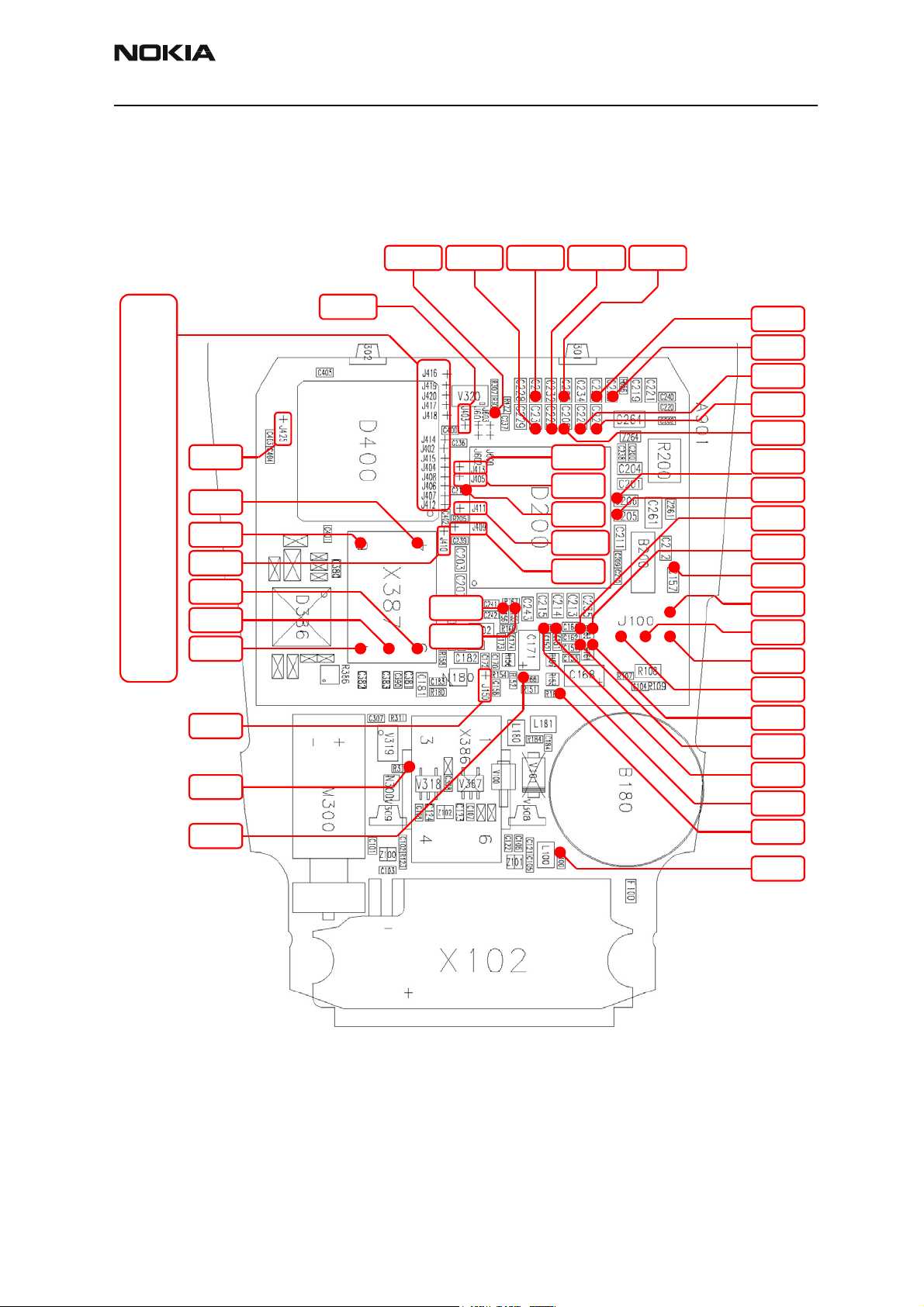
Baseband Troubleshooting
Baseband Testpoints
Baseband testpoint PWB Placement
R306
DLIGHT
C230
VREFRF02
C231
VREFRF01
C222
VR4
C225
VR6
J416
EXTWRX
-
J419
FLSCLK
-
J420
FLSCSX
-
J417
EXTRDX
-
J418
FLS2CSX
-
J414
DBUSDA
-
J402
PURX
-
J413
DBUSEN1X
-
J404
SLEEPCLK
-
J408
CBUSENX
-
J406
CBUSCLK
-
J407
CBUSDA
-
J412
FBUSRX
J425
RFCLK
4
GND
6
SIM I/O
J410
MBUSRX
3
VSIM
2
RST
1
CLK
J150
HOOKINT
R310
KLIGHT
R166
MICB2
J403
SLEEPX
C156
MIC2P
C155
MIC2N
J413
DBUSCLK
J405
UEMINT
C218
VIO
J411
FBUSTX
J409
MBUSTX
C226
VR5
C223
VR2
C227
VR3
C224
VR7
C208
VCORE
C206
VANA
C205
VFLASH1
R183/1
HFCM
R183/2
HF
C157
HEADINT
PRODTP6
VPP
PRODTP7
MBUS
PRODTP2
FBUS TX
PRODTP3
FBUS RX
R161/1
EARP
R161/2
EARN
R164
MIC1N
R164
MIC1P
R165
MICB1
C100
VCHARIN
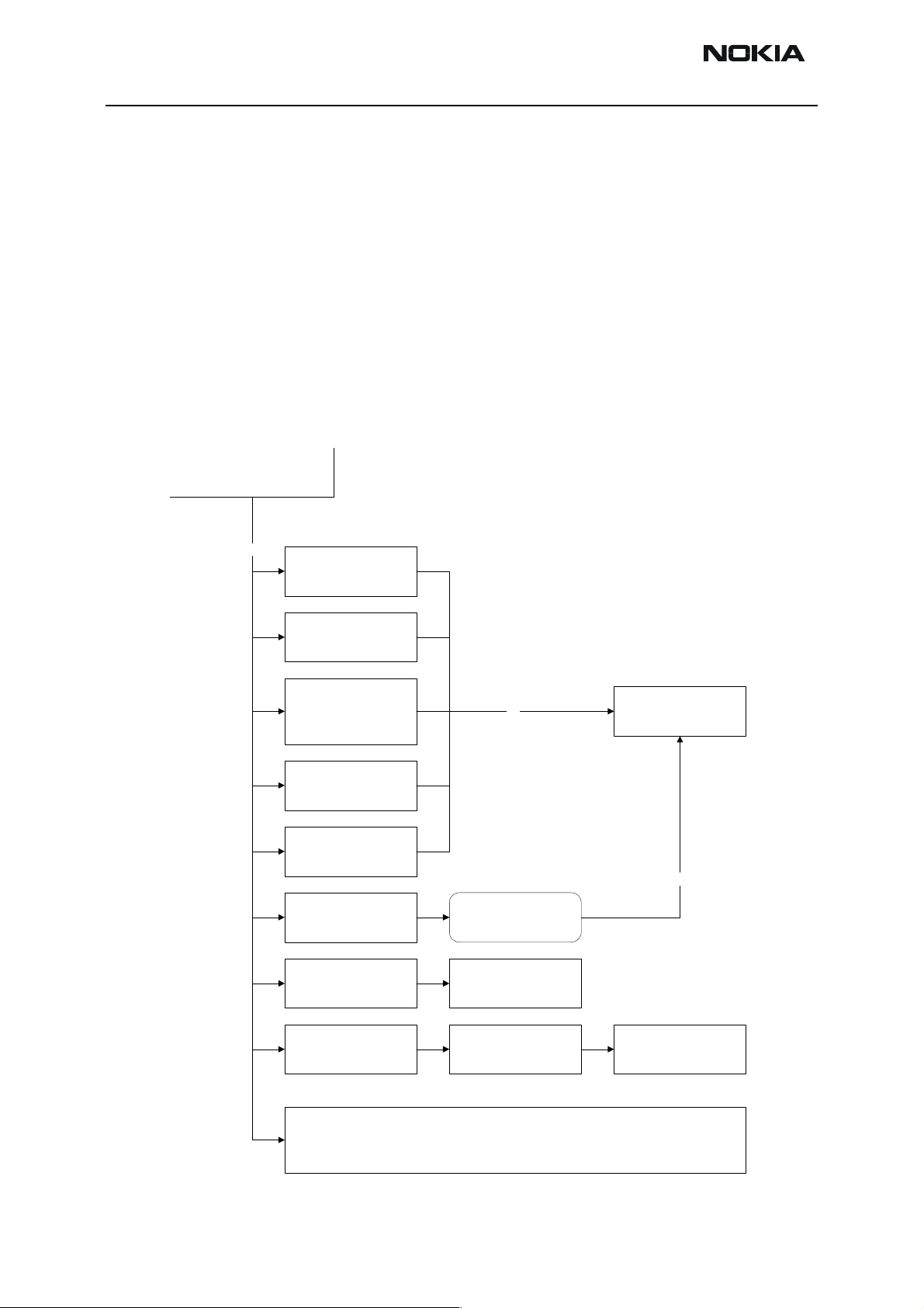
Fault Finding Charts
In this section, fault finding charts are provided for the most common NHM-8NX errors.
NOTE : Since both D200 (UEM) and D400(UPP) is underfilled, they can not be
replaced. If either D200 or D400 is defective, the whole PWB has to be dis-
Issue 1 05/02 ãNokia Corporation Page 5
Page 6

NHM-8NX
Troubleshooting Instructions PAMS Technical Documentation
carded.
Page 6 ãNokia Corporation Issue 1 05/02
Page 7
NHM-8NX
PAMS Technical Documentation Troubleshooting Instructions
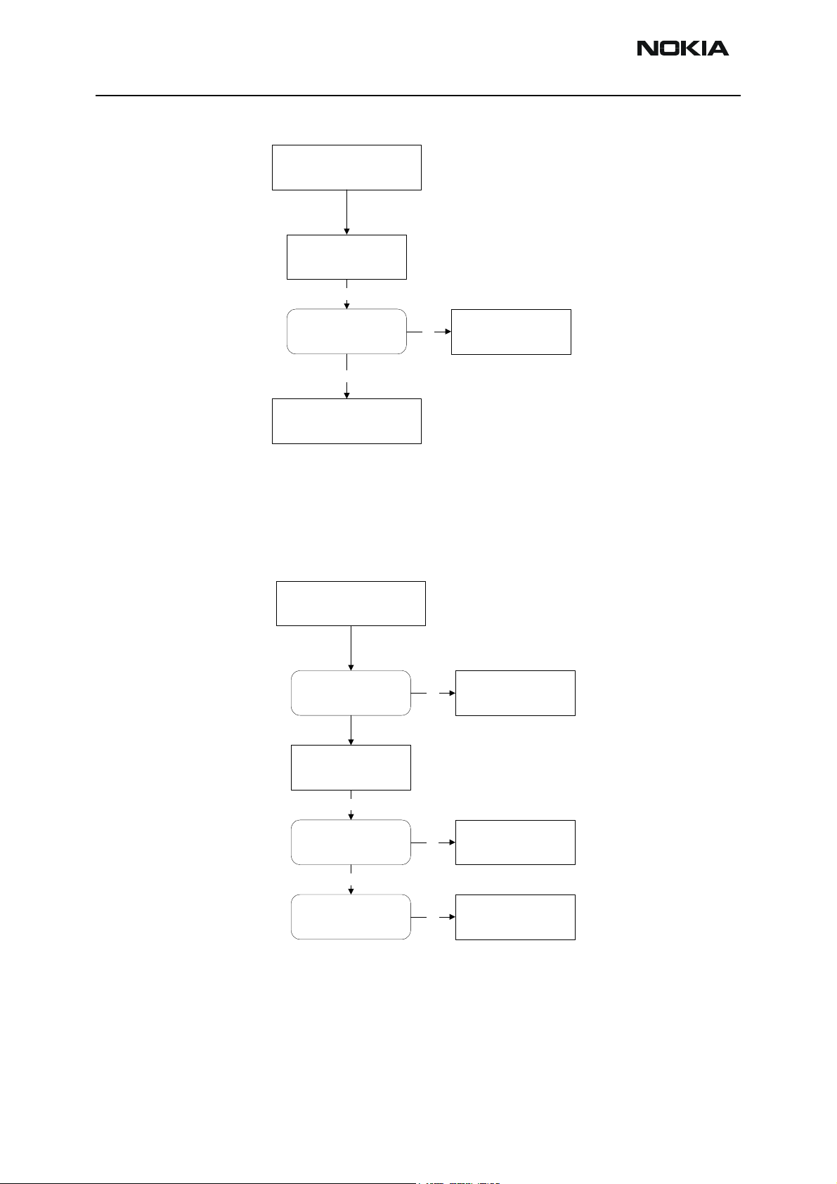
Phone is dead
This means that the phone do not draw any current at all when supply is connected and/
or powerkey is pressed.
It is assumed that the voltage supplied is 3.6 VDC. The UEM will prevent any functionality what so ever at battery/supply levels below 2.9 VDC
Phone is dead
Yes
X101
VBAT = 3,6VDC
Yes
Z261, C261, Z264,
C264
Voltage = 3,6VDC
Yes
S300
Pin 1 & 3 is HIGH when
power-key is untouched
Yes
S300
Pin 1 & 3 is 0VDC(LOW)
when power-key is pressed
Yes
J404
Sleep-clock is
32.768 kHz, 1,8Vpp
Yes
J402
PURX = 1,8VDC,
1 sec. after power-key
is pressed
Yes
No
No
Z261, C261, Z264, C264
No
No
No
B200, C209, C210, PWB.
No
Check :
X101
Check :
Check :
R317, C310
Check :
S300, PWB
Check :
Else defective D200*
Check :
PWB.
Else defective D200*
C227
VR3 = 2,78VDC
Yes
J425
26 MHz clock min.
300mVACpp,
probe Cin=10-13 pF/10M
Yes
Check :
D450 (Flash).
Else defective D200*
No
No
Check :
C227, PWB.
Else defective D200*
Check :
C227, PWB.
Else defective D200*
Issue 1 05/02 ãNokia Corporation Page 7
Page 8
NHM-8NX
Troubleshooting Instructions PAMS Technical Documentation
Flash programming does not work
The flash programming can only be done via the pads on the PWB (J100).
In case of Flash failure in FLALI station, problem is most likely related to SMD problems.
Possible failures could be short-circuit of balls under µBGAs (UEM, UPP, FLASH). Missing
or misaligned components.
In flash programming error cases the flash prommer can give some information about a
fault.
The fault information messages could be:
- Phone doesn't set FBUS_TX line low
Because of the use of uBGA components it is not possible to verify if there is a short circuit in control- and address lines of MCU (UPP) and memory (flash).
Flash prgramming
do not work
Error from prommer:
"Phone doesn't set
FBUS_TX line low"
Yes
J100, R108
Check connection between
pad 1,2 & 3 on J100
and R108
Yes
J409, J410, J411, J412
Voltage level at 1,8VDC
Yes
Try reading MCU ID
with Phoenix.
Reading OK?
Yes
Try reading Flash ID
with Phoenix.
Reading OK?
No
No
No
No
Check :
R108, PWB
Check :
PWB.
Else defective D200*
Check :
PWB.
Else defictive D400*
Check :
Replace D450
Yes
Reflash phone
Page 8 ãNokia Corporation Issue 1 05/02
Page 9
NHM-8NX
PAMS Technical Documentation Troubleshooting Instructions
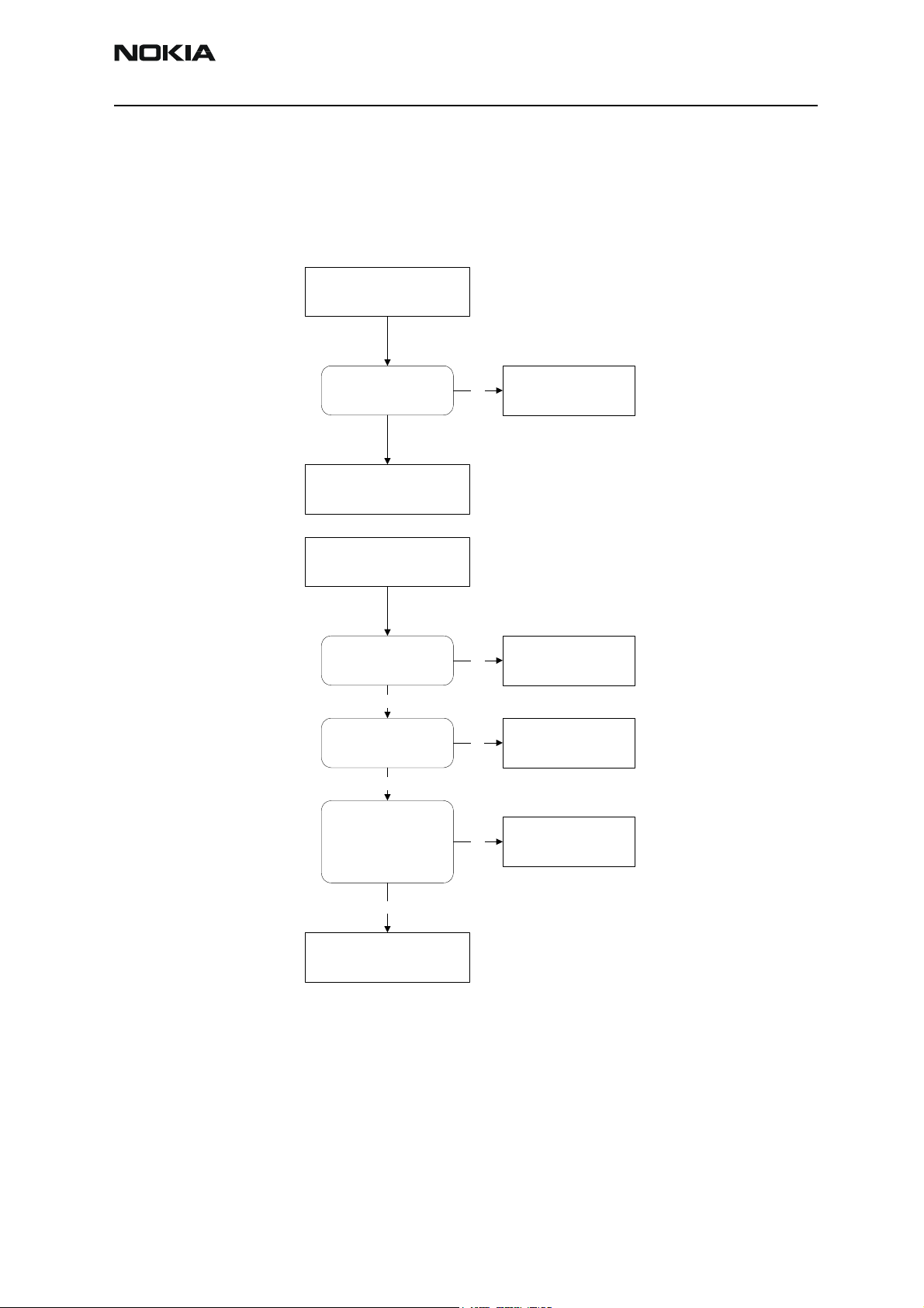
Power does not stay on or phone is jammed
If this kind of failure is presenting itself immediately after FLALI, it is most likely caused
by ASICs missing contact with PWB.
If for some reason the MCU does not service the watchdog register within the UEM, the
operations watchdog will run out after approximately 32 seconds. Unfortunately, the
service routine can not be measured.
Power doesn't stay on,
or phone is jammed
J404
Sleep clock = 32.768 kHz,
1.8Vpp
Yes
J402
PURX = 1,8VDC,
1 sec. after power-key is
pressed
Yes
UI functionality,
and keys react
to pressure?
Yes
J425
26 MHz clock min.
300mVACpp,
probe Cin=10-13 pF/10M
Yes
Reflash phone
No
B200, C209, C210, PWB.
No
No
No
Check :
Else defective D200*
Check :
PWB.
Else defictive D200*
Check :
D450, Keymat,
Lightguide, PWB.
Else defective D400*
Check :
C425, C426, R425,
R426, N600(Mjoelner)
Issue 1 05/02 ãNokia Corporation Page 9
Page 10
NHM-8NX
Troubleshooting Instructions PAMS Technical Documentation
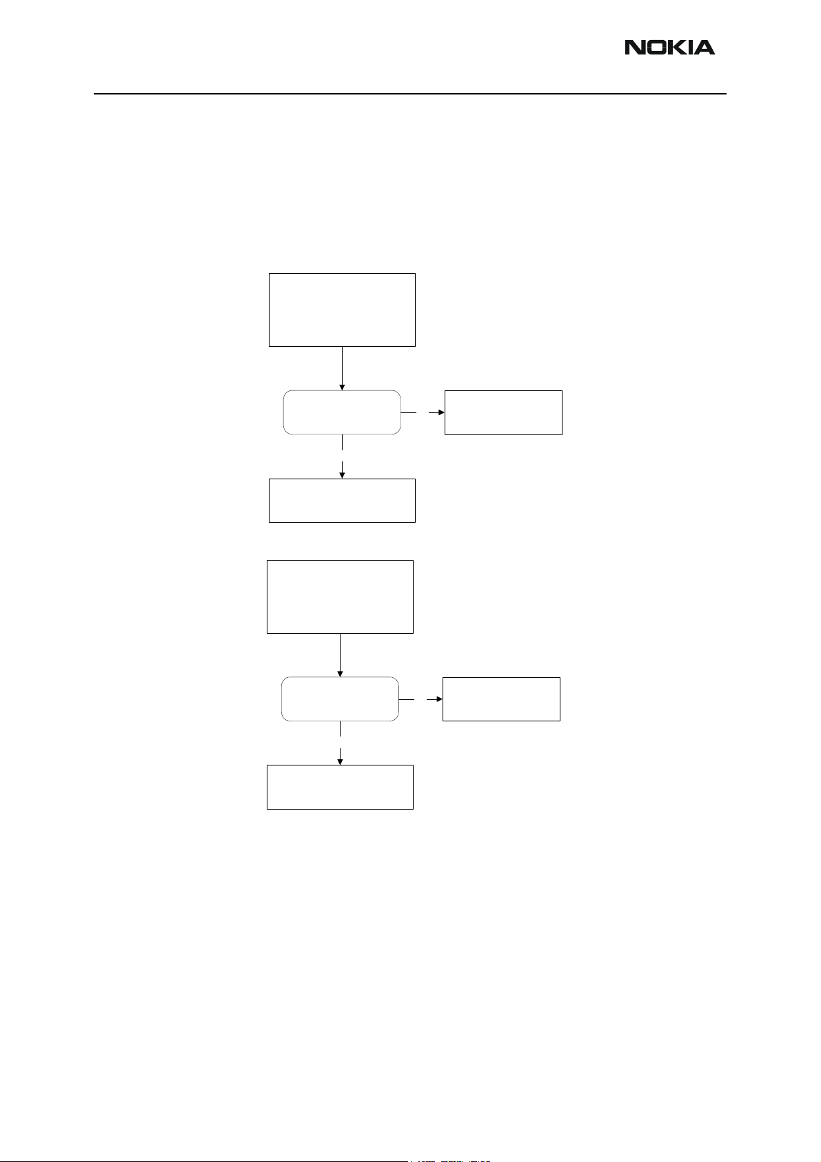
Display information: "Contact Service"
This error can only happen at power up where several self-tests is run. If any of these test
cases fails the display will show the message: "Contact Service".
It's individual test cases so the below lineup of error hunting's has no chronological
order. Use common sense and experience to decide which test case to start error hunting
at.
Display shows
"Contact Service"
Yes
AuxDa & UEMInt
SleepX & SleepClk
between UPP & UEM?
TXI/QD & RXI/QD?
SIM interface between
EarDa & MicDa
between
UPP and UEM?
MBUS interface
between
UPP and UEM?
between
UPP and UEM?
UPP & UEM
Key is stucked
No
R205
Check R205
(no short/open-circuit)
Check :
A-cover, Keymat, Lightguide,
PWB.
Check :
PWB.
Else defective D200*
or D400*
Error still present
Flash checksum
ASIC version vs. compilation flag, PMM checksum
PMM validity
Warrenty Information State
SIM-Lock
Reflash phone
Check :
Else defective D450 (FLASH)
PWB.
Page 10 ãNokia Corporation Issue 1 05/02
Page 11
NHM-8NX
PAMS Technical Documentation Troubleshooting Instructions
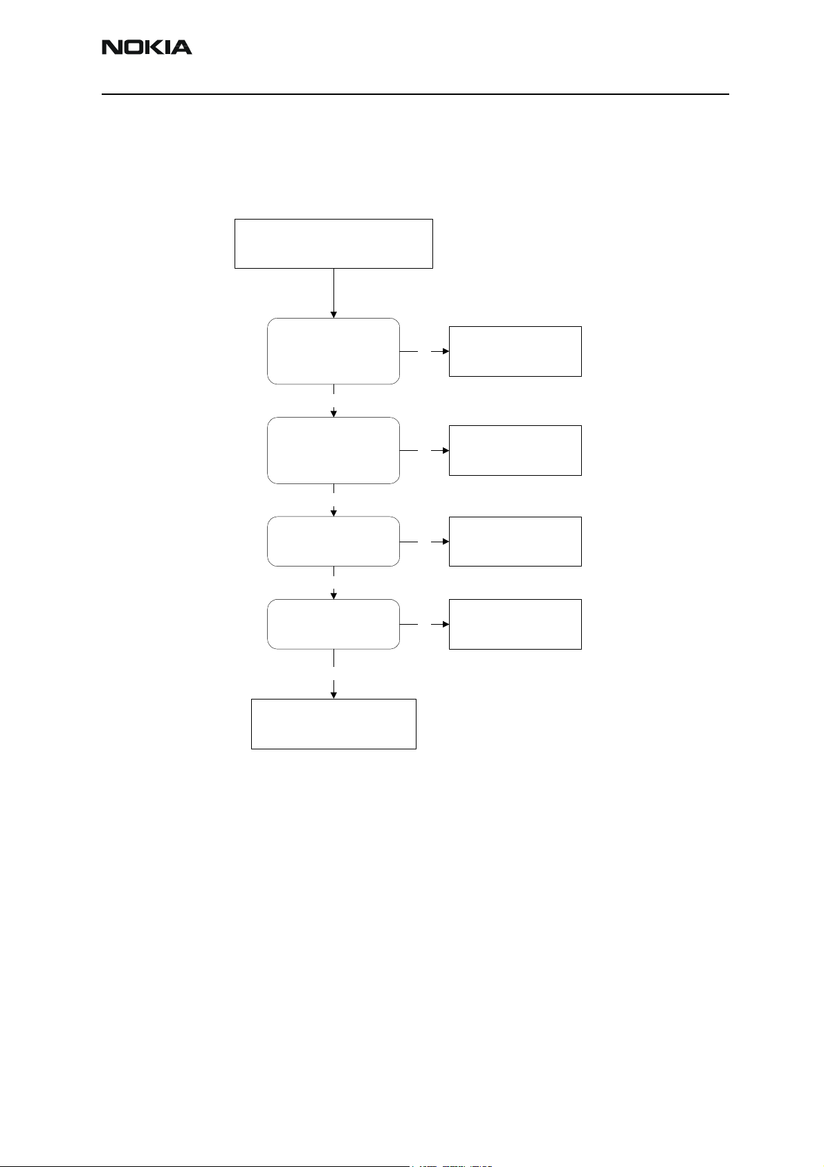
Phone does not register onto the network, or the phone cannot make a call
If the phone doesn't register to the network, the fault can be in either BB or RF. Only few
signals can be tested since several signals is 'burried' in one or more of the inner layers of
the PWB.
First of all check that SIM LOCK is not causing the error by using a Test-SIM card and
connect the phone to a tester.
Phone do not register to
or phone cannot make a call
network
C222, C233, C224, C225,
C226, C227
Voltage = ~2,78VDC
All during GSM frame-
call mode.
Use TXP on C646 as trigger
Yes
C230, C231
Voltage = ~1,35VDC
All during GSM frame (call mode)
Use TXP on C646 as trigger
Yes
J608, J609, J610
Check RF serial bus during
GSM-frame :
Logic HIGH = 1,8VDC
Logic LOW = 0VDC
RFBUSCLK (J608),
RFBUSDA (J609),
RFBUSEN1X (J610)
Yes
R601, R603
Check analog signals during
GSM-frame (RX slot):
RXIP/N (R601) = 0-1,45VDC
RXQP/N (R603) = 0-1,45VDC
Yes
R610, R611
Check analog signals during
GSM-frame (TX slot):
TXIP/N (R610) = 1-1,75VDC
TXQP/N (R611) = 1-1,75VDC
C222,C223, C224, C225,
No
No
No
No
No
C226, C227, PWB.
Else defective D200 or D400*
C230, C231, PWB.
Else defective
D200* or D400*
Else defective D200*
Else defective D200*
R610, R611,PWB.
Else defective D200*
Check :
Check :
Check :
PWB.
or D400*
Check :
PWB.
or D400*
Check :
or D400*
Yes
Check RF
Issue 1 05/02 ãNokia Corporation Page 11
Page 12
NHM-8NX
Troubleshooting Instructions PAMS Technical Documentation
SIM related faults
Insert SIM card fault
The hardware of the SIM interface from UEM (D200) to the SIM connector (X387) can be
tested without a SIM card. When the power is switched on the phone first check for a
1,8V SIM card and then a 3V SIM card. The phone will try this four times, whereafter it
will display ”Insert SIM card”.
Display shows :
"Insert SIM Card"
Yes
Check for SIM voltage during power-up
Ch1 : VSIM
Ch2 : RESET
X387
Verify that phone checks for
1,8V-SIM, and then 3V-SIM
during power-up.
(See illustration below)
Yes
SIM Interface OK
No
Check :
X387, R386, PWB.
Else defective D200*
Ch3 : CLOCK
Ch4 : DATA
Page 12 ãNokia Corporation Issue 1 05/02
Page 13
NHM-8NX
PAMS Technical Documentation Troubleshooting Instructions
SIM-Card rejected
The error ”SIM card rejected” means that the ATR message received from SIM card is corrupted, e.g. data signal levels are wrong. The first data is always ATR and it is sent from
card to phone.
Display shows :
"SIM Card Rejected"
Yes
VSIM = min. 1,6V(1,8V Card)
X387
VSIM = min. 2,8V(3V Card)
(See illustration below)
Yes
X387
ATR data can be seen at
SIM data pin.
Yes
SIM Interface OK
No
No
Check :
R386, PWB.
Else defective D200*
Check :
X387, R386, PWB.
For reference a picture with normal SIM power-up is shown below.
Normal SIM power-up sequence
Ch1 : VSIM
Ch2 : RESET
Ch3 : CLOCK
Ch4 : DATA
Issue 1 05/02 ãNokia Corporation Page 13
Page 14
NHM-8NX
Troubleshooting Instructions PAMS Technical Documentation
Audio related faults
Earpiece do not work
Replace :
Earpiece
Error still present
Z150, R161
Check Z150, R161 is
working correctly
(no short/open-circuit)
Yes
Defective D200*
No
Check :
R386, PWB.
Else defective D200*
Microphone do not work and
the isn't any mechanical
problem
C103, Z100
Check C103, Z100 is
working correctly
(no short/open-circuit)
Replace :
System Connoctor
Error still present
R165
Check voltage level on
R165 towards UEM (bias)
= 2,1V
Yes
R153
Check voltage level on
R153 towards mic-lines (bias)
= 1,0V - 1,4V
No
No
No
R153, R157,C151, C152,
Replace :
C103 and/or Z100
Check :
R165, C168, PWB.
Else defctive D200*
Check :
C153, C154, PWB.
Page 14 ãNokia Corporation Issue 1 05/02
Page 15
NHM-8NX
PAMS Technical Documentation Troubleshooting Instructions
Headset earpiece do not
work and the isn't any
mechanical problem
R183, Z102
Check R183, Z102 is
working correctly
(no open-circuit)
Defective D200*
Headset microphone do not
work and the isn't any
mechanical problem
R166
Check voltage level on R166
towards UEM (bias) = 2,1V
Yes
R151
Check voltage level on R151
towards UEM (bias)
= 1,0V - 1,4V
Yes
R152, R165, R168,
C155, C156, C172,
C170, C173, C174,
Z101
Check XMIC line to UEM
(D200)
No
No
No
No
Replace :
C183 and/or Z102
Replace :
C183 and/or Z102
Check :
R166, R151, C171
Replace :
Defective component
Error still present
Defective D200*
Issue 1 05/02 ãNokia Corporation Page 15
Page 16
NHM-8NX
Troubleshooting Instructions PAMS Technical Documentation
Charging failure
Phone is OFF - battery is
completely empty
(<=3,1VDC)
and no current from
charger when connected
L100
VCHAR > 2,1VDC
Yes
Defective D200*
Phone is ON or OFF - battery
nominal voltage (~3,6VDC)
and no current from
charger when connected
L100
VCHAR > 3,6VDC
Yes
Defective
D200 or D400*
No
F100, L100, V101, C100,
R200, System-connector.
No
F100, L100, V101, C100,
R200, System-connector.
Check :
Check :
Page 16 ãNokia Corporation Issue 1 05/02
Page 17
NHM-8NX
PAMS Technical Documentation Troubleshooting Instructions
Display info when
charger is connected :
"Not charging"
R206
Voltage on R206 towards
D200 is ~0,8VDC
when power is connected.
(BSI must be 75K)
Yes
No
Check :
X101, R202, R206, C240.
Voltage (use scope) on R207
R207
towards D200 is ~0,9VDC at
peak.
(BTEMP must be 47K)
Yes
R200
Voltage on R200 towards
D200 same as VBAT voltage
Yes
R200
Voltage rises slowly on
R200 towards D200 when
charger is connected.
Yes
Check :
PWB
No
No
No
Check :
X101, R202, R207, C220.
Check :
R200, PWB.
Else defective D200*
Check :
PWB.
Else defective D200*
Issue 1 05/02 ãNokia Corporation Page 17
Page 18

NHM-8NX
Troubleshooting Instructions PAMS Technical Documentation
RF Troubleshooting
Two types of measurements are used in the following. It will be specified if the measurement type is "RF" or "LF".
• RF measurements should be done with a Spectrum Analyser and a high-frequency 500 ohm passive probe, for example HP54006A. (Note that when measuring with the 500 ohm probe the signal will be around 20 dB attenuated. The
values in the following will have these 20 dB subtracted and represent the real
value seen on the spectrum analyser).
Note that the testjig have some losses which must be taken into consideration when
calibrating the test system.
• LF (Low frequency) and DC measurements should be done with a 10:1 probe and
an oscilloscope. The probe used in the following is 10MW/8pF passive probe. If
using another probe then bear in mind that the voltages displayed may be
slightly different.
Always make sure the measurement set-up is calibrated when measuring RF parameters
on the antenna pad. Remember to include the loss in the module repair jig when
realigning the phone.
Most RF semiconductors are static discharge sensitive. So ESD protection must be
taken during repair (ground straps and ESD soldering irons). Mjoelner and Bifrost is moisture sensitive so parts must be pre-baked prior to soldering.
Apart from key-components described in this document there are a lot of discrete components (resistors, inductors and capacitors) for which troubleshooting is done by checking if soldering of the component is done properly and checking if the component is
missing from PWB. Capacitors can be checked for short-circuiting and resistors for value
by means of an ohmmeter, but be aware in-circuit measurements should be evaluated
carefully.
In the following both the name EGSM and GSM900 will be used for the lower band and
both PCN and GSM1800 will be used for the upper band.
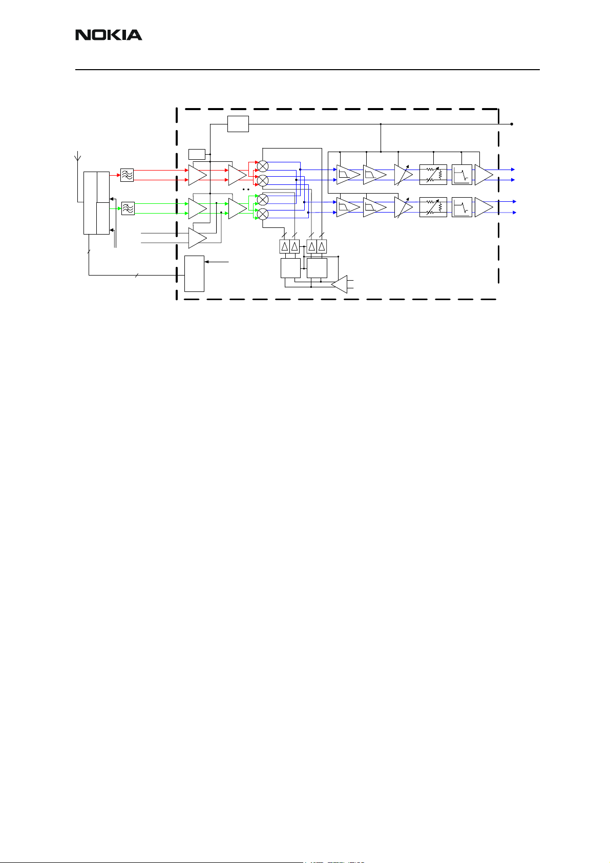
General description of the RF circuits
In the following general descriptions different colours are used in the block diagram. The
GSM 900 signal route is shown in red, the GSM1800 route in green and the common signal lines are shown in blue. Signal lines which is common for both
Receiver signal path
The signal from the antenna pad is routed to the RX/TX switch ( Z700). If no control voltage is present at VANT2 and VANT1 the switch works as a diplexer and the GSM900 signal is passed through the RX/TX switch to GSM-RX and the GSM1800 signal is passed to
DCS-RX.
Page 18 ãNokia Corporation Issue 1 05/02
Page 19
NHM-8NX
PAMS Technical Documentation Troubleshooting Instructions
Figure 1: Receiver signal path
RX
Supply
filter
F
X
R
D
D
V
LNA
RX/TX
Z700
Ant
2
SAW
Z602
SAW
Z601
RX900
RX1800
RX1900
2
VANTL / VANTM
RX
GSM
TX
RX
Switch
PCN
TX
INPL
INML
INPM
INMM
INPH
INMH
Bias
LNA
LNA
LNA
RF
Controls
VDDDIG
Pregain
Pregain
22 22
1/2 1/4
BBAMP
BBAMP
LPF1
LPF1
B
B
X
R
D
D
V
DCN1
DCN1
Mjoelner
N600
BIQUAD
AGC
LPF2
BIQUAD
AGC
LPF2
From the RX/TX switch the GSM900 signal is routed to the SAW filter (Z602). The purpose of the SAW filter is to provide out-of band blocking immunity and to provide the
LNA in Mjoelner (N600) with a balanced signal. The front end of Mjoelner is divided into
a LNA and Pre-Gain amplifier before the mixers.
DCN2
DCN2
VRX
VR6
RXIP
RXIM
RXQP
RXQM
The output from the mixer is feed to Baseband part of Mjoelner where the signals amplified in the BBAMP and low pass filtered in LPF1 before the DC compensation circuits in
DCN1. The DCN1 output is followed by a controlled attenuator and a second lowpass filter LPF2. The output from LPF2 is DC centered in DCN2 before being feed to the BB for
demodulation.
The GSM1800 signal chain is similar to GSM900, the SAW filter numbered Z601.
Transmitter signal path
The I/Q signal from the BB is routed two the modulators for both 900 and 1800 MHz. The
output of the modulators is either terminated in a SAW filter ( Z603 ) for GSM 900 or a
balun for GSM1800. Both signals are amplified in buffers whereby a limiting effect takes
place to suppress some of the AM contents of the signal. The amplitude limited signal is
then amplified in the PA (N700) where the gain control takes place. In order to control
the TX level a sample of the signal is taken in a directional coupler ( L709 for GSM900
and L704 for GSM1800) and used in the power loop amplifier in Mjoelner to establish
the right output power. The TX signal from the couplers is feed to the RX/TX switch, used
to select which signal to route to the antenna.
Issue 1 05/02 ãNokia Corporation Page 19
Page 20

NHM-8NX
Troubleshooting Instructions PAMS Technical Documentation
Figure 2: Transmitter signal path
2
Ant
Switch
RX/TX
Z700
RX
GSM
TX
RX
PCN
TX
L704
Dir.
Coupler
L709
DET
VBATTRF
PA
N700
PCN
V701
Buffer
Buffer
EGSM
V702
VANTL / VANTM
2
Balun
VTX
SAW
Z603
PWloop
filter
VPCH/VPCL
VANTH
VB_DET
VTXLOL
VTXLOH
VTXBH
VTXBL
DET
PLFB1
PLFB2
2
Controls
Controls
OUTHP
OUTHM
OUTLP
OUTLM
VDDDIG
RF
VDDRXBB
RF
PWC
TXC
TXP
TX
P
VDDTX
Supply
filter
VTX
TX
VR2
C
Mjoelner
N600
1/2
2
2
2
TXQM
TXQP/
1/4
2
2
2
TXIM
TXIP/
PLL
The PLL supplies Local Oscillator (LO) signals for the RX and TX-mixers. In order to be able
to generate LO-frequencies for the required EGSM and PCN channels a regular synthesiser-circuit is used. All blocks for the PLL except for the VCO, reference X-tal and loopfilter is located in the Mjoelner IC.
The reference frequency is generated by a 26MHz Voltage Controlled X-tal Oscillator
(VCXO) which is located in the Mjoelner IC. Only the X-tal is external. 26MHz is supplied
to BB where a divide-by-2 circuit (located in the UPP IC) generates the BB-clock at
13MHz. The reference frequency is supplied to the reference divider (RDIV) where the
frequency is divided by 65. The output of RDIV (400kHz) is used as reference clock for the
Phase Detector (ϕ).
The PLL is a feedback control system controlling the phase and frequency of the LO-signal. Building blocks for the PLL are: Phase detector, Charge Pump, Voltage Controlled
Oscillator (VCO), N-Divider and loopfilter. As mentioned earlier only the VCO and loopfilter is external to the Mjoelner IC.
The VCO (G600) is the component that actually generates the LO-frequency. Based on
the control voltage input the VCO generates a single-ended RF output. The signal is then
differentiated through a balun. This signal is fed to the Prescaler and N-divider in Mjoelner, these 2 block will together divide the frequency by a ratio based on the selected
channel. The divider output is supplied to the phase detector which compares the frequency and phase to the 400kHz reference clock. Based on this comparison the phase
Page 20 ãNokia Corporation Issue 1 05/02
Page 21

NHM-8NX
PAMS Technical Documentation Troubleshooting Instructions
detector controls the charge pump to either charge or discharge the capacitors in the
loopfilter. By charging/discharging the loopfilter the control voltage to the VCO changes
and the LO-frequency will change. Therefore the PLL will make the LO-frequency stay
locked to the 26MHz VCXO frequency.
The loopfilter consists of the following components: C639-C641 and R618-R619.
The PLL is operating at twice the channel center frequency when transmitting or receiving in the PCN band. For the EGSM band the PLL is operating at 4-times the channel frequency. Therefore divide-by-2 and divide-by-4 circuits are inserted between the PLL
output and LO-inputs to the PCN and EGSM mixers.
Table 1: Frequency plan
Frequency band Channel System Frequency Band (MHz) PLL Frequency band (MHz)
EGSM RX 975-1023
TX 880.2 – 914.8 3520.8 – 3659.2
1 - 12
925.2 - 959.8 3700.8 - 3839.2
PCN RX 512 – 885 1805.2 – 1879.8 3610.4 – 3759.6
TX 1710.2 – 1784.8 3420.4 – 3569.6
According to the table above the PLL must be able to cover the frequency range
3420.4MHz to 3839.2MHz.
Figure 3: Synthesiser
To PC N RX
mixer
2 22
2
1/2 1/4
1/2 1/4
2
222
To PCN
Modulator
Mjoelner
N600
To GSM RX
mixer
To GSM
Modulator
VDDRXBB
Resistor Ext/R2H/R2
VBEXT
Ref.
filter
VREF1
RFCONV_0(9)
Main B ias
Circ uit
VDDLO
VDDPLL
VDDPRE
Buffer
VDDCP
CPOU T
VDDXO
VDDBBB
REFOUT
XTA LM
XTALP
INPLO
INMLO
VDDDIG
VDDDL
SELADDR
RESETX
RF_E N
RF_CLK
RF_DA TA
RESETX
VCOSENSE
Cha rge
Pump
Lock
Det ect
1/2
I/O
level
shift
3
64/
65
RBEXT
LOCNT
REFCN T
2,7k
NDIV
ADIV
VCXO Bias
VDDRXBB
SENSE
Rpa
PA vend or
indication
18k : Hitachi
82k : RFMD
RDI V
R2H/R2
VDDTX
Sensor
BIST / Temp.
ϕ
AGC
AFC/ CAL
Cont rol
Buf/
Digital
Control
3
26MHz
Synth
supply
filter
Vcp
supply
filter
PLL
loop
filter
VCXO
supply
filte r
VCTRL
REFO UT (26M Hz)
VCO (G600)
RESETX_Mjoel
RF Key component placement
VPLL
VXO
VVCO
VBB (1.8V)
Ref clk set
RFBUSX
RFBUSDA
RFBUSCLK
VR1A
VR5
VR3
VR7
VR2
VIO
VIO
GENIO6
Issue 1 05/02 ãNokia Corporation Page 21
Page 22

NHM-8NX
Troubleshooting Instructions PAMS Technical Documentation
Figure 4: Key component location
Table 2:
N600 Mjoelner RF IC
Z601 PCN RX SAW
Z602 EGSM RX SAW
Z603 EGSM TX SAW
B600 26 MHz crystal
G600 VCO ( 3.6 GHz UHF VCO )
N700 Power Amplifier (PA)
Z700 RX/TX switch
Power Supply Configuration
All power supplies for the RF Unit are generated in the UEM IC (D200). All power outputs
from this IC has a decoupling capacitor at which the supply voltage can be checked.
The power supply configuration used in the HDb12 phone is shown in the blockdiagram
below:
Page 22 ãNokia Corporation Issue 1 05/02
Page 23

NHM-8NX
PAMS Technical Documentation Troubleshooting Instructions
Figure 5: Power supply configuration
PA
UEM
Battery
VR2
VR3
VR5
VR1A
VR6
MJOELNER
Vtx
VXO
VPLL
VCP
Vrx
Vbb
VddXO
Vddbbb
VddRXF
VddRXBB
VddTX
Vdddig
VddPLL
VddLO
VddPre
VddCP
VIO
Vref01
VR7
Vvco
Vref1
Vbext
module
Sel_addr
VddDL
VCO
The names in bold are signal names used on the RF schematic pages. Names in the boxes
within the Mjoelner and the VCO refers to pin names on the respective ICs (N600, G600).
Table 3:
Supply name RF Supply name UEM Min Typ Max Unit
VTX VR2 2.64 2.78 2.86 V
VXO VR3 2.64 2.78 2.86 V
VCP VR1A 4.75 V
VPLL VR5 2.64 2.78 2.86 V
VRX VR6 2.64 2.78 2.86 V
VVCO VR7 2.64 2.78 2.86 V
VBB VIO 1.72 1.8 1.88 V
VREF2 VrefRF01 1.334 1.35 1.366 V
VBATT BATTERY 3.1 3.6 5.2 V
Please see the picture below for measuring points at the UEM (D200).
Issue 1 05/02 ãNokia Corporation Page 23
Page 24

NHM-8NX
1
Troubleshooting Instructions PAMS Technical Documentation
Figure 6: Supply points at UEM (D200)
VR2=Vtx (C643)
VR5=Vpll (C226)
VR7=Vvco (C224)
VR3=Vvcxo (C227)
VR6=Vrx (C225)
Vref01=Vref2 (C23
Receiver
Figure 7: Supply point at Mjoelner (N600)
Vio = Vbb
(C621)
General Instructions for GSM900 RX Troubleshooting
Connect the phone to a PC with the module repair jig.
Start Phoenix and establish connection to the phone
Select File. Select Scan for Product Ctrl-R
Select Maintenance, Testing and then RF Controls
Page 24 ãNokia Corporation Issue 1 05/02
Page 25

NHM-8NX
PAMS Technical Documentation Troubleshooting Instructions
Select:
Band: GSM900
Active Unit: RX
Operation Mode: Continuous
Rx/Tx Channel: 37
AGC: 9
The setup should now look like this:
Issue 1 05/02 ãNokia Corporation Page 25
Page 26

NHM-8NX
Troubleshooting Instructions PAMS Technical Documentation
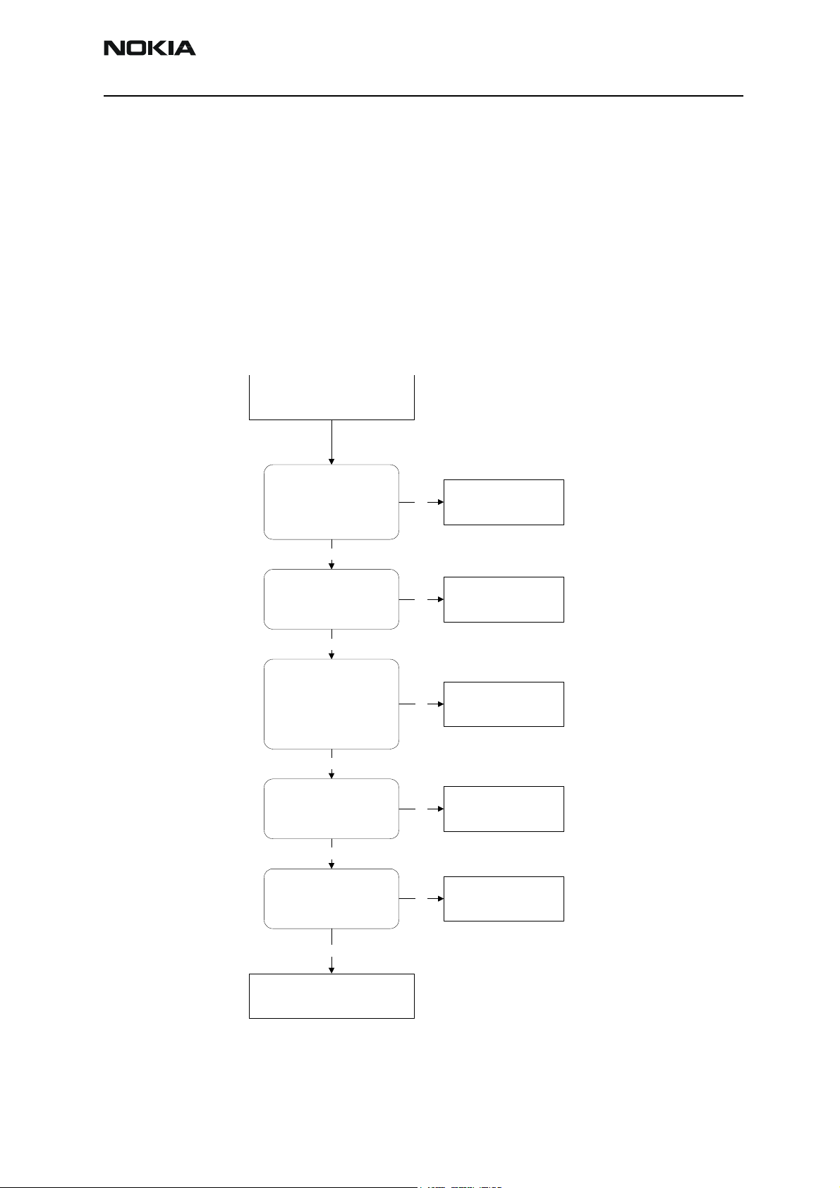
Fault Finding Chart for GSM900 Receiver
Figure 8: EGSM Receiver fault finding chart
1
2
3
4
1
Apply -55 dBm
942.4 MHz, offset
67.71 kHz
from generator to
antenna connector
YES
Oscilloscope at RX
I/Q
signal 588 mVpp
DC offset 1.35 V
freq. 67.71 kHz
YES
EGSM chain
functional
NO
switch at RX 900
Spectrum analyzer
EGSM SAW filter
output -65 dBm
2
Check RX/TX
Z700
-56 dBm
YES
Z602
NO
check Vc1 and Vc2
at Z700 signal 0V
NO
Check SAW filter
3
Oscilloscop
YES
Check RX/TX
switch
Z602
4
NO
Check Mjoelner
YES
YES
Spectrum analyzer
Check signal after
5
inductors L603 and
L602
-65 dBm
NO
Check inductors
L603, L602
YES
Oscilloscope
6
VRX 2.7 V
check Mjoelner
serial interface
NO
Check Base band
By measuring with an oscilloscope at RXIP or RXQP on a working GSM 900 receiver this
picture should be seen.
Signal amplitude peak-peak 588 mV
DC offset 1.33 V
Page 26 ãNokia Corporation Issue 1 05/02
Page 27

NHM-8NX
PAMS Technical Documentation Troubleshooting Instructions
Figure 9: RX900 I/Q signal waveform
General Instructions for GSM1800 RX Troubleshooting
Connect the phone to a PC with the module repair jig.
Start Phoenix and establish connection to the phone
Select File. Select Scan for Product Ctrl-R
Select Maintenance, Testing and RF Controls
Select:
Band: GSM1800
Active Unit: RX
Operation Mode: Continuous
Rx/Tx Channel: 700
AGC: 9
Issue 1 05/02 ãNokia Corporation Page 27
Page 28

NHM-8NX
Troubleshooting Instructions PAMS Technical Documentation
The setup should now look like this:
Page 28 ãNokia Corporation Issue 1 05/02
Page 29
NHM-8NX
PAMS Technical Documentation Troubleshooting Instructions
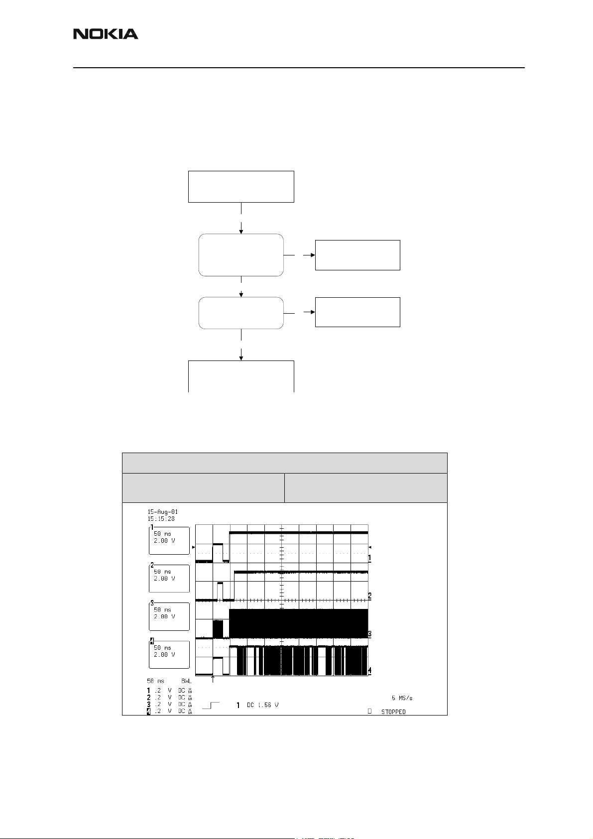
Fault Finding Chart for GSM1800 Receiver
Figure 10: GSM1800 receiver fault finding chart
1
2
3
4
1
Apply -55 dBm
1842.8 MHz, offset
67.71 kHz
from generator to
antenna connector
YES
Oscilloscope at RX
I/Q
signal 408 mVpp
DC offset 1.33 V
freq. 67.71 kHz
YES
PCN chain
functional
NO
switch at RX 1800
Spectrum analyzer
PCN SAW filter
output -65 dBm
2
Check RX/TX
Z700
-57 dBm
YES
Z601
NO
check Vc1 and Vc2
at Z700 signal 0V
NO
Check SAW filter
3
Oscilloscop
YES
Check RX/TX
switch
Z601
4
NO
Check Mjoelner
YES
YES
Spectrum analyzer
Check signal after
5
inductors L611 and
L601
-65 dBm
NO
Check inductors
L611, L601
YES
Oscilloscope
6
VRX 2.7 V
check Mjoelner
serial interface
NO
Check Base band
By measuring with an oscilloscope at RXIP or RXQP on a working GSM 900 receiver this
picture should be seen.
Signal amplitude peak-peak 588 mV
DC offset 1.33 V
Issue 1 05/02 ãNokia Corporation Page 29
Page 30

NHM-8NX
Troubleshooting Instructions PAMS Technical Documentation
Figure 11: RX1800 I/Q signal waveform
Page 30 ãNokia Corporation Issue 1 05/02
Page 31

NHM-8NX
PAMS Technical Documentation Troubleshooting Instructions
Measurement points in the receiver
Figure 12: RX measurements point at the RX/TX Switch - Z700
Vc1
Z700
Vc2
Z700
RX900 output
Z700
Mjoelner input INML
RX900
SAW filter
Z602
SAW filter
RX1800 output
Z700
Figure 13: Measurements points at the RX-Filters – Z601/Z602
RX900
L602
bal output
RX900
unbal input
Z602
RX900
Mjoelner input INPL
L603
RX1800
Mjoelner input INMM
L611
RX900
Mjoelner input INPM
L601
SAW filter
RX1800
SAW filter
unbal input
Z601
RX1800
bal output
Z601
Issue 1 05/02 ãNokia Corporation Page 31
Page 32

NHM-8NX
Troubleshooting Instructions PAMS Technical Documentation
Figure 14: RX I/Q Signals, Baseband shielding can UEM (D200)
RXQM
D200
RXIM
D200
RXIP
D200
RXQP
D200
Transmitter
Measurement points for the transmitter
Figure 15: TX measuremnet points in the PA ( N700 ) shielding can
Vcon1_GSM
ANT
DCS-Tx
DET_Out
GSM-Tx
(C717)
Vcon2_DCS
Pout_DCS
Pin_DCS
VPCTRL_P
VTX_B_P
VPCTRL_G
Pout_GSM
(C717)
Pin_GSM
VTX_B_G
'
Page 32 ãNokia Corporation Issue 1 05/02
Page 33

NHM-8NX
'
X
VTX
PAMS Technical Documentation Troubleshooting Instructions
Figure 16 : TX measurement point in Mjolner (N600) shielding can
TXQI
Bal_Input1
Bal_Input1
Bal_Input2
GSM
Bal_Input2
GSM
OUT_D_T
OUT_G_TX
TXIP
TXIM
General instructions for GSM TX troubleshooting
Apply a RF-cable to the RF-connector to allow the transmitted signal act as normal. RFcable should be connected to measurement equipment or to at least a 10-dB attenuator,
otherwise the PA may be damaged.
Start Phoenix-Service-Software and establish a connection to the phone e.g. FBUS.
Select File and Product: Gemini
Select: Maintenance, Testing and RF Controls
Band: GSM 900
Active Unit: TX
Tx Power Level: 5
Tx Data Type: Random
Issue 1 05/02 ãNokia Corporation Page 33
Page 34

NHM-8NX
Troubleshooting Instructions PAMS Technical Documentation
Your screen should look like:
Measure the output power of the phone; it should be around 32.5 dBm. Remember the
loss in the jig; around 0.3 dB.
Fault finding chart for GSM900 transmitter
Fault finding in output power
For the spectrum analyser measurements in the following chart use the 500 ohm passive
probe. Since the signal measured is bursted it is advised to set the analyser to maxhold.
Page 34 ãNokia Corporation Issue 1 05/02
Page 35

NHM-8NX
PAMS Technical Documentation Troubleshooting Instructions
Figure 16: EGSM900 transmitter fault finding chart
NO
NO
VTX= 2.7 V +
Yes
discretes around
With Scope check :
TXQP
( See figure 19 )
Check TXIP and
Yes
Check Baseband
seriel bus
Checl Mjolner + the
NO
to Z603
-20 dBm
Measure BAL input
input
Measure
OUT_G_TX Buffer
-12 dBm
Measure Pin_GSM
13 dBm
Measure
Pout_GSM
Yes
Yes
-25 dBm
Yes
Yes
Check Z603
( TX SAW filter)
Yes
VTX_B_G = 2.7 V
With Scope check :
VPCTRL_G
( See figure 18 )
With Scope check :
( Coupler )
Check L709
Yes
Check V702
Check N700
+
NO
( PA )
discretes around
NO
NO
TXC
( See figure 18 )
With Scope check :
Yes
Check V700
+
( detector )
discretes around
on GSM-TX.
Power ~ 8 dBm
Measure TX Power
Yes
TX/RX Swith:
Vcon2_DCS = 0V
With Scope check on
Yes
Vcon1_GSM = 2.7 V
Check Z700
( RX/TX Switch )
No No No No No No
> 30.5 dBm
Meter or RCT
ANT with Power
Measure Power on
Yes
Check C739, L702
Issue 1 05/02 ãNokia Corporation Page 35
Page 36

NHM-8NX
o
Troubleshooting Instructions PAMS Technical Documentation
Figure 17: VPCTRL_G & TXC
Yellow trace: Vpctrl_G @ power level 5, ch37
Pink trace: TXC GSM900 band
Fault finding in modulation
The following plots show different situations of TX IQ measurements. Depending on the
time the modulation may cause the signal to look differently.
TX I/Q waveforms
Pink trace: TXQP Blue trace: TXIP - All 1 Pink trace: TXQP Blu etrace: TXIP - Random
Pink trace: TXQP Blue trace: TXIP - All 1 (Zoom In)
Pink trace: TXQP Blu etrace: TXIP - Random ( Zo
Page 36 ãNokia Corporation Issue 1 05/02
Page 37

NHM-8NX
PAMS Technical Documentation Troubleshooting Instructions
I/Q signals look almost the same regardless if modulation is by "1" or by "0". There is no
significante difference between TXIP and TXIM. The same is valid for TXQP and TXQM.
PCN TransmitterGeneral instructions for PCN TX troubleshooting
Apply a RF-cable to the RF-connector to allow the transmitted signal act as normal. RFcable should be connected to measurement equipment or to at least a 10-dB attenuator,
otherwise the PA may be damaged.
Start Phoenix-Service-Software and establish a connection to the phone e.g. FBUS.
Select File. Choose Product: Gemini
Select: Maintenance, Testing and then RF Controls.
Band: GSM 1800
Active Unit: TX
Tx Power Level: 0
Tx Data Type: Random
Your screen should look like:
Measure the output power of the phone; it should be around 28.5 dBm. Remember the
loss in the jig; around 0.7 dB.
Path of the transmitted PCN signal
Fault finding chart for PCN transmitter
Issue 1 05/02 ãNokia Corporation Page 37
Page 38

NHM-8NX
Troubleshooting Instructions PAMS Technical Documentation
Figure 18: GSM1800 transmitter fault finding chart
NO
NO
VTX= 2.7 V +
Yes
discretes around
With Scope check :
to T600
Measure BAL input
Buffer input
Measure OUT_D_TX
-14 dBm
Measure Pin_DCS
Measure
Pout_DCS
Yes
-16 dBm
Yes
-19 dBm
Yes
Yes
11 dBm
Check TXIP an d
With Scope check :
TXQP
Check T600
With Scope check :
VPCTRL_P
Check L709
( See figure 19 )
( PCN Balun)
VTX_B_P = 2.7 V
( See figure 21 )
( Coupler )
Yes
Check Baseband
NO
Yes
Yes
Check V701
+
discretes around
NO
( PA )
Check N700
NO
NO
TXC
( See figure 21 )
With Scope check :
Yes
seriel bus
Checl Mjolner + the
+
( detector )
Check V700
discretes ar ound
Measure TX Power
Measure Power on
on DCS-TX.
Yes
Power ~ 9 dBm
TX/RX Swith:
Vcon2_DCS = 2.7 V
With Scope check on
Yes
Vcon1_GSM = 2.7 V
Check Z700
( RX/TX Switch )
No No No No No No
Yes
> 27.5 dBm
Meter or RCT
ANT with Power
Check C739, L702
Page 38 ãNokia Corporation Issue 1 05/02
Page 39

NHM-8NX
PAMS Technical Documentation Troubleshooting Instructions
Figure 19: VPCTRL_P & TXC
Yellow trace : Vpctrl_P @ power level 0, ch700
Pink trace : TXC PCN1800 band
** TXIQ signals look the same in PCN and GSM
Synthesizer
There is only one PLL synthesizer generating Local Oscillator frequencies for both RX and
TX in both bands ( PCN and EGSM). The VCO frequency is divided by 2 for PCN operation
or by 4 for EGSM operation inside the Mjoelner IC.
General instructions for Synthesizer troubleshooting
Start the Phoenix-Service-Software and
Select: Product: NHM-8NX
Select: Maintenance, Testing and then RF Controls.
Band GSM1800
Active Unit RX
Operation Mode Continuous
RX/TX Channel 700
It is not possible to measure the output of the VCO (G600) directly as this component is
placed underneath a shielding can without detachable lid. However with spectrum analyzer and 500 ohm passive probe it is possible to get an indication if the VCO outputs the
correct frequency. To do this probe R656 – the frequency should be 3685.6MHz and the
power should be around –50 dBm.
26 MHz Reference Oscillator ( VCXO )
The 26 MHz oscillator is located in the Mjoelner IC (N600). The coarse frequency for this
oscillator is set by an external crystal (B600). The reference oscillator is used as a reference frequency for the PLL synthesizer and as the system clock for BaseBand. The
Issue 1 05/02 ãNokia Corporation Page 39
Page 40

NHM-8NX
Troubleshooting Instructions PAMS Technical Documentation
26MHz signal is divided by 2 to achieve 13MHz inside the UPP IC (D400). The 26 MHz
signal from the VCXO can be measured by probing R425 (must be measured on the UPP
side of R425 i.e. the end not connected to C425). The level at this point is approx.
700mVpp. Frequency of this oscillator is adjusted by changing the AFC-register inside the
Mjoelner IC. This is done via the Mjoelner serial interface.
Example Signal Measured at VCXO output (R425)
Figure 20: VCXO 26 MHz waveform
Page 40 ãNokia Corporation Issue 1 05/02
Page 41

NHM-8NX
PAMS Technical Documentation Troubleshooting Instructions
VCO
The VCO is generating frequencies in the range of 3420.2MHz – 3839.2 MHz when the
PLL is running. The output frequency from the VCO is led to the Local oscillator input of
the Mjoelner IC (N600), where the frequency is divided by 2 or 4 so that they can generate all channels in EGSM and PCN respectively. Frequency of the VCO is controlled by a
DC-voltage ( Vctrl ) coming from the loopfilter. The loopfilter consists of the components
R618, R619 and C639-C641. Range of the Vctrl when the PLL is running (locked) is 0.7V
– 3.8V. Even if the PLL is not in locked state (Vctrl out of range) there is some frequency
at the output of the VCO (G600) which is between 3 and 4 GHz. This is of course only
true if the VCO is working and if the VCO power supply is present (2.7V).
Fault finding chart for PLL Synthesizer
Figure 21: PLL fault finding chart
From Phoenix chose:
File
> Choose Product > NHM-8NX
Mainenance
GSM1800 > RX > Continuous > Ch 700
> Testing > RF Controls >
Spectrum Analyzer:
Measure
VCO frequency at R656
3685.6MHz
Yes
PLL block functional
Oscilloscope:
Measure
VCXO Power Supply at C620
2.7 V
Yes
Oscilloscope:
Measure
VCXO output
On (R425) 26 MHz,
Approx. 700mVpp
Yes
Oscilloscope:
Measure
VCO Power Supply
(R656)
2,7 V
Yes
Oscilloscope:
Measure
PLL Power Supply
C614 & C634
Both 2,7 V
Yes
Oscilloscope:
Measure
CP
Supply C616
V
4,7 V
Yes
Spectr um Analyzer:
Measure
VCO output (R656)
Some signal between
3 and 4 GHz
Yes
Oscilloscope:
Measure
Control Voltage C641
between 0.5 and 4.0 V
Yes
Check
Mjoeln er N600,
UPP D400,
RFBusClk J608,
RFBusDA J610,
RFBusX j609
& Reset_Mjoel
No
No
No
No
No
No
No
UEM, Software??
Phone not in function
VCXO is not functional
Phone not in function
UEM, Software??
Phone not in function
UEM, Software??
Phone not in function
R603, UEM, Software??
VCO G600 is not functional
Loopfilter R618,R619,
Check
Check
Crystal B600
Check
Check
Check
Check
C639-C641
Issue 1 05/02 ãNokia Corporation Page 41
Page 42

NHM-8NX
Troubleshooting Instructions PAMS Technical Documentation
If the phone stops working a short time after the power is turned ON, a possible reason
forthis might be that the 26MHz system clock signal is not getting to the UPP clockinput in BaseBand. In this case check the following:
1 Turn on the phone and check
2 VCXO Power supply (C620) = 2.7V
3 VCXO output (R425 – end not connected to C425) is 26MHz and approx.
700mVpp
If this is not the case check the reference crystal (B600) and Mjolner (N600) as well as
R425, R426, C425, C426.
Measurement points for the PLL
Measurement points at the VCXO
Figure 22: Measurement point for VCXO supply
VCXO Vcc (C620)
Page 42 ãNokia Corporation Issue 1 05/02
Page 43

NHM-8NX
PAMS Technical Documentation Troubleshooting Instructions
Figure 23: Measurement point for VCXO output
VCXO Output (R425)
Measure at this end!
Measurement points at the PLL/VCO
Figure 24: Measurement point for PLL
VCO Vcc (R656)
VCO Output is also
detected here!
Issue 1 05/02 ãNokia Corporation Page 43
Page 44

NHM-8NX
A
Troubleshooting Instructions PAMS Technical Documentation
CP Vcp (C616)
Vcp=VR1
PLL Vcc
(C614, C634)
Page 44 ãNokia Corporation Issue 1 05/02
Page 45

NHM-8NX
q
PAMS Technical Documentation Troubleshooting Instructions
Frequency lists
GSM900
uency list NHM-5 GSM900
CH TX RX VCO TX VCO RX CH TX RX VCO TX VCO RX CH TX RX VCO TX VCO RX
975 880.2 925.2 3520.8 3700.8 1 890.2 935.2 3560.8 3740.8 63 902.6 947.6 3610.4 3790.4
976 880.4 925.4 3521.6 3701.6 2 890.4 935.4 3561.6 3741.6 64 902.8 947.8 3611.2 3791.2
977 880.6 925.6 3522.4 3702.4 3 890.6 935.6 3562.4 3742.4 65 903 948 3612 3792
978 880.8 925.8 3523.2 3703.2 4 890.8 935.8 3563.2 3743.2 66 903.2 948.2 3612.8 3792.8
979 881 926 3524 3704 5 891 936 3564 3744 67 903.4 948.4 3613.6 3793.6
980 881.2 926.2 3524.8 3704.8 6 891.2 936.2 3564.8 3744.8 68 903.6 948.6 3614.4 3794.4
981 881.4 926.4 3525.6 3705.6 7 891.4 936.4 3565.6 3745.6 69 903.8 948.8 3615.2 3795.2
982 881.6 926.6 3526.4 3706.4 8 891.6 936.6 3566.4 3746.4 70 904 949 3616 3796
983 881.8 926.8 3527.2 3707.2 9 891.8 936.8 3567.2 3747.2 71 904.2 949.2 3616.8 3796.8
984 882 927 3528 3708 10 892 937 3568 3748 72 904.4 949.4 3617.6 3797.6
985 882.2 927.2 3528.8 3708.8 11 892.2 937.2 3568.8 3748.8 73 904.6 949.6 3618.4 3798.4
986 882.4 927.4 3529.6 3709.6 12 892.4 937.4 3569.6 3749.6 74 904.8 949.8 3619.2 3799.2
987 882.6 927.6 3530.4 3710.4 13 892.6 937.6 3570.4 3750.4 75 905 950 3620 3800
988 882.8 927.8 3531.2 3711.2 14 892.8 937.8 3571.2 3751.2 76 905.2 950.2 3620.8 3800.8
989 883 928 3532 3712 15 893 938 3572 3752 77 905.4 950.4 3621.6 3801.6
990 883.2 928.2 3532.8 3712.8 16 893.2 938.2 3572.8 3752.8 78 905.6 950.6 3622.4 3802.4
991 883.4 928.4 3533.6 3713.6 17 893.4 938.4 3573.6 3753.6 79 905.8 950.8 3623.2 3803.2
992 883.6 928.6 3534.4 3714.4 18 893.6 938.6 3574.4 3754.4 80 906 951 3624 3804
993 883.8 928.8 3535.2 3715.2 19 893.8 938.8 3575.2 3755.2 81 906.2 951.2 3624.8 3804.8
994 884 929 3536 3716 20 894 939 3576 3756 82 906.4 951.4 3625.6 3805.6
995 884.2 929.2 3536.8 3716.8 21 894.2 939.2 3576.8 3756.8 83 906.6 951.6 3626.4 3806.4
996 884.4 929.4 3537.6 3717.6 22 894.4 939.4 3577.6 3757.6 84 906.8 951.8 3627.2 3807.2
997 884.6 929.6 3538.4 3718.4 23 894.6 939.6 3578.4 3758.4 85 907 952 3628 3808
998 884.8 929.8 3539.2 3719.2 24 894.8 939.8 3579.2 3759.2 86 907.2 952.2 3628.8 3808.8
999 885 930 3540 3720 25 895 940 3580 3760 87 907.4 952.4 3629.6 3809.6
1000 885.2 930.2 3540.8 3720.8 26 895.2 940.2 3580.8 3760.8 88 907.6 952.6 3630.4 3810.4
1001 885.4 930.4 3541.6 3721.6 27 895.4 940.4 3581.6 3761.6 89 907.8 952.8 3631.2 3811.2
1002 885.6 930.6 3542.4 3722.4 28 895.6 940.6 3582.4 3762.4 90 908 953 3632 3812
1003 885.8 930.8 3543.2 3723.2 29 895.8 940.8 3583.2 3763.2 91 908.2 953.2 3632.8 3812.8
1004 886 931 3544 3724 30 896 941 3584 3764 92 908.4 953.4 3633.6 3813.6
1005 886.2 931.2 3544.8 3724.8 31 896.2 941.2 3584.8 3764.8 93 908.6 953.6 3634.4 3814.4
1006 886.4 931.4 3545.6 3725.6 32 896.4 941.4 3585.6 3765.6 94 908.8 953.8 3635.2 3815.2
1007 886.6 931.6 3546.4 3726.4 33 896.6 941.6 3586.4 3766.4 95 909 954 3636 3816
1008 886.8 931.8 3547.2 3727.2 34 896.8 941.8 3587.2 3767.2 96 909.2 954.2 3636.8 3816.8
1009 887 932 3548 3728 35 897 942 3588 3768 97 909.4 954.4 3637.6 3817.6
1010 887.2 932.2 3548.8 3728.8 36 897.2 942.2 3588.8 3768.8 98 909.6 954.6 3638.4 3818.4
1011 887.4 932.4 3549.6 3729.6 37 897.4 942.4 3589.6 3769.6 99 909.8 954.8 3639.2 3819.2
1012 887.6 932.6 3550.4 3730.4 38 897.6 942.6 3590.4 3770.4 100 910 955 3640 3820
1013 887.8 932.8 3551.2 3731.2 39 897.8 942.8 3591.2 3771.2 101 910.2 955.2 3640.8 3820.8
1014 888 933 3552 3732 40 898 943 3592 3772 102 910.4 955.4 3641.6 3821.6
1015 888.2 933.2 3552.8 3732.8 41 898.2 943.2 3592.8 3772.8 103 910.6 955.6 3642.4 3822.4
1016 888.4 933.4 3553.6 3733.6 42 898.4 943.4 3593.6 3773.6 104 910.8 955.8 3643.2 3823.2
1017 888.6 933.6 3554.4 3734.4 43 898.6 943.6 3594.4 3774.4 105 911 956 3644 3824
1018 888.8 933.8 3555.2 3735.2 44 898.8 943.8 3595.2 3775.2 106 911.2 956.2 3644.8 3824.8
1019 889 934 3556 3736 45 899 944 3596 3776 107 911.4 956.4 3645.6 3825.6
1020 889.2 934.2 3556.8 3736.8 46 899.2 944.2 3596.8 3776.8 108 911.6 956.6 3646.4 3826.4
1021 889.4 934.4 3557.6 3737.6 47 899.4 944.4 3597.6 3777.6 109 911.8 956.8 3647.2 3827.2
1022 889.6 934.6 3558.4 3738.4 48 899.6 944.6 3598.4 3778.4 110 912 957 3648 3828
1023 889.8 934.8 3559.2 3739.2 49 899.8 944.8 3599.2 3779.2 111 912.2 957.2 3648.8 3828.8
0 890 935 3560 3740 50 900 945 3600 3780 112 912.4 957.4 3649.6 3829.6
Fre
51 900.2 945.2 3600.8 3780.8 113 912.6 957.6 3650.4 3830.4
52 900.4 945.4 3601.6 3781.6 114 912.8 957.8 3651.2 3831.2
53 900.6 945.6 3602.4 3782.4 115 913 958 3652 3832
54 900.8 945.8 3603.2 3783.2 116 913.2 958.2 3652.8 3832.8
55 901 946 3604 3784 117 913.4 958.4 3653.6 3833.6
56 901.2 946.2 3604.8 3784.8 118 913.6 958.6 3654.4 3834.4
57 901.4 946.4 3605.6 3785.6 119 913.8 958.8 3655.2 3835.2
58 901.6 946.6 3606.4 3786.4 120 914 959 3656 3836
59 901.8 946.8 3607.2 3787.2 121 914.2 959.2 3656.8 3836.8
60 902 947 3608 3788 122 914.4 959.4 3657.6 3837.6
61 902.2 947.2 3608.8 3788.8 123 914.6 959.6 3658.4 3838.4
62 902.4 947.4 3609.6 3789.6 124 914.8 959.8 3659.2 3839.2
Issue 1 05/02 ãNokia Corporation Page 45
Page 46

NHM-8NX
Troubleshooting Instructions PAMS Technical Documentation
PCN
CH TX RX VCO TX VCO RX CH TX RX VCO TX VCO RX CH TX RX VCO TX VCO RX CH TX RX VCO TX VCO RX
512 1710.2 1805.2 3420.4 3610.4 606 1729 1824 3458 3648 700 1747.8 1842.8 3495.6 3685.6 794 1766.6 1861.6 3533.2 3723.2
513 1710.4 1805.4 3420.8 3610.8 607 1729.2 1824.2 3458.4 3648.4 701 1748 1843 3496 3686 795 1766.8 1861.8 3533.6 3723.6
514 1710.6 1805.6 3421.2 3611.2 608 1729.4 1824.4 3458.8 3648.8 702 1748.2 1843.2 3496.4 3686.4 796 1767 1862 3534 3724
515 1710.8 1805.8 3421.6 3611.6 609 1729.6 1824.6 3459.2 3649.2 703 1748.4 1843.4 3496.8 3686.8 797 1767.2 1862.2 3534.4 3724.4
516 1711 1806 3422 3612 610 1729.8 1824.8 3459.6 3649.6 704 1748.6 1843.6 3497.2 3687.2 798 1767.4 1862.4 3534.8 3724.8
517 1711.2 1806.2 3422.4 3612.4 611 1730 1825 3460 3650 705 1748.8 1843.8 3497.6 3687.6 799 1767.6 1862.6 3535.2 3725.2
518 1711.4 1806.4 3422.8 3612.8 612 1730.2 1825.2 3460.4 3650.4 706 1749 1844 3498 3688 800 1767.8 1862.8 3535.6 3725.6
519 1711.6 1806.6 3423.2 3613.2 613 1730.4 1825.4 3460.8 3650.8 707 1749.2 1844.2 3498.4 3688.4 801 1768 1863 3536 3726
520 1711.8 1806.8 3423.6 3613.6 614 1730.6 1825.6 3461.2 3651.2 708 1749.4 1844.4 3498.8 3688.8 802 1768.2 1863.2 3536.4 3726.4
521 1712 1807 3424 3614 615 1730.8 1825.8 3461.6 3651.6 709 1749.6 1844.6 3499.2 3689.2 803 1768.4 1863.4 3536.8 3726.8
522 1712.2 1807.2 3424.4 3614.4 616 1731 1826 3462 3652 710 1749.8 1844.8 3499.6 3689. 6 804 1768.6 1863.6 3537.2 3727.2
523 1712.4 1807.4 3424.8 3614.8 617 1731.2 1826.2 3462.4 3652.4 711 1750 1845 3500 3690 805 1768.8 1863.8 3537.6 3727.6
524 1712.6 1807.6 3425.2 3615.2 618 1731.4 1826.4 3462.8 3652.8 712 1750.2 1845.2 3500.4 3690.4 806 1769 1864 3538 3728
525 1712.8 1807.8 3425.6 3615.6 619 1731.6 1826.6 3463.2 3653.2 713 1750.4 1845.4 3500.8 3690.8 807 1769.2 1864.2 3538.4 3728.4
526 1713 1808 3426 3616 620 1731.8 1826.8 3463.6 3653.6 714 1750.6 1845.6 3501.2 3691.2 808 1769.4 1864.4 3538.8 3728.8
527 1713.2 1808.2 3426.4 3616.4 621 1732 1827 3464 3654 715 1750.8 1845.8 3501.6 3691.6 809 1769.6 1864.6 3539.2 3729.2
528 1713.4 1808.4 3426.8 3616.8 622 1732.2 1827.2 3464.4 3654.4 716 1751 1846 3502 3692 810 1769.8 1864.8 3539.6 3729.6
529 1713.6 1808.6 3427.2 3617.2 623 1732.4 1827.4 3464.8 3654.8 717 1751.2 1846.2 3502.4 3692.4 811 1770 1865 3540 3730
530 1713.8 1808.8 3427.6 3617.6 624 1732.6 1827.6 3465.2 3655.2 718 1751.4 1846.4 3502.8 3692.8 812 1770.2 1865.2 3540.4 3730.4
531 1714 1809 3428 3618 625 1732.8 1827.8 3465.6 3655.6 719 1751.6 1846.6 3503.2 3693.2 813 1770.4 1865.4 3540.8 3730.8
532 1714.2 1809.2 3428.4 3618.4 626 1733 1828 3466 3656 720 1751.8 1846.8 3503.6 3693.6 814 1770.6 1865.6 3541.2 3731.2
533 1714.4 1809.4 3428.8 3618.8 627 1733.2 1828.2 3466.4 3656.4 721 1752 1847 3504 3694 815 1770.8 1865.8 3541.6 3731.6
534 1714.6 1809.6 3429.2 3619.2 628 1733.4 1828.4 3466.8 3656.8 722 1752.2 1847.2 3504.4 3694.4 816 1771 1866 3542 3732
535 1714.8 1809.8 3429.6 3619.6 629 1733.6 1828.6 3467.2 3657.2 723 1752.4 1847.4 3504.8 3694.8 817 1771.2 1866.2 3542.4 3732.4
536 1715 1810 3430 3620 630 1733.8 1828.8 3467.6 3657.6 724 1752.6 1847.6 3505.2 3695.2 818 1771.4 1866.4 3542.8 3732.8
537 1715.2 1810.2 3430.4 3620.4 631 1734 1829 3468 3658 725 1752.8 1847.8 3505.6 3695.6 819 1771.6 1866.6 3543.2 3733.2
538 1715.4 1810.4 3430.8 3620.8 632 1734.2 1829.2 3468.4 3658.4 726 1753 1848 3506 3696 820 1771.8 1866.8 3543.6 3733.6
539 1715.6 1810.6 3431.2 3621.2 633 1734.4 1829.4 3468.8 3658.8 727 1753.2 1848.2 3506.4 3696.4 821 1772 1867 3544 3734
540 1715.8 1810.8 3431.6 3621.6 634 1734.6 1829.6 3469.2 3659.2 728 1753.4 1848.4 3506.8 3696.8 822 1772.2 1867.2 3544.4 3734.4
541 1716 1811 3432 3622 635 1734.8 1829.8 3469.6 3659.6 729 1753.6 1848.6 3507.2 3697. 2 823 1772.4 1867.4 3544.8 3734.8
542 1716.2 1811.2 3432.4 3622.4 636 1735 1830 3470 3660 730 1753.8 1848.8 3507.6 3697.6 824 1772.6 1867.6 3545.2 3735.2
543 1716.4 1811.4 3432.8 3622.8 637 1735.2 1830.2 3470.4 3660.4 731 1754 1849 3508 3698 825 1772.8 1867.8 3545.6 3735.6
544 1716.6 1811.6 3433.2 3623.2 638 1735.4 1830.4 3470.8 3660.8 732 1754.2 1849.2 3508.4 3698.4 826 1773 1868 3546 3736
545 1716.8 1811.8 3433.6 3623.6 639 1735.6 1830.6 3471.2 3661.2 733 1754.4 1849.4 3508.8 3698.8 827 1773.2 1868.2 3546.4 3736.4
546 1717 1812 3434 3624 640 1735.8 1830.8 3471.6 3661.6 734 1754.6 1849.6 3509.2 3699.2 828 1773.4 1868.4 3546.8 3736.8
547 1717.2 1812.2 3434.4 3624.4 641 1736 1831 3472 3662 735 1754.8 1849.8 3509.6 3699.6 829 1773.6 1868.6 3547.2 3737.2
548 1717.4 1812.4 3434.8 3624.8 642 1736.2 1831.2 3472.4 3662.4 736 1755 1850 3510 3700 830 1773.8 1868.8 3547.6 3737.6
549 1717.6 1812.6 3435.2 3625.2 643 1736.4 1831.4 3472.8 3662.8 737 1755.2 1850.2 3510.4 3700.4 831 1774 1869 3548 3738
550 1717.8 1812.8 3435.6 3625.6 644 1736.6 1831.6 3473.2 3663.2 738 1755.4 1850.4 3510.8 3700.8 832 1774.2 1869.2 3548.4 3738.4
551 1718 1813 3436 3626 645 1736.8 1831.8 3473.6 3663.6 739 1755.6 1850.6 3511.2 3701.2 833 1774.4 1869.4 3548.8 3738.8
552 1718.2 1813.2 3436.4 3626.4 646 1737 1832 3474 3664 740 1755.8 1850.8 3511.6 3701.6 834 1774.6 1869.6 3549.2 3739.2
553 1718.4 1813.4 3436.8 3626.8 647 1737.2 1832.2 3474.4 3664.4 741 1756 1851 3512 3702 835 1774.8 1869.8 3549.6 3739.6
554 1718.6 1813.6 3437.2 3627.2 648 1737.4 1832.4 3474.8 3664.8 742 1756.2 1851.2 3512.4 3702.4 836 1775 1870 3550 3740
555 1718.8 1813.8 3437.6 3627.6 649 1737.6 1832.6 3475.2 3665.2 743 1756.4 1851.4 3512.8 3702.8 837 1775.2 1870.2 3550.4 3740.4
556 1719 1814 3438 3628 650 1737.8 1832.8 3475.6 3665.6 744 1756.6 1851.6 3513.2 3703.2 838 1775.4 1870.4 3550.8 3740.8
557 1719.2 1814.2 3438.4 3628.4 651 1738 1833 3476 3666 745 1756.8 1851.8 3513.6 3703.6 839 1775.6 1870.6 3551.2 3741.2
558 1719.4 1814.4 3438.8 3628.8 652 1738.2 1833.2 3476.4 3666.4 746 1757 1852 3514 3704 840 1775.8 1870.8 3551.6 3741.6
559 1719.6 1814.6 3439.2 3629.2 653 1738.4 1833.4 3476.8 3666.8 747 1757.2 1852.2 3514.4 3704. 4 841 1776 1871 3552 3742
560 1719.8 1814.8 3439.6 3629.6 654 1738.6 1833.6 3477.2 3667.2 748 1757.4 1852.4 3514.8 3704. 8 842 1776.2 1871.2 3552.4 3742.4
561 1720 1815 3440 3630 655 1738.8 1833.8 3477.6 3667.6 749 1757.6 1852.6 3515.2 3705.2 843 1776.4 1871.4 3552.8 3742.8
562 1720.2 1815.2 3440.4 3630.4 656 1739 1834 3478 3668 750 1757.8 1852.8 3515.6 3705.6 844 1776.6 1871.6 3553.2 3743.2
563 1720.4 1815.4 3440.8 3630.8 657 1739.2 1834.2 3478.4 3668.4 751 1758 1853 3516 3706 845 1776.8 1871.8 3553.6 3743.6
564 1720.6 1815.6 3441.2 3631.2 658 1739.4 1834.4 3478.8 3668.8 752 1758.2 1853.2 3516.4 3706.4 846 1777 1872 3554 3744
565 1720.8 1815.8 3441.6 3631.6 659 1739.6 1834.6 3479.2 3669.2 753 1758.4 1853.4 3516.8 3706.8 847 1777.2 1872.2 3554.4 3744.4
566 1721 1816 3442 3632 660 1739.8 1834.8 3479.6 3669.6 754 1758.6 1853.6 3517.2 3707.2 848 1777.4 1872.4 3554.8 3744.8
567 1721.2 1816.2 3442.4 3632.4 661 1740 1835 3480 3670 755 1758.8 1853.8 3517.6 3707.6 849 1777.6 1872.6 3555.2 3745.2
568 1721.4 1816.4 3442.8 3632.8 662 1740.2 1835.2 3480.4 3670.4 756 1759 1854 3518 3708 850 1777.8 1872.8 3555.6 3745.6
569 1721.6 1816.6 3443.2 3633.2 663 1740.4 1835.4 3480.8 3670.8 757 1759.2 1854.2 3518.4 3708. 4 851 1778 1873 3556 3746
570 1721.8 1816.8 3443.6 3633.6 664 1740.6 1835.6 3481.2 3671.2 758 1759.4 1854.4 3518.8 3708.8 852 1778.2 1873.2 3556.4 3746.4
571 1722 1817 3444 3634 665 1740.8 1835.8 3481.6 3671.6 759 1759.6 1854.6 3519.2 3709.2 853 1778.4 1873.4 3556.8 3746.8
572 1722.2 1817.2 3444.4 3634.4 666 1741 1836 3482 3672 760 1759.8 1854.8 3519.6 3709.6 854 1778.6 1873.6 3557.2 3747.2
573 1722.4 1817.4 3444.8 3634.8 667 1741.2 1836.2 3482.4 3672.4 761 1760 1855 3520 3710 855 1778.8 1873.8 3557.6 3747.6
574 1722.6 1817.6 3445.2 3635.2 668 1741.4 1836.4 3482.8 3672.8 762 1760.2 1855.2 3520.4 3710.4 856 1779 1874 3558 3748
575 1722.8 1817.8 3445.6 3635.6 669 1741.6 1836.6 3483.2 3673.2 763 1760.4 1855.4 3520.8 3710.8 857 1779.2 1874.2 3558.4 3748.4
576 1723 1818 3446 3636 670 1741.8 1836.8 3483.6 3673.6 764 1760.6 1855.6 3521.2 3711.2 858 1779.4 1874.4 3558.8 3748.8
577 1723.2 1818.2 3446.4 3636.4 671 1742 1837 3484 3674 765 1760.8 1855.8 3521.6 3711.6 859 1779.6 1874.6 3559.2 3749.2
578 1723.4 1818.4 3446.8 3636.8 672 1742.2 1837.2 3484.4 3674.4 766 1761 1856 3522 3712 860 1779.8 1874.8 3559.6 3749.6
579 1723.6 1818.6 3447.2 3637.2 673 1742.4 1837.4 3484.8 3674.8 767 1761.2 1856.2 3522.4 3712.4 861 1780 1875 3560 3750
580 1723.8 1818.8 3447.6 3637.6 674 1742.6 1837.6 3485.2 3675.2 768 1761.4 1856.4 3522.8 3712.8 862 1780.2 1875.2 3560.4 3750.4
581 1724 1819 3448 3638 675 1742.8 1837.8 3485.6 3675.6 769 1761.6 1856.6 3523.2 3713.2 863 1780.4 1875.4 3560.8 3750.8
582 1724.2 1819.2 3448.4 3638.4 676 1743 1838 3486 3676 770 1761.8 1856.8 3523.6 3713.6 864 1780.6 1875.6 3561.2 3751.2
583 1724.4 1819.4 3448.8 3638.8 677 1743.2 1838.2 3486.4 3676.4 771 1762 1857 3524 3714 865 1780.8 1875.8 3561.6 3751.6
584 1724.6 1819.6 3449.2 3639.2 678 1743.4 1838.4 3486.8 3676.8 772 1762.2 1857.2 3524.4 3714.4 866 1781 1876 3562 3752
585 1724.8 1819.8 3449.6 3639.6 679 1743.6 1838.6 3487.2 3677.2 773 1762.4 1857.4 3524.8 3714.8 867 1781.2 1876.2 3562.4 3752.4
586 1725 1820 3450 3640 680 1743.8 1838.8 3487.6 3677.6 774 1762.6 1857.6 3525.2 3715.2 868 1781.4 1876.4 3562.8 3752.8
587 1725.2 1820.2 3450.4 3640.4 681 1744 1839 3488 3678 775 1762.8 1857.8 3525.6 3715.6 869 1781.6 1876.6 3563.2 3753.2
588 1725.4 1820.4 3450.8 3640.8 682 1744.2 1839.2 3488.4 3678.4 776 1763 1858 3526 3716 870 1781.8 1876.8 3563.6 3753.6
589 1725.6 1820.6 3451.2 3641.2 683 1744.4 1839.4 3488.8 3678.8 777 1763.2 1858.2 3526.4 3716.4 871 1782 1877 3564 3754
590 1725.8 1820.8 3451.6 3641.6 684 1744.6 1839.6 3489.2 3679.2 778 1763.4 1858.4 3526.8 3716.8 872 1782.2 1877.2 3564.4 3754.4
591 1726 1821 3452 3642 685 1744.8 1839.8 3489.6 3679.6 779 1763.6 1858.6 3527.2 3717.2 873 1782.4 1877.4 3564.8 3754.8
592 1726.2 1821.2 3452.4 3642.4 686 1745 1840 3490 3680 780 1763.8 1858.8 3527.6 3717.6 874 1782.6 1877.6 3565.2 3755.2
593 1726.4 1821.4 3452.8 3642.8 687 1745.2 1840.2 3490.4 3680.4 781 1764 1859 3528 3718 875 1782.8 1877.8 3565.6 3755.6
594 1726.6 1821.6 3453.2 3643.2 688 1745.4 1840.4 3490.8 3680.8 782 1764.2 1859.2 3528.4 3718.4 876 1783 1878 3566 3756
595 1726.8 1821.8 3453.6 3643.6 689 1745.6 1840.6 3491.2 3681.2 783 1764.4 1859.4 3528.8 3718.8 877 1783.2 1878.2 3566.4 3756.4
596 1727 1822 3454 3644 690 1745.8 1840.8 3491.6 3681.6 784 1764.6 1859.6 3529.2 3719.2 878 1783.4 1878.4 3566.8 3756.8
597 1727.2 1822.2 3454.4 3644.4 691 1746 1841 3492 3682 785 1764.8 1859.8 3529.6 3719.6 879 1783.6 1878.6 3567.2 3757.2
598 1727.4 1822.4 3454.8 3644.8 692 1746.2 1841.2 3492.4 3682.4 786 1765 1860 3530 3720 880 1783.8 1878.8 3567.6 3757.6
599 1727.6 1822.6 3455.2 3645.2 693 1746.4 1841.4 3492.8 3682.8 787 1765.2 1860.2 3530.4 3720.4 881 1784 1879 3568 3758
600 1727.8 1822.8 3455.6 3645.6 694 1746.6 1841.6 3493.2 3683.2 788 1765.4 1860.4 3530.8 3720.8 882 1784.2 1879.2 3568.4 3758.4
601 1728 1823 3456 3646 695 1746.8 1841.8 3493.6 3683.6 789 1765.6 1860.6 3531.2 3721.2 883 1784.4 1879.4 3568.8 3758.8
602 1728.2 1823.2 3456.4 3646.4 696 1747 1842 3494 3684 790 1765.8 1860.8 3531.6 3721.6 884 1784.6 1879.6 3569.2 3759.2
603 1728.4 1823.4 3456.8 3646.8 697 1747.2 1842.2 3494.4 3684.4 791 1766 1861 3532 3722 885 1784.8 1879.8 3569.6 3759.6
604 1728.6 1823.6 3457.2 3647.2 698 1747.4 1842.4 3494.8 3684.8 792 1766.2 1861.2 3532.4 3722.4
605 1728.8 1823.8 3457.6 3647.6 699 1747.6 1842.6 3495.2 3685.2 793 1766.4 1861.4 3532.8 3722.8
Page 46 ãNokia Corporation Issue 1 05/02
Page 47

NHM-8NX
PAMS Technical Documentation Troubleshooting Instructions
Alignment
NHM-8NX manual align with Phoenix
In Phoenix select connection Fbus and Product Gemini. If you power up the board before
selecting Fbus, it works without any error messages. Use Jig or other device for RF and
bus connection. Attenuation in the probe alone is 0.5dB for 900 and 1dB for 1800. Use
CMD55 or other suitable device. Default channels are 37 for GSM900 and 700 for
GSM1800. The alignments and calibrations must be performed in the order shown to
give reliable results.
The way to save data to the phone and to load data from the phone is made different in
the various tunings. Always look what is shown in the windows regarding these issues
and act accordingly.
To vary a selected parameter you can use + and – key or in some cases directly type the
new value. + and – steps the value for every press. Repeat function seems not to work. In
I/Q you can use the side arrows.
RX calibration
Select Maintenance, Tuning, RX Calibration
Select Band: GSM 900
The result should be like the shown:
Issue 1 05/02 ãNokia Corporation Page 47
Page 48

NHM-8NX
Troubleshooting Instructions PAMS Technical Documentation
1 Select Automatic, set to 60dBm in small window in top bar
2 Start and select PM settings in the start parameters that pops up
3OK
Page 48 ãNokia Corporation Issue 1 05/02
Page 49

NHM-8NX
PAMS Technical Documentation Troubleshooting Instructions
1 The existing data in the phone is shown
2 Calibrate, and the new data is shown
3 Stop, and the little window pops up where you can select to save or not
4 Select GSM1800 in the top bar and repeat at channel 700
1 The existing data in the phone is shown
2 Calibrate, and the new data is shown
3 Stop, and the little window pops up where you can select to save or not
RX channel select filter
1 Select Maintenance, Tuning, Rx Channel Select Filter Calibration
2 Press Start and you can select to load values from the phone or not
3 Press AutoTune
Issue 1 05/02 ãNokia Corporation Page 49
Page 50

NHM-8NX
Troubleshooting Instructions PAMS Technical Documentation
4 Press Stop and you can select to save values to the phone or not
Note: This calibration requires no input signal
RX Band Filter Response
1 Select Maintenance, Tuning, Rx Band Filter Response Compensation
2 Press Start, Read from PM area and you can select to load values from the phone
or not
3 Press Manual Tuning
4 Set the Signal generator according to the pop-up windows
5 When finished press Stop, Write to PM area and you can select to save values to
the phone or not
Page 50 ãNokia Corporation Issue 1 05/02
Page 51

NHM-8NX
PAMS Technical Documentation Troubleshooting Instructions
6 Repeat for GSM1800
Note: This calibration requires a lot of different frequencies from the generator. If
you have a signal generator with a frequency list option you can with advantage use Auto Tuning (Dwell should be around 10ms).
Tx Power tuning
Select Maintenance, Tuning, Tx Power Level Tuning
Issue 1 05/02 ãNokia Corporation Page 51
Page 52

NHM-8NX
Troubleshooting Instructions PAMS Technical Documentation
TX power tuning GSM
1 Select edge off, GSM 900
2 Press Start and select from where to load values. Best is to have PC saved data
from a good phone. The data from a "good" phone can be saved to PC, for use
Page 52 ãNokia Corporation Issue 1 05/02
Page 53

NHM-8NX
PAMS Technical Documentation Troubleshooting Instructions
later.
1 Select the modulation 1, 0 or random in Tx Data Type. Select random if a GSM
tester is used. Then it can synchronise to the burst.
2 Select Tx PA Mode High
3 Tune the highlighted values to the wanted power (Use average burst power)
4 Tune base level to –28dBm (Close to lowest level CMD55 can keep synchronisa-
tion)
Issue 1 05/02 ãNokia Corporation Page 53
Page 54

NHM-8NX
Troubleshooting Instructions PAMS Technical Documentation
5 Calculate coefficients
1 Select Tx PA Mode low and tune the high lighted values.
2 The base level coefficient is taken from the high mode. Do not change it.
3 Calculate and select Stop
If you are satisfied with the coefficients and the power, then save to the Permanent
memory.
You can also save the table to the PC, so that you can load it to an other phone. Or you
can select not to do anything by removing both ticks.
Only way to end the tuning session is with Yes
Page 54 ãNokia Corporation Issue 1 05/02
Page 55

NHM-8NX
PAMS Technical Documentation Troubleshooting Instructions
TX power tuning PCN
1 GSM 1800 band (PCN)
2Start
3 Select where to get values from. Normally Permanent Memory
Issue 1 05/02 ãNokia Corporation Page 55
Page 56

NHM-8NX
Troubleshooting Instructions PAMS Technical Documentation
4OK
1 Select the wanted modulation. Random if a GSM tester is used, so that you can
synchronise the burst.
2 Only high mode is possible
3 Tune the highlighted values to the wanted power
4 Tune base level to –27dBm
5Stop
6 Select where to save the values, one, both or no one can be selected.
Page 56 ãNokia Corporation Issue 1 05/02
Page 57

NHM-8NX
PAMS Technical Documentation Troubleshooting Instructions
7 Yes. That’s the only way to end tuning.
I/Q tuning
Select Maintenance, Tuning, Tx IQ tuning
Set CMD55 to Narrow Spectrum on the same band as the phone. Selected in the top
menu.
1 Select where to get values. Normally select Load From Product
2Start
3 Tune offset values to lowest carrier. Use Side arrows or +, - .
4 Tune Amplitude and phase to lowest sideband.
Issue 1 05/02 ãNokia Corporation Page 57
Page 58

NHM-8NX
Troubleshooting Instructions PAMS Technical Documentation
5 Check eventually with other modulation (0).
Remember to tick Save to Product if you want to save to phone.
1 Stop to end the tuning with the selected save option
Page 58 ãNokia Corporation Issue 1 05/02
Page 59

NHM-8NX
PAMS Technical Documentation Troubleshooting Instructions
RF control
This menu can be placed in maintenance or in tuning dependent of Phoenix.
It is meant to check the receiver or transmitter without going in call. It works very much
like a call, but you have control via the PC, and not via the tester. The TX mode GSM900
can select between Free, High and low mode. It changes the PA mode, but changes also
the power level if a level is selected that is not supported in that mode.
If you want to tune at other channels than the default, then you must select it first in RF
control and then start the tuning.
1 Same procedure for PCN as for GSM.
2 Remember to tick Save To Product.
3 Stop. Ends tuning and does what you have ticked.
Issue 1 05/02 ãNokia Corporation Page 59
Page 60

NHM-8NX
Troubleshooting Instructions PAMS Technical Documentation
Call testing
If all tunings are done, and the phone TX and RX is working a call is the ultimate test of
the phone.
Set CMD55, or similar tester, to manual test and switch the phone to normal if it was in
local. Remember to have a test simcard in the phone.
When the phone has made a registration a call can be made, and it is possible to let the
phone answer via Phoenix. In the Autocaller (Maintenance Testing) you can answer by
ticking Answer when button pushed and then posh the button.
Page 60 ãNokia Corporation Issue 1 05/02
Page 61

NHM-8NX
PAMS Technical Documentation Troubleshooting Instructions
This page left intentionally blank.
Issue 1 05/02 ãNokia Corporation Page 61
Page 62

NHM-8NX
Troubleshooting Instructions PAMS Technical Documentation
Page 62 ãNokia Corporation Issue 1 05/02
 Loading...