

Page 1

Customer Care Services
Technical Documentation
SERVICE MANUAL
[Issue 1 NMP Part No. 0275578]
[Issue 2 NMP Part No. 0275684]
[Issue 3 NMP Part No. 0275731]
[Issue 4 NMP Part No. 0276061]
TME-3 GSM Connectivity
Terminal
-Nokia 30-
Company Confidential
Issue 4 11/2003 Copyright 2002, 2003 Nokia Corporation. All Rights Reserved
Page 2
Customer Care Services
Technical Documentation
Amendment Record Sheet
Amend
ment
No
Issue 2 11/2002 OJuntunen Front section p.1&2 updated
Issue 3 10/2003 OJ/ Front section pp.1-4 updated
Date
04/2002 OJuntunen
Inserted
By
Comments
General information:
pp,1&2, 5 to 7, 1o to 12 updated
System module:
pp 1, 5,12, 19, 29 to 40 updated
Variants: list on p. 4 updated
Service Software: all updated , 44 pages
Service Tools: all updated, 24 pages
Accessories:XRM-1 and ACW-5 updated, pp. 1-8
General information:
pp. 4 to 7 updated, repaginated
Variants: pp.4, 7 lists updated
Service Software:pp.1-4, 40, 43 updated, pp. 44 to
47 SB-1 data added , repaginated
Service Tools: pp. 1-4 updated,
p.6,7 JBV-1 pic added,
p.12 CA-10DS pic added,
p.14 SB-1 data, pp.18, 22 updated,
pp. 24-28 test instructions added
Disassembly/Troubleshooting: p. 6 and 8 updated
Accessories: p.4 XRM-1 code updated, p.7 DAU-12
pic updated
Tuning , Flashing. Final Testing Instructions front
page updated p. 1
Issue 4 12/2003 OJ/ Front section pp.1-4 updated
4 System module:pp 1-4 updated
4 12/2003 OJ Schematic Diagrams: RL7_11 added,
Issue 4 11/2003 Copyright 2002, 2003 Nokia Corporation. All Rights Reserved
Page 3

Customer Care Services
Technical Documentation
Service Manual Structure
General Information
Modules
Variants
Service Software Instructions
Service Tools
Disassembly / Troubleshooting
Accessories
Tuning. Flashing and Final T e sting Instructions
Schematic Diagra ms
Issue 4 11/2003 Copyright 2002, 2003 Nokia Corporation. All Rights Reserved
Page 4

This document is intended for use by qualified service personnel only.
Company Policy
Our policy is of continuous development; details of all technical modifications will be
included with service bulletins.
While every endeavour has been m ade to ensure the accuracy of this document, some
errors may exist. If any errors are found by the reader, NOKIA MOBILE PHONES Ltd
should be notified in writing.
Please state:
Customer Care Services
Technical Documentation
IMPORTANT
Title of the Document + Issue Number/Date of publication
Latest Amendment Number (if applicable)
Page(s) and/or Figure(s) in error
Please send to:Nokia Mobile Phones Ltd
PAMS Technical Documentation
PO Box 86
FIN-24101 SALO
Finland
Issue 4 11/2003 Copyright 2002, 2003 Nokia Corporation. All Rights Reserved
Page 5

Customer Care Services
Technical Documentation
Warnings and Cautions
Please refer to the phone's user guide for instruc tions relating to operation, care and
maintenance including important safety information. Note also the following:
Warnings:
1. CARE MUST BE TAKEN ON INSTALLATION IN VEHICLES FITTED WITH ELECTRONIC ENGINE MANAGEMENT SYSTEMS AND ANTI-SKID BRAKING SYSTEMS. UNDER CERTAIN FAULT CONDITIONS, EMITTED RF ENERGY CAN
AFFECT THEIR OPERATION. IF NECESSARY, CONSULT THE VEHICLE DEALER/
MANUFACTURER TO DETERMINE THE IMMUNITY OF VEHICLE ELECTRONIC
SYSTEMS TO RF ENERGY.
2. THE HANDPORTABLE TELEPHONE MUST NOT BE OPERATED IN AREAS LIKELY
TO CONTAIN POTENTIALLY EXPLOSIVE ATMOSPHERES EG PETROL STATIONS
(SERVICE STATIONS), BLASTING AREAS ETC.
3. OPERATION OF ANY RADIO TRANSMITTING EQUIPMENT, INCLUDING CELLU-
Cautions:
1. Servicing and alignment must be undertaken by qualified personnel only.
2. Ensure all work is carried out at an anti-static workstation and that an anti-
3. Ensure solder, wire, or foreign matter does not enter the telephone as dam-
4. Use only approved components as specified in the parts list.
5. Ensure all components, modules screws and insulator s are correctly re-fit-
LAR TELEPHONES, MAY INTERFERE WITH THE FUNCT IONALITY OF INADEQUATELY PROTECTED MEDICAL DEVICES. CONSULT A PHYSICIAN OR THE
MANUFACTURER OF THE MEDICAL DEVICE IF YOU HAVE ANY QUESTIONS.
OTHER ELECTRONIC EQUIPMENT MAY ALSO BE SUBJECT TO INTERFERENCE.
static wrist strap is worn.
age may result.
ted after servicing and alignment. Ensure all c ables and wires are repositioned correctly.
Issue 4 11/2003 Copyright 2002, 2003 Nokia Corporation. All Rights Reserved
Page 6

Customer Care Services
Technical Documentation
ESD Protection
Nokia requires that phone repair places have sufficient ESD protection
(against static electricity) when servicing cellular phones.
A cellular phone, w hich i s ready for use, can be handle d normall y without ESD
protection. The SIM card and battery can be replaced in normal conditions of
use.
To replace the color cover ESD protection must be applied, except for the
phone covers which can be replaced by the customer.
All electronic par ts of the ph one , including the display, are susceptible to ESD.
Resistors, too, can be damaged by static electricity discharge.
All ESD sensitive parts must be packed in metallized protective bags during
shipping and handling outside any ESD Protecte d Area (EPA).
Every repair act io n involving opening the phone or handli ng the phone components must be done under ESD protection.
ESD protected spare part packages MUST NOT be opened/closed out of an
EP A.
For more detailed information about ESD protection and EPA, contact your
local Nokia After Market Services representative.
Issue 4 11/2003 Copyright 2002, 2003 Nokia Corporation. All Rights Reserved
Page 7

Programmes After Market Services
TME-3 Series Transceivers
General Information
Issue 3 10/03 Nokia Corporation.
Page 8

TME-3 Company confidential
General Information CCS Technical Documentation
[This page left intentionally blank]
Page 2 Nokia Corporation. Issue 3 10/03
Page 9

Company confidential TME-3
CCS Technical Documentation General Information
Table of Contents
Page No
Introduction to TME-3................................................................................................... 5
Product and Module List .............................................................................................5
TME-3 with accessories ..............................................................................................6
TME-3/Nokia 30 and accessories: ............................................................................ 7
Technical Specifications ................................................................................................ 8
Dimensions ..................................................................................................................8
Modes of Operation .....................................................................................................8
Data transmission .........................................................................................................8
User Interface Features ................................................................................................9
Environmental Conditions ...........................................................................................9
Free Fall .................................................................................................................9
User Interface Features ................................................................................................ 10
Start-up Operation .....................................................................................................10
Normal Operation ......................................................................................................11
Special Operation .......................................................................................................11
SW features ................................................................................................................11
Power supply .............................................................................................................12
Data cable connection ................................................................................................12
Issue 3 10/03 Nokia Corporation. Page 3
Page 10

TME-3 Company confidential
General Information CCS Technical Documentation
[This page left intentionally blank]
Page 4 Nokia Corporation. Issue 3 10/03
Page 11
Company confidential TME-3
CCS Technical Documentation General Information
Introduction to TME-3
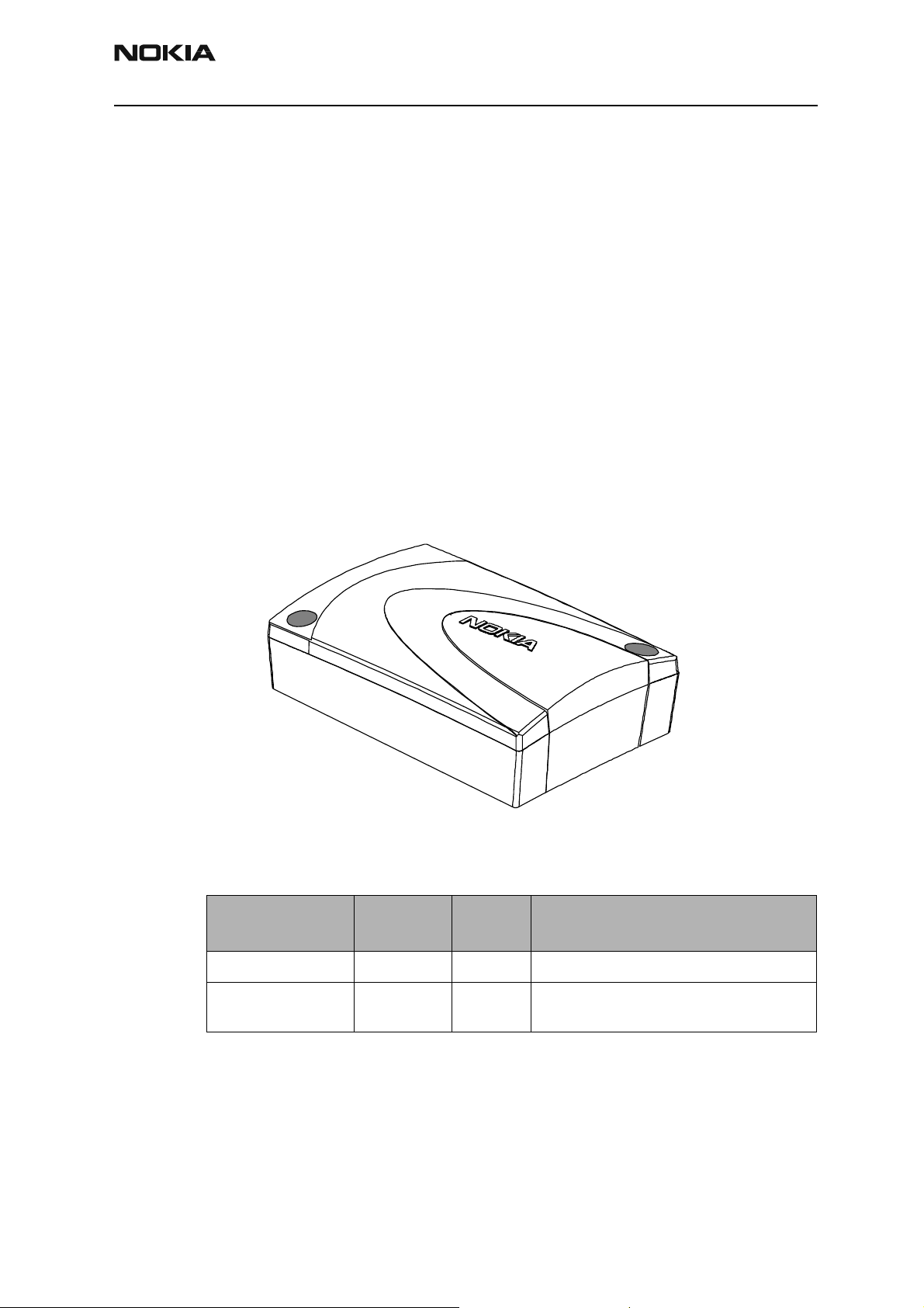
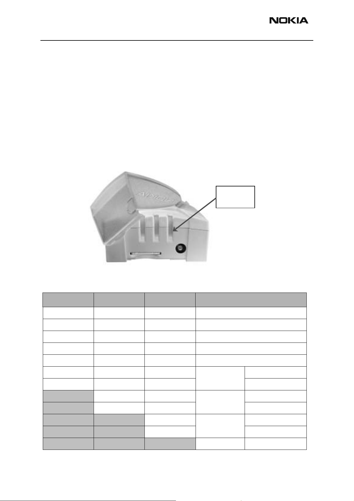
Nokia TME-3 (Nokia 30) is an enhanced GSM900 and GSM 1800 phase 2/2+ type GSM
Connectivity Terminal. The maximum output power in GSM900 system is 2 W (power
class 4 and in GSM1800 1 W (power class 1).
The Nokia 30 GSM Connectivity Terminal is a M2M (machine-to-machine) communications device with versatile interfaces and advanced functions. Connected to different
machines and devices it provides wireless connectivity and remote management possibilities for customer applications. It offers GPRS, USSD, high-speed data, as well as other
advanced services, over EGSM900/GSM1800 networks. It is a perfect fit for various
application environments for its size, vers atility and reliability.
The TME-3 does not include keypad and display, TME-3 user interface comprises three
leds. The leds indicate for example incoming calls and field strength signal level.
Figure 1: Nokia 30 GSM Connectivity Terminal
Product and Module List
Name of module Type code
Transceiver TME-3 0600344
Assembly parts MTME3 0262539 Assembly parts must be ordered as separate
Issue 3 10/03 Nokia Corporation. Page 5
Material
code
Notes
spare parts
Page 12
TME-3 Company confidential
General Information CCS Technical Documentation
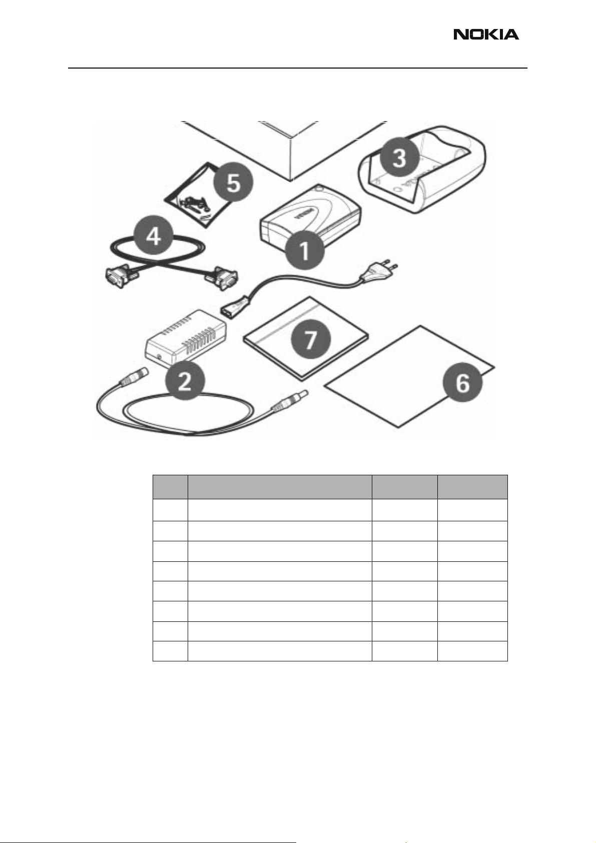
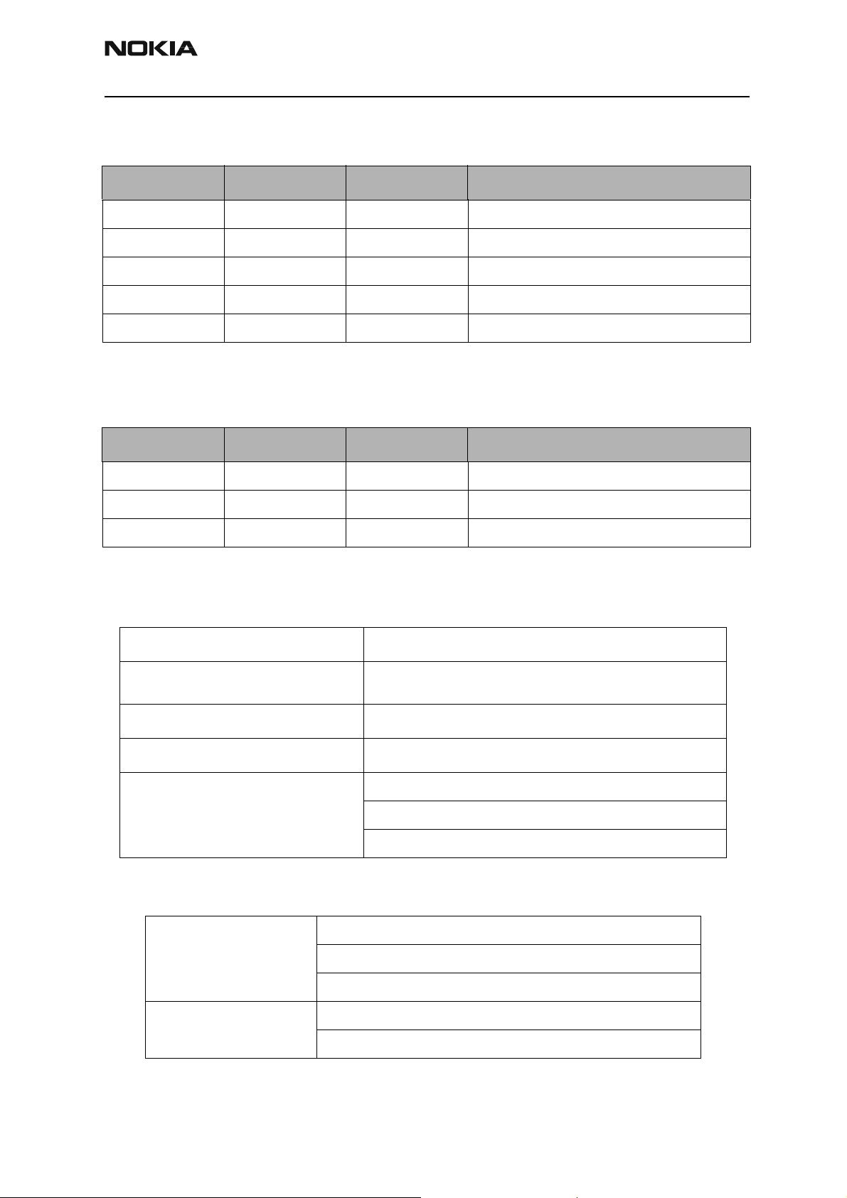
TME-3 with accessories
Figure 2: Product with accessories
8
9
Nokia 30 and accessories:
Item Name Type code Material code
1
2 Power supply unit ACW-5 0630527
3 RS-232 Data adapter DAU-12 0630452
4 RS-232 Data c abl e AXS-3 07 3024 9
5 Nokia 30 installation kit TME-3 0262712
6 Nokia 30 Product Note 9357345
8 Power cable DC 0730244
9 Power cable AC (Eur o ) 0730248
Nokia 30 GSM Connectivity Terminal
TME-3 0600344
Page 6 Nokia Corporation. Issue 3 10/03
Page 13
Company confidential TME-3
CCS Technical Documentation General Information
TME-3/Nokia 30 and accessories:
Item Name Type Code Material code
1. Transceiver TME-3 0600344
Transceiver Amena TME-3 0600345
Transceiver Vodafone TME-3 0600346
Transceiver Movistar TME-3 0600347
Transceiver Czech TME-3 0600358
Transceiver Poland TME-3 0600359
Transceiver Russia TME-3 0600360
Transceiver China TME-3 0600361
Transceiver Turkey TME-3 0600362
Transceiver South Africa TME-3 0600374
Item Chargers Product code:
2. Power supply unit (ACW-5A) 0630527
Power supply unit (ACW-5A) 0675341
DC-power cable (3.0 mm plug) 0730244
AC-power cable (Euro) 0730248
AC-power cable (U.K) 0730247
AC-power cable (U.S.) 0730246
AC-power cable (AS) 0730245
AC-power cable (China) -
Accessories Product code:
3. Data adapter RS-232 (DAU-12) 0630452
4. Data cable RS-232 (AXS-3) 0730249
5 Installation Kit 0262712
6. Nokia 30 Product note (en-ge-fr -sp-r s-hu) 9357345
Nokia 30 Product note (en-tr-pl-ro-bg-uk) 9361026
Nokia 30 Product note (en-fi-sw-it-pr-du ) 9361027
Nokia 30 Product note (en) 9361028
Nokia 30 Product note (en-ch-ch-ch) 9354882
Nokia 30 Product note LSA (en-sp-pr) External antenna cable (XRM-1) 0730262
Issue 3 10/03 Nokia Corporation. Page 7
Page 14
TME-3 Company confidential
General Information CCS Technical Documentation
Technical Specifications
Dimensions
Unit Dimensions (mm) Weigh t (g) Notes
TME-3 terminal 84 x 53 x 26 65 Without Power supply, Data
adapter and Data cab l e
Modes of Ope ration
TME-3 terminal has three operating modes,
• M2M system mode
• AT command mode.
• User control mode
The M2M system mode offers many unique benefits such as wireless bearer selection
(GPRS, USSD, HSCSD, CSD, SMS), ready made protocol stacks, separation of data transfer
from the application and the possibility to introduce new technologies without changing
the application. It offers an open interface for application developers as well as effective
and reliable methods for controlling the terminal and the application.
In the AT command mode the Nokia 30 GSM Connectivity Terminal can be used as a
wireless modem for data and fax communication when attached to a PC. In addition to a
PC, the terminal can be controlled directly by AT commands by PCs and compatible
devices and machines.
In the user control mode the Nokia 30 GSM Connectivity Terminal is controlled by a
mobile phone. Text message templates that are sent from the mob ile to the Nokia 30
instruct the terminal, which in turn controls a device or machine attached to it through
the M2M System connector.
Data transmission
The Nokia 30 GSM Connectivity Terminal supports five bearers for wireless data transfer,
which can be used where GSM networks support them.
· General Packet Radio Service (GPRS)
· High speed circuit switched data (HSCSD)
· Circuit switched data (CSD)
· Short messages (SMS)
· Unstructured Supplementary Service Data (USSD)
Page 8 Nokia Corporation. Issue 3 10/03
Page 15
Company confidential TME-3
CCS Technical Documentation General Information
General Packet Switched Service (GPRS) utilizes packet switched technology where
information is transmitted in small bursts of data. The GPRS mobile station class of the
Nokia 30 is class B. This means that both GPRS connections and circuit switched connections are possible, although it has to be defined which one is used each time. The Nokia
30 supports GPRS multi-slot class 6, thus multiple timeslots can be used for data transfer at the same time: 3 + 1, 2 + 2 or 2 + 1 slots.
RS-232 connection: All wireless bearers can be controlled either with AT in the AT Command mode or with CORBA method calls when the terminal is working in the M2M System mode.
User Interface Features
User Interface consist of LED light indicators that show the state of the TME-3 that is
used to remotely control the Nokia 30. Terminals can also be seen as a user interface.
The small SIM (Subscriber Identity Module) card interface supports 3V SIM cards.
Environmental Conditions
Parameter
Ambient temperature -10 to +55 20 to 75%
Storage temperature -40 to +85 5 to 95%, non condensing
TME-3 is not protected against ingress of water.
Free Fall
TME-3 does not break mechanically after free fall from 100 cm height to concrete floor.
Ambient temperature
(degrees Cels ius)
Ambient humidity
(relative)
Issue 3 10/03 Nokia Corporation. Page 9
Page 16
TME-3 Company confidential
General Information CCS Technical Documentation
User Interface Features
Three light indicators (LEDs) form the user interface of the TME-3.
LED 1 shows the terminal status, while the other two are reserved for the application
module following start-up.
During start-up and special operations, all three light indicators are in terminal use. The
functionality of the light indicators in start-up, normal, and special situations is
described below.
All three LEDs can also be configured so th at they will not show any status and will
remain off during any operation.
Figure 3: UIF LEDs
Led user
interface
Start-up Operation
Table 1: Start-up Operation:
LED 1 LED 2 Status LED Description
- - - Power off / silent mode
Green scan Green scan Green scan Power on, connecting to network
- Red blink - PIN query / new PIN query
- Red blink Red blink PUK query
Intensity of Field Strength:
Red blink - - Non-acceptable <- 105 dB m
Green Blink - - -105 … -100 dBm
Green - - Weak -100 … -95 dBm
Green Green Blink - -95 … -90 dBm
Green Green - Moderate -90 … -85 dBm
Green Green Green Blink -85 … -80 dBm
Green Green Green Good >-80 dBm
Page 10 Nokia Corporation. Issue 3 10/03
Page 17
Company confidential TME-3
CCS Technical Documentation General Information
Normal Operation
Table 2: Normal Operation:
LED 1 LED 2 Status LED Description
* * Green In service
* * Green blink Call on
* * Green blink Incoming call
* * Green/Red blink Message received / Voice mail in box
* * Red blink Message arriving and memory is full
*) Application module controllable in M2M System mode
Special Operation
Table 3: Special Operation:
LED 1 LED 2 Status LED Description
Green/Red blink Green/Red blink Green/Red blink Insert SIM card
Red blink Red blink Red blink Failure, contact service
Yellow Yellow Yellow Initialising
SW features
Basic functionality:
Data features:
GSM supplementary services:
Audio features:
Operation modes
Voice, data, fax, SMS
GPRS Class B,
ETSI GSM phase 2+ Network
Digital/analog audios
M2M System mode
AT Command mode
User Control mode
HSCSD, SMS, USSD
M2M system port
Serial Interfaces
PC software
RS232 system port
WIOP sw
Phoenix service software product specific module
Configurator fo r No kia GSM Connectivity Termi nals
Issue 3 10/03 Nokia Corporation. Page 11
Page 18
TME-3 Company confidential
General Information CCS Technical Documentation
Power supply
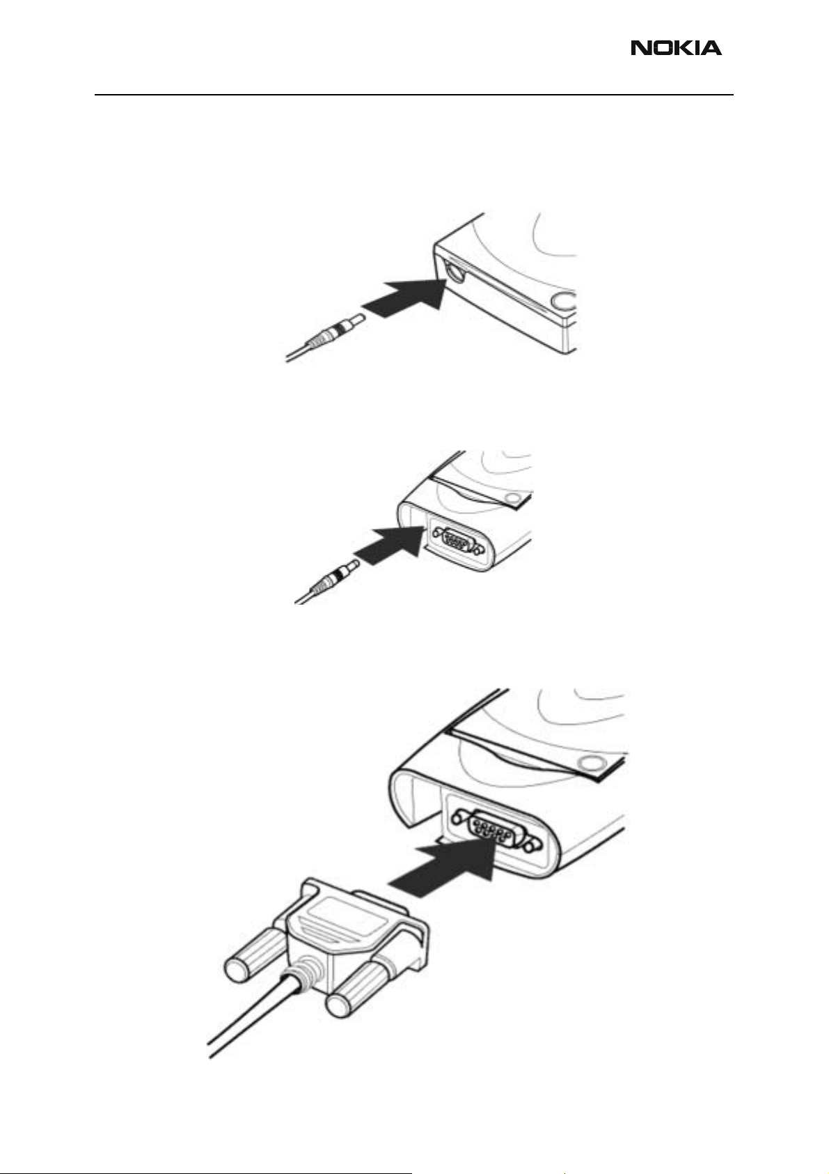
Power supply cord connected to TME-3:
Figure 4: Power to TME-3
With DAU-12 connected the power supply cord is always connected to TME-3
Figure 5: Power supply with DAU-12 connected
Data cable connection
Figure 6: Data cable to DAU-12
Page 12 Nokia Corporation. Issue 3 10/03
Page 19

Programmes After Market Services
TME-3 Series Transceivers
Data Module RL7
Issue 4 12/03 Nokia Corporation.
Page 20

TME-3 Company Confiden tial
Data Module RL7 PAMS Technical Documentation
[This page left intentionally blank]
Page 2 Nokia Corporation. Issue 4 12/03
Page 21

Company Confidential TME-3
PAMS Technical Documentation Data Module RL7
Table of Contents
Page No
Glossary of Terms.......................................................................................................... 5
Functional Description of TME-3.................................................................................. 7
Circuit Description .......................................................................................................7
GSM Data Module RL7................................................................................................. 7
Baseband Module........................................................................................................... 7
Technical Summary .....................................................................................................7
Technical Summary................................................................................................... 8
Modes of Operation .....................................................................................................9
RS232 mode.............................................................................................................. 9
Application mode.................................................................................................... 10
User Control mode.................................................................................................. 10
Internal operation modes......................................................................................... 11
Nominal and maximum ratings .................................................................................12
DC Characteristics................................................................................................... 12
External signals and connectors .................................................................................12
M2M system connector ........................................................................................13
DC connector ........................................................................................................14
SIM connector .......................................................................................................15
External antenna connector ...................................................................................15
Functional Description ...............................................................................................16
POWER................................................................................................................... 16
Power Distribution ................................................................................................16
UEM ......................................................................................................................16
User Interface ........................................................................................................16
UPP Processor .......................................................................................................17
M2M system .........................................................................................................17
SIM .......................................................................................................................17
Audio .........................................................................................................................17
Audio Interfaces...................................................................................................... 18
Earpiece electrical interface .................................................................................... 18
Microphone electrical interface............................................................................... 18
RF Module ................................................................................................................... 19
Normal and extreme voltages for RF block ...............................................................19
DC characteristics ......................................................................................................20
Regulators................................................................................................................ 20
RF characteristics .......................................................................................................22
RF Block Diagram .....................................................................................................23
Frequency synthesizers ........................................................................................... 24
Receiver .....................................................................................................................24
Transmitter .................................................................................................................25
AFC function........................................................................................................... 26
DC-compensation.................................................................................................... 26
Interfaces and Connectors............................................................................................ 27
Antenna ................................................................................................................... 27
User Interface Features............................................................................................ 27
Start-up Operation:.................................................................................................. 27
Normal Operation:................................................................................................... 28
Issue 4 12/03 Nokia Corporation. Page 3
Page 22

TME-3 Company Confiden tial
Data Module RL7 PAMS Technical Documentation
Special Operation:................................................................................................... 28
Data Module RL7 Parts List ........................................................................................ 29
Table of figures
Page No
Fig 1 Block diagram of RL7 module...................................................................................8
Fig 2 TME-3 RS-232 mode .................................................................................................9
Fig 3 TME-3 in Application mode ......................................................................................10
Fig 4 Internal operation modes............................................................................................11
Fig 5 M2M system connector X101 ....................................................................................13
Fig 6 SIM connector X200 .................................................................................................15
Fig 7 External antenna connector X502 ..............................................................................15
Fig 8 TME-3 power distribution..........................................................................................16
Fig 9 Audio control diagram................................................................................................18
Fig 10 RF frequency plan ....................................................................................................19
Fig 11 Power Distribution....................................................................................................21
Fig 12 Phase Locked Loop, PLL .........................................................................................24
List of Schematics, A3 pages
Page No
Block diagram v.RB5.0 ed.76 1
Block Diagram System v.RB5.0 ed.128 2
Schematic diagram RF-BB v.RB5.0 ed.20 3
Schematic Diagram UPP v.RB5.0 ed.26 4
Schematic Diagram UEM v. RB5.0 ed. 77 5
Schematic diagram M2M, PWR, LED v. RB5.0 ed.132 6
Schematic Diagram Memories v. RB5.0 ed.24 7
Schematic Diagram RF, v. RB5.0 ed. 163 8
Diagram of RF ground points, V. RB5.0 ed.34 9
Parts Placement 1/2 RL7_11 10
Parts Placement 2/2 RL7_11 11
Block diagram v.RB6.0 ed.79 12
Block Diagram System v.RB6.0 ed.131 13
Schematic diagram RF-BB v.RB6.0 ed.22 14
Schematic Diagram UPP v.RB6.0 ed.29 15
Schematic Diagram UEM v. RB6.0 ed. 80 16
Schematic diagram AIF, PWR, LED v. RB6.0 ed.135 17
Schematic Diagram Memories v. RB6.0 ed.32 18
Schematic Diagram R FGround points, v. RB6.0 ed. 168 19
Parts placement diagram, RL7_11a top 21
Parts Placement bottom RL7_11a Bottom 22
Page 4 Nokia Corporation. Issue 4 12/03
Page 23

Company Confidential TME-3
PAMS Technical Documentation Data Module RL7
Glossary of Terms
ASIC Application Specific Integrated Circuit
BB Baseband
CSP Chip Scale Package
DB Dual band
DCS1800 Digital Cellular system at 1800 MHz
DSP Digital Signal Processor
EMC Electromagnetic compatibility
EMI Electromagnetic Interference
FBUS Asynchronous Full Duplex Serial Bus
GSM Global System for Mobile communica tions
HSCSD High Speed Circuit Switched Data
LNA Low Noise Amplifier
M2M System Connector
MBUS 1-wire half duplex serial bus
MCU Micro Controller Unit
MDI MCU-DSP Interface
PA Transmit Power Amplifier
PC Personal Computer
PWB Printed Wiring Board
PCM Pulse Code Modulation
PCM SIO Synchronous serial bus for PCM audio transferring
RF Radio Fr equency
SIM Subscriber Identity Module
SMART PCMCIA interface ASIC
Issue 4 12/03 Nokia Corporation. Page 5
Page 24

TME-3 Company Confiden tial
Data Module RL7 PAMS Technical Documentation
UEM Universal Ener gy Management
UI User Interface
UPP Universal Phone Processor
VCXO Voltage Controlled Crystal Oscillator
VCTCXO Voltage Controlled Temperature Compensated Crystal Oscillator.
Page 6 Nokia Corporation. Issue 4 12/03
Page 25

Company Confidential TME-3
PAMS Technical Documentation Data Module RL7
Functional Description of TME-3
Circuit Description
The Data module baseband blocks provide the MCU, DSP, external memory interface and
digital control functions in the UPP ASIC . Power supply circuitry, charging, audio processing and RF control hard ware are in the UEM ASIC.
The purpose of the RF block is to receive and demodulate the radio frequency signal from
the base station and to transmit a modulated RF signal to the base station.
GSM Data Module RL7
The description of the RL7 data module is divided into Baseband and RF sections.
Baseband Module
TME-3 baseband supports a power saving function called "sleep mode". As the M2M system protocol link must be active at all time, only so called "light sleep" is activated intermittently. In this mode the MCU has been shut down but peripherals are active.
TME-3 powered externally and does not have battery and thus there is no need for
charger functions. The power supply is synchronous step down switching type.
Technical Summary
Main functionality of the baseband is implemented into two ASICs: UPP and UEM.
Issue 4 12/03 Nokia Corporation. Page 7
Page 26
TME-3 Company Confiden tial
A
/
A
r
Data Module RL7 PAMS Technical Documentation
Block Diagram
VBATRF
P
O
Voltage
input
AIF_3V3
W
E
VBAT
R
VCCAM VBB
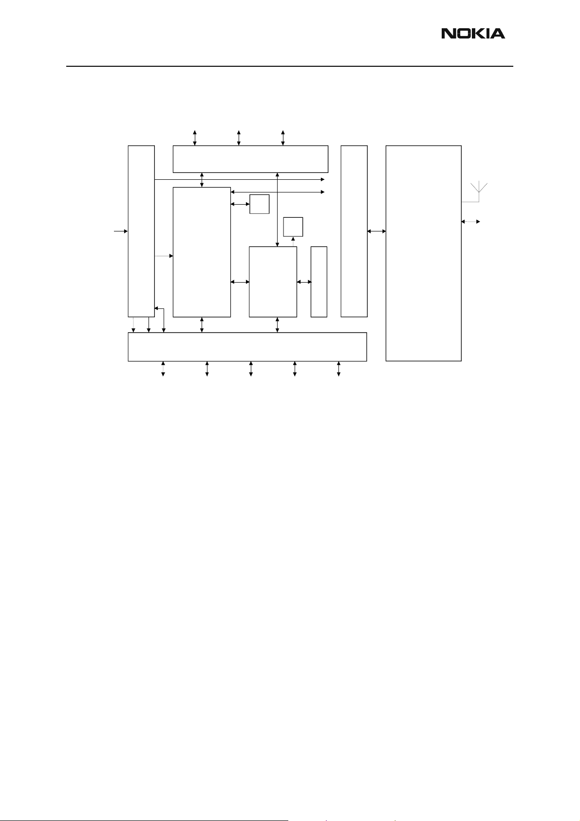
Figure 1: Block diagram of RL7 module
Ostrich
Production
test patte rn
TEST
R&D test
structures
SIM
UI
UEM
UPP
AIF
Internal
RF-
antenna
BB
I
N
T
E
R
F
L
A
S
F
A
C
E
RF
External
antenna
connecto
H
GENIO-
UART
UPP ASIC provides the MCU, DSP, external memory interface and digital control functions. UEM ASIC contains power supply circuitry, charging, audio processing and RF control hardware.
Technical Summary
Baseband is running from power rails 2.8V analog voltage and 1.8V I/O voltage. UPP core
voltage Vcore can be lowered down to 1.0V, 1.3V and 1.5V. UEM includes 6 linear LDO
(low drop-out) regulators for baseband and 7 regulators for RF. It also includes 4 cur rent
sources for biasing purposes and internal usage. UEM also includes SIM interface which
supports 3V SIM cards. TME-3 does not currently support 1.8 V SIMs.
The interface between the baseband and the RF section is handled by a UEM ASIC. The
UEM provides A/D and D/A conversion of the in-phase and quadrature receive and transmit signal paths and also A/D and D/A conversions of received and transmitted audio signals to and from the user interface. The UEM supplies the analog TXC and AFC signals to
RF section according to the UPP DSP digital control.
Data transmission between the UEM and the UPP is implemented using two serial busses, DBUS for DSP and CBUS for MCU. There are also separate signals for PDM coded
audio. Digital speech processing is handled by the DSP inside UPP ASIC. UEM is a dual
voltage circuit, the digital parts are running from the baseband supply 1.8V and the analog parts are running from the analog supply 2.78V. UEM uses also VBAT directly
FBUS
MBUS
NALOG
DIGITAL
UDIO
I/O
Page 8 Nokia Corporation. Issue 4 12/03
Page 27

Company Confidential TME-3
PAMS Technical Documentation Data Module RL7
The baseband supports external microphone inputs and speaker outputs. Input and output signal source selection and gain control is performed by the UEM according to control messages from the UPP. Analog and digital PCM audio are routed to M2M system
connector.
EMC shielding for baseband is implemented using metal lids. On the other side the module is shielded with PWB grounding. Heat generated by the circuitry is conducted out via
the PWB ground planes.
Modes of Ope ration
The TME-3 has three modes of operation:
• RS-232 Mode (M2M sy stem mo de)
• Application mode (AT command mode)
• User Control mode
Internally the RL7 module has the following operating modes:
• NO_SUPPLY
• POWER_OFF
•POWER_ON
• RESET
•SLEEP
• PROTECTION
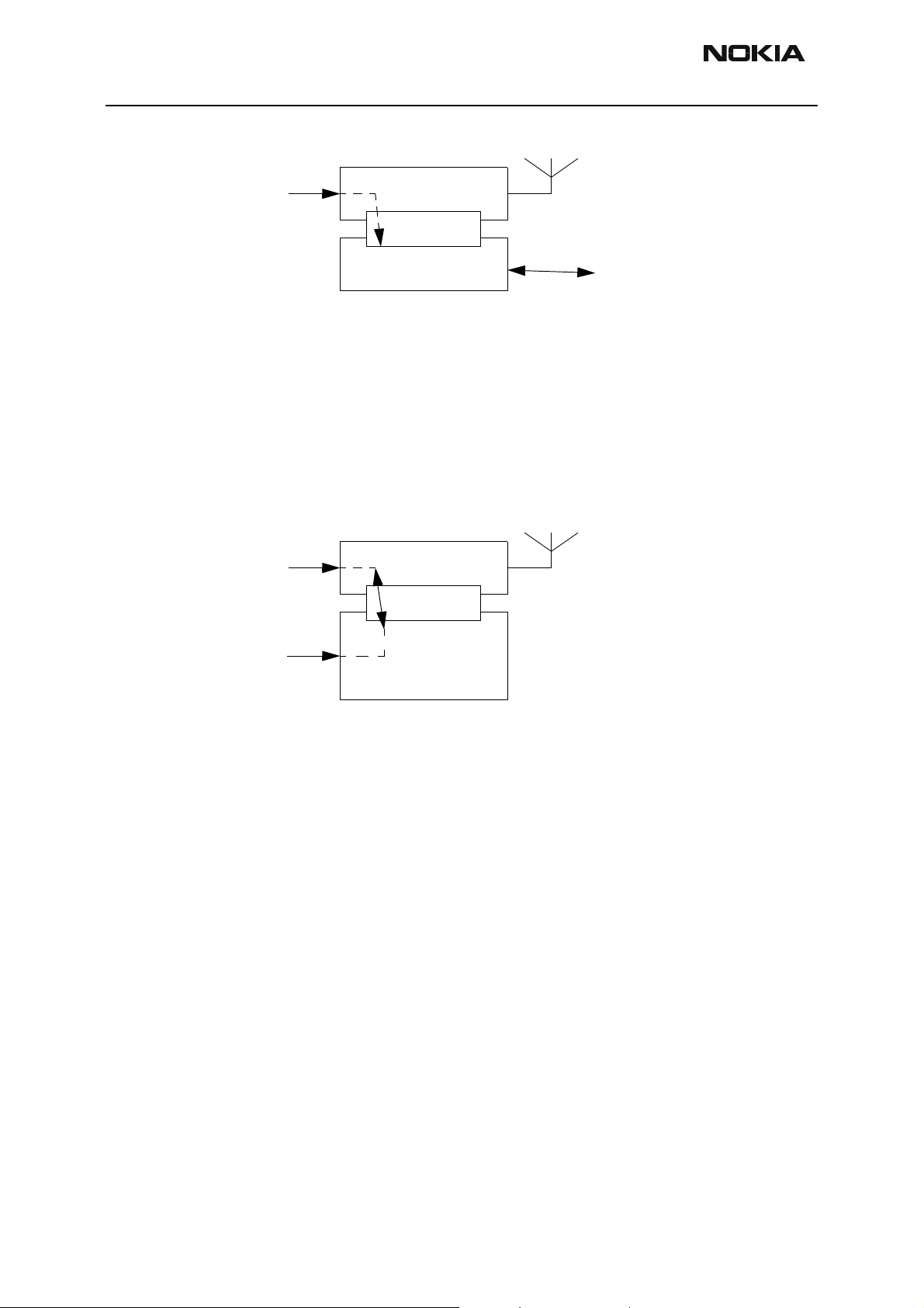
RS232 mode
Fig. 2 shows TME-3 in RS-232 mode. TME-3 enters RS-232 mode in powerup when it
detects a 68k 1% pull-down resistor at M2M system connector pin 21.
In RS-232 mode TME-3 is connected to DAU-12 RS-232 adapter. The adapter provides a
standard RS-232 interface. Power for TME-3 and the adapter is fed through TME-3 DC
jack.
Issue 4 12/03 Nokia Corporation. Page 9
Page 28
TME-3 Company Confiden tial
Data Module RL7 PAMS Technical Documentation
Figure 2: TME-3 RS-232 mode
Voltage input
Application mode
In application mode TME-3 is connected to a user specific application. The mechanical
and electrical interface between application and TME-3 is the M2M system connector.
The application can be powered through M2M system or the application can deliver
power to TME-3.
Voltage input
TME-3
M2M
RS-232 adapter DAU-12
Figure 3: TME-3 in Application mode
TME-3
M2M
RS-232
Alternative voltage
input
User Control mode
In the user control mode the Nokia 30 GSM Connectivity Terminal is controlled by a
mobile phone. Text message templates that are sent from the mob ile to the Nokia 30
instruct the terminal, which in turn controls a device or machine attached to it through
the M2M System connector.
An example of a device attached to the Nokia 30 for wireless control would be a refrigerator. You might want to check the temperature of the refrigerator when out of town.
The temperature of the refrigerator could be altered with the mobile as well.
You could also turn off the lights of the apartment that you had accidentally left on by
sending a text message template.
There are three levels of access control for the User control mode.
Firstly, a message identifier entered when the terminal is used for the first time with the
Nokia 30 Configurator is only known by the person who entered it. This identifier begins
every text message template aimed to control the Nokia 30 and the application attached
to it.
User specific
application
Page 10 Nokia Corporation. Issue 4 12/03
Page 29
Company Confidential TME-3
PAMS Technical Documentation Data Module RL7
Secondly, it can be specified from which phone number the text message templates are
allowed.
Thirdly, a password can be used that is entered whenever a text message template is sent
to the Nokia 30.
Internal operation modes
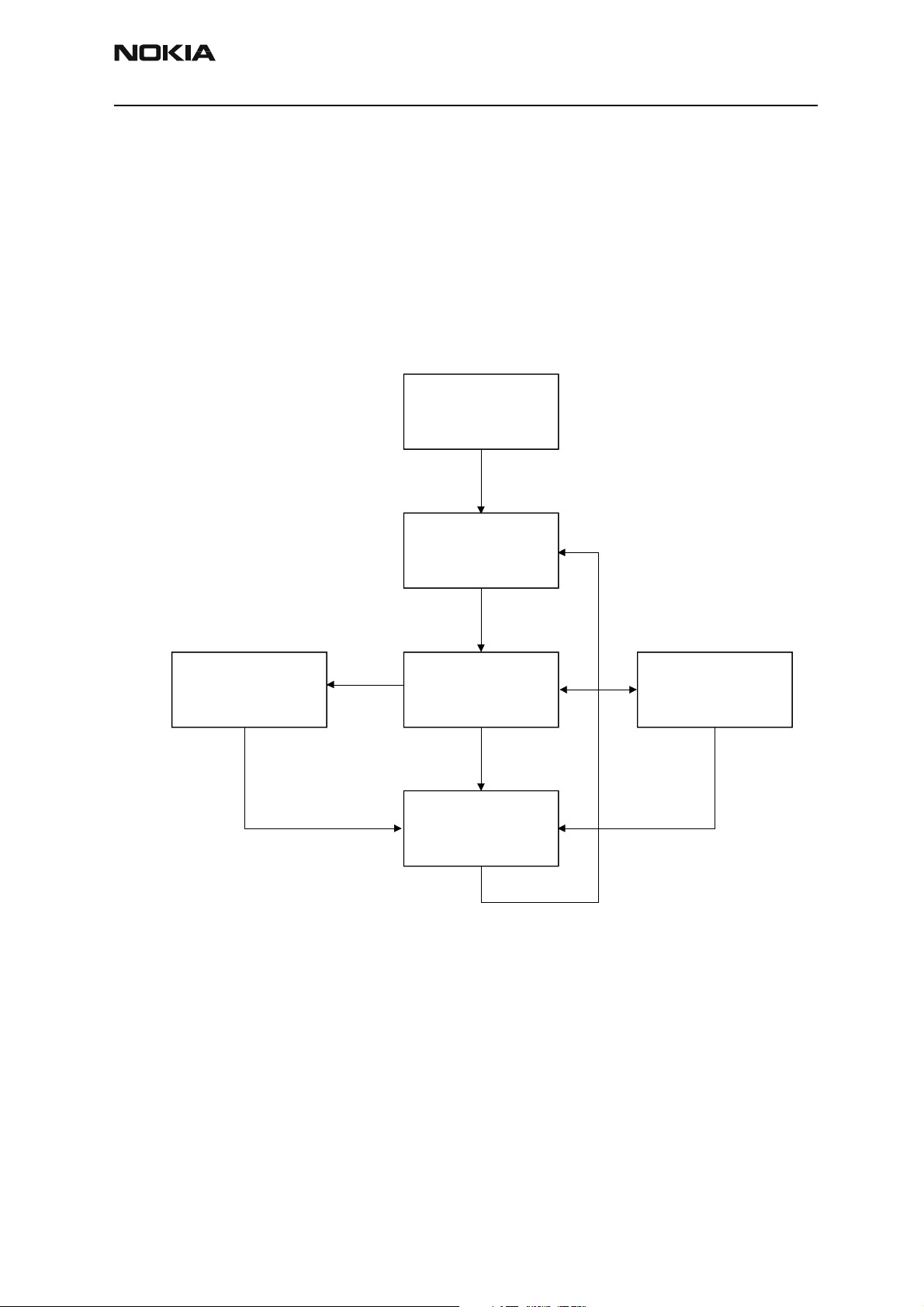
A simplified flow chart of the internal operation modes of TME-3 below.
Figure 4: Internal operation modes
NO_SUPPLY
VBAT
appears
RESET
Thermal
shutdown
POWER_ONPROTECTION SLEEP
Watchdog
bites
Watchdog
bites
POWER_OFF
Always
(forced by HW)
In NO_SUPPLY mode the phone has no supply voltage.
When battery voltage appears, TME-3 enters RESET mode. In TME-3, RESET mode leads
always to POWER_ON mode. During low activity TME-3 can switch f rom POWER_ON to
SLEEP mode. PROTECTION mode happens if the thermal shutdown of UEM regulators
triggers. PROTECTION mode leads immediately to POWER_OFF mode. TME-3 can enter
POWER_OFF mode also from POWER_ON or SLEEP modes if the UEM internal watchdog
elapses. POWER_OFF mode is not stationary.
In TME-3 there is a special power-up hardware, which essentially presses automatically
the power key as soon as it detects the POWER_OFF mode.
Issue 4 12/03 Nokia Corporation. Page 11
Page 30
TME-3 Company Confiden tial
Data Module RL7 PAMS Technical Documentation
Nominal and maximum ratings
Table 1: s
Parameter Absolute Maximum Rating
Supply voltage maximum VBB 15 V
DC input voltage (any signal pin *) -0.5 to 5.5V*
DC output source or sink current
(any signal pin)
Operating temperature range -10...+55 °C
Storage temperature range -40...+85 °C
+/- 10 mA
DC Characteristics
Table 2: Supply volt a ge
Pin / Conn. Line Symbol Minimum
X100 VBB 6.2 V 12.0 V 14.0 V Power feed through
X101/1,3,5,7,9 VBB 4.75 V 12.0 V 15.0 V Power feed trough
Table 3: Power consumption
Mode
Current / mA @
6.7V
Power / W Notes
Typical /
Nominal
Maximum Notes
DC jack
M2M system
POWER_ON, idle < 10 mA < 120mW
POWER_ON, full
load, 900MHz
POWER_ON, full
load, 1800MHz
< 430 mA < 5.2 W Transmitting 2 slots at full power +
< 350 mA < 4.2 W Transmitting 2 slots at full power +
External signals and connectors
This section describes the external and internal electrical connection and interface levels
on the baseband. The electrical interface specifications are collected into tables that
covers a connector or a defined interface.
External connectors comprise the following:
M2M system., DC, SIM, external antenna.
With one green led on; 65 mW
with all leds off.
300 mA @ 3.6 V power feed to M2M
system
300 mA @ 3.6 V power feed to M2M
system
Page 12 Nokia Corporation. Issue 4 12/03
Page 31

Company Confidential TME-3
PAMS Technical Documentation Data Module RL7
M2M system connector
M2M system connector X101 is described below:
Figure 5: M2M system connector X101
The M2M system connector is 50 pin male connector. Connect or connects the TME-3 to
an external applications, for example to the data-adapter. Connection can be made by
female type socket or ribbon cable connector.
Table 4: M2M system connector pinout
Alternate Name Pin Pin Name Alternate
VBB 1 2 GND
VBB 3 4 GND
VBB 5 6 GND
VBB 7 8 GND
VBB 9 10 GND
VCCAM 11 12 Reset
GND 13 14 GENTXD
GENRXD 15 16 GND
RTSAM 17 18 CTSAM
GND 19 20 MBUS
Service 21 22 GND
MIC+ PCMDCLK 23 24 GND
MIC- PCMSCLK 25 26 PCMTX EAR+
GND 27 28 PCMRX EAR-
GND 29 30 FBUSRX
INPUT1 Reserved 31 32 GND
INPUT2 DTR 33 34 FBUSTX
GND 35 36 RTS INPUT3
OUTPUT1 Reserved 37 38 GND
OUTPUT2 DCD 39 40 DSR OUTPUT3
Issue 4 12/03 Nokia Corporation. Page 13
Page 32

TME-3 Company Confiden tial
Data Module RL7 PAMS Technical Documentation
GND 41 42 CTS OUTPUT4
OUTPUT5 RI 43 44 GND
Reserved 45 46 Reserved
GND 47 48 Reserved
Reserved 49 50 GND
in numbering of the M2M system connection
Odd pins are on the left side of the connector, i.e. 1, 3, 5, 7, etc. Even numbers on the
right side of the connector, i.e. 2, 4, 6, 8, etc. Pin 1 is at left top, pin 50 right bottom.
In ribbon cable connection the red stripe conductor of the cable marks pin connection 1.
Conductor numbering is then subsequent from 1 to 50 in the cable
DC connector
DC connector X100, described below, is a 3.2 mm DC jack type connector. VIN is connected to the central pin and the jacket is GND.
Table 5: DC connector pin
Signal Name Pin Notes
GND 3,4
VIN 2 6.2 V – 14.0 V power feed
The connector circuitry composes a 2.0 A fuse and transient protection components.
Power jack tap is a positive (VIN) and border area is a ground (GND).
Page 14 Nokia Corporation. Issue 4 12/03
Page 33

Company Confidential TME-3
PAMS Technical Documentation Data Module RL7
SIM connector
SIM connector X200
cards are not supported.
SIM
C5 C6 C7
C1C2C3
From Battery Type
From SIM Card contact
C8
C4
interface supports both 1.8V and 3V SI M cards. Note t hat 5V SIM
The contacts are described below:
Figure 6: SIM connector X200
GND
UPP
SIMDATA
SIMCLK
SIMRST
VSIM
BSI
SIMCardDet
GND
UEM
SIMIF
register
SIMIO
SIMClk
Data
UEM
digital
logic
SIMIO
SIMClk
Data
UIF Block
UEMInt
CBusDa
CBusEnX
CBusClk
Name Card pin Description
VSIM C1 SIM voltage supply 1.8/3.0V
SIMRST C2 SIM reset
SIMCLK C3 SIM clock
SIMDATA C4 SIM bidirectional data
VPP C5 Unconnected.
GND C7
External antenna connector
External antenna connector X502 interface is used to get better RF sign al in bad
receiving conditions.
Table 6: SIM connector
Figure 7: External antenna connector X502
Issue 4 12/03 Nokia Corporation. Page 15
Page 34

TME-3 Company Confiden tial
Data Module RL7 PAMS Technical Documentation
Functional Description
POWER
TME-3 operates with external DC wall power supply without a battery. The DC voltage
can be supplied either trough the DC jack or the M2M syste m connector. TME-3 has a
wide supply range high efficiency synchronous switched mode step-down converter,
which regulates the input voltage down to normal battery voltage level (3.6V).
Powe r Di st ri b ut i o n
Input voltage from DC connector or M2M system (VBB) is fed to step-down DC-DC converter, which regulates the voltage to 3.6V. The 3.6V is fed to DCT4 power management
circuit UEM (VBAT), to a 3V3 LDO and to the RF power amplifier (VBATRF). UEM regulates
VBAT further for baseband and RF. The 3V3 LDO is used for M2M system I/O buffers.
VBAT is fed to M2M system connector through a switch controlled by UPP.
An application can also draw current directly from the fused input voltage (VBB). The
available current depends on the input voltage and the power consumption of TME-3.
Typical maximum power consumption of TME-3 is less than 5.5 W (including the 300 mA
power feed to the application) in all circumstanc es. For example, if the input voltage is
12.0 V, the application can draw at most 2A - 5.5 W / 12 V = 1540 mA of current without blowing the fuse. However, it is advisable to derate the fuse current to 75% or 1.5 A,
which in the example above leaves ~1000 mA current for the application.
UEM
Figure 8: TME-3 power distribution.
VIN
6.5 V - 8.2 V
DC
Jack
4.75 V - 15.0 V power feed
from AIF
VBB
Power fail
indicator
DC/DC
Step-down
converter
680u
RFC
60R/100M
RFC
60R/100M
To UPP
Power feed/indication
to AIF
3 x 680u
VBAT
3 x 680u
Control
from UPP
VBATRF
LDO
Load switch
3V3
UEM
PA
AIF_3V3
BB
regulators
RF
regulators
300mA power
feed to AIF
AIF
I/O buffers
VCCAM
A
I
F
UEM is an energy management IC. In addition to energy management functionality the
UEM performs all the baseband mixed-signal functions.
User Interface
The TME-3 user interface consist of three two-coloured ( green/red) leds.
Page 16 Nokia Corporation. Issue 4 12/03
Page 35

Company Confidential TME-3
PAMS Technical Documentation Data Module RL7
Six I/O pins from UPP port1, which is normally used for keyboard, are used for led control. Leds are buffered with digital transistors. shows the allocation of led control pins.
Table 7: UI LEDs
BitIO pin # Function Description
P10 LED1 – Green LED Control: 1 = ON, 0 = OFF
P11 LED1 – Red LED Control: 1 = ON, 0 = OFF
P12 LED2 – Green LED Control: 1 = ON, 0 = OFF
P13 LED2 – Red LED Control: 1 = ON, 0 = OFF
P14 LED3 – Green LED Control: 1 = ON, 0 = OFF
P15 LED3 – Red LED Control: 1 = ON, 0 = OFF
The leds are connected between VBAT and ground, and there is a current limiting resistor
and a transistor switch in series with every le d. An 1.8V level active high control signal
from UPP KEYB(10:0) switches the leds on and off. The current through a green led is
~15mA, and the current through a red led is ~5mA. This unsymmetry in led drive currents
ensures that the brightnesses of leds are equal.
UPP Processor
UPP contains ARM7 and LEAD3 MCU & DSP cores, RAM memory and custom logic.
The UPP block contains also an external flash memory. TME-3 flash size is 32Mbit.
M2M system
The M2M system block contains the M2M system connector and the glue logic needed to
make connections between application and the TME-3. The application interface of TME3 is the standard M2M application interfac e. The M2M system interface includes FBUS,
MBUS, GENIOUSART, analog and digital audios (multiplexed to same pins), DC input voltage, regulated 3.6V battery voltage and some general purpose I/Os.
All signal pins of M2M system are 5V tolerant. The 5V input voltage level is translated
down to 2.78V and 1.8V logic levels for UEM and UPP. The outputs of M2M system are
translated from UPP/UEM 1.8V and 2.78V levels to 3.3V level.
M2M system connector is a 50-pin male connector.
SIM
The SIM block contains a SIM card reader, which is connected to UEM SIM interface.
Audio
TME-3 does not have any built-in audio equipment, such as microphone or earpiece.
All audio signals are routed outside of TME-3 via M2M system connector to an external
audio accessory. The RAE-3 does not include or support vibra and buzzer.
Issue 4 12/03 Nokia Corporation. Page 17
Page 36

TME-3 Company Confiden tial
Data Module RL7 PAMS Technical Documentation
The audio control and processing is done by the UEM, which contains the audio codec.
The UPP contains MCU and DSP blocks, handling and processing the audio data signals.
The baseband supports one external microphone input and one external earphone output
or alternatively digital PCM lines.
Audio Interfaces
TME-3 has two different audio types, digital and analog audios. Those lines are multiplexed in M2M system connector, so there is only one physical audio interface.
Figure 9: Audio control diagram
AUDIOSELECT
Audio type selection is made by the audioselect signal from UPP genio pin 28. Audio lines
are multiplexed and demuxed by using NC7SB3157 and these components are controlled
by the audioselect signal
Earpiece electrical interface
Earpiece circuit includes two ferrite beads, two capacitors (27 pF -> 900 MHz cut-off filter) and two varistors for EMC protection. Earphone lines from the M2M system is connected to the differential output (EARP and EARN) in the UEM audio codec.
EARPCMRX
EAR+
PCMTX
AUDIOSELECT
MICPCMSCLK
MIC+
PCMDCLK
AIF 26
AIF 28
MUX 4/2
AIF 23
AIF 25
DEMUX 2/4
Microphone electrical interface
The microphone electrical circuit incl udes EMI/ESD protections which is placed near
the M2M system connector. MICB1 is connected to MIC1P via 1kΩ resistor.
Page 18 Nokia Corporation. Issue 4 12/03
Page 37

Company Confidential TME-3
PAMS Technical Documentation Data Module RL7
RF Module
This RF module executes all RF functions of the module. RF circuitry is located on one
side (B-side) of the PCB.
EMC leakage is prevented by three m etal shields. The first one includes the Bluetooth
module. The second block includes the PA, antenna switch, LNAs and dual RX SAW. The
last block include the Hagar RF IC, VCO, VCTCXO, baluns and balanced filters.
Maximum height inside on RF-shields is 3 mm. Heat generated by t he circuitry will be
conducted out via the PWB ground planes.
Heat generated by the circuitry is conducted out via the PWB ground planes.
Normal and extreme voltages for RF block
There is no extreme voltage due of the internal power block and no battery use.
Parameter Rating
Nominal voltage: 3.6 V (generated in PWR block)
Lower extreme voltage same as nominal
Higher extreme voltage same as nomin al
RF Frequency Plan
Figure 10: RF frequency plan
925-960
MHz
1805-1880
MHz
f
f
f/4
HAGAR
f
f/2f/4
f
f/2
PLL
34203840
MHz
I-signal
I-signalI-signalI-signal
Q-signal
RX
1710-1785
MHz
880-915
MHz
26 MHz
VCTCXO
I-signal
Q-signal
TX
Issue 4 12/03 Nokia Corporation. Page 19
Page 38

TME-3 Company Confiden tial
Data Module RL7 PAMS Technical Documentation
DC characteristics
Regulators
The transceiver comprises a multif unction power management IC on baseband section,
which contains among other functions; 7 pcs of 2.78 V regulators and 4.8V up-switcher
for charge pump.
Use of the regulators can be seen in the Power Distribution Diagram. VrefRF01and
VrefRF02 are used as the reference voltages for HAGAR RF-IC, VrefRF01 (1.35V) for bias
reference and VrfeRF02 (1.35V) for RX ADC's reference.
Regulators (except VR2 and VR7) are connected to HAGAR. Different modes were
switched on by the aid of serial bus.
List of the supply voltages:
Volt. sou rce Load
VR1 PLL charge pump (4,8 V)
VR2 TX modulator
VR3 VCTCXO + buffer
VR4 HAGAR IC (LNAs+mixer+DTOS)
VR5 HAGAR IC (div+LO-buff+prescaler),
VR6 HAGAR (Vdd_bb)
VR7 VCO
VrefRF01 ref. voltage for HAGAR
VrefRF02 ref. voltage for HAGAR
VbattRF PA
Typical current consumption:
Operation mode Current consumption Notes
Pow er OFF < 10 uA Leakage current (d ua l PA)
RX 81 mA, p eak Includes synthesizer current
(28 mA)
TX, without PA 138 mA, peak
TX, power level 5, EGSM900 1700 mA, peak
TX, power level 0, DCS1800 1200 mA, peak
Page 20 Nokia Corporation. Issue 4 12/03
Page 39

Company Confidential TME-3
PAMS Technical Documentation Data Module RL7
Power Distribution Diagram
SOURCE
VR1
VR2
VR3
VR4
VR5
Figure 11: Power Distribution
4.75 V +/- 3.2 %
10 mA
2.78 V +/- 3 %
100 mA
2.78 V +/- 3 %
20 mA
2.78 V +/- 3 %
50 mA
2.78 V +/- 3 %
50 mA
LOAD
Charge pump in HAGAR
TX IQ modulator, pow er
control opamp in
Hagar
VCTCXO
VCTCXO buffer in Haga r
E-GSM & DCS LNA
RX mixer in Hagar
DTOS in Hagar
PLL in Hagar
UEM
VR6
VR7
VrefRF01
VrefRF02
VBATT
2.78 V +/- 3 %
50 mA
2.78 V +/- 3 %
50 mA
1.35 v +/- 1.15 %
< 100 ua
1.35 V +/- 2 %
< 100 ua
3.2 - 4.5 V
1700 mA (max)
Dividers in Hagar
LO buffers in Hagar
Prescaler in Hagar
Power detector
BB section in Hagar
SHF VCO Module
Ref. volt. for Hagar RX
Ref. volt. for Hagar
Dual PA module
Issue 4 12/03 Nokia Corporation. Page 21
Page 40

TME-3 Company Confiden tial
Data Module RL7 PAMS Technical Documentation
RF characteristics
Main RF characteristics are listed in the table below:
Item Values (E-GSM / GSM180 0)
Receive frequency range 925... 960 MHz / 1805...1880 MHz
Transmit frequency range 880... 915 MHz / 1710...1785 MHz
Duplex spacing 45 MHz / 95 MHz
Channel spacing 200 kHz
Number of RF channels 174 / 374
Power class 4 (2 W) / 1 (1 W)
Number of power levels 15 / 16
Transmitter characteristics
Item Values (E-GSM/GSM1800)
Type Dire ct co n ve rs i on, nonlinear, FDMA/TDMA
LO frequency range 3520...3660 MHz / 3420...3570 MHz
Output power 2 W / 1 W peak
Gain control range min. 30 dB
Maximum phase error (RMS/peak) max 5 deg./20 deg. peak
Receiver characteristics
Item Values, E-GSM/GSM1800
Type Direct conversion, Linear, FDMA/TDMA
LO frequencies 3700...3840 MHz / 3610...3760 MHz
Typical 3 dB bandwidth +/- 91 kHz
Sensitivity min. - 102 dBm (GSM1800 norm.cond. only)
Total typical receiver voltage gain
(from antenna to RX ADC)
86 dB
Receiver output level (RF level -95 dBm) 230 mVpp, single-ended I/Q signals to RX
ADCs
Typical AGC dynamic range 83 dB
Accurate AGC co ntrol range 60 dB
Usable input dynamic range -102... -10 dBm
RSSI dynamic range -110... -48 dBm
Page 22 Nokia Corporation. Issue 4 12/03
Page 41

Company Confidential TME-3
PAMS Technical Documentation Data Module RL7
RF Block Diagram
26 MHz
RXI
INP_G_RX
INM_G_RX
Balanced
SAW
RXQ
VCP
VPP
VRF_RX
VLO/VPRE
INP_P_RX
INP_P_RX
VB_EXT
VREF_RX
SLE
SCLK
RESET
HAGAR
LNAB_P
LNAB_G
SDATA
LNA_D
LNA_P
VANT_2
VANT_1
LNA_G
Balanced
SAW
TXP
TXC
DET
VTXLO_P
VPCTRL_P
OUTP_P_TX
OUTM_P_TX
GND
TXIM
RF_TEMP
VTX_B_P
VP_D_SEL
TXIP
VTXLO_G
VPCTRL_G
OUTP_G_TX
OUTM_G_TX
TOUT
TXOP
TXOM
VCTCXO
VTX_B_G
VB_DET
VC_1
VC_2
INP_LO
INM_LO
OUT_CP
Balanced
SAW
MMIC
LNA
MMIC
LNA
Dual SAW
Dual PA
module
Dual
coupler
RX/TX switch
3420 - 3840 MHz
Internal
antenna
RF B l ock Diagram
EGSM900/
GSM1800
Issue 4 12/03 Nokia Corporation. Page 23
Page 42

TME-3 Company Confiden tial
Data Module RL7 PAMS Technical Documentation
Frequency synthesizers
VCO frequency is locked with PLL into stable frequency source, which is a VCTCXO-module. VCTCXO is running at 26 MHz. Temperature drifting is con trolled with AFC voltage.
VCTCXO is locked into frequency of the base station. AFC is generated by baseband with
a 11 bit conventional DAC. 13MHz VCTCXO can also be used if multislot operations is not
needed.
Figure 12: Phase Locked Loop, PLL
26 MHz frequency reference
R
f
ref
f_out /
PHASE
M
DET.
CHARGE
PUMP
AFC-controlled VCTCXO
LP
f_out
VCO
Kd
M
Kvco
M = A(P+1) + (N-A)P=
= NP+A
PLL is located in HAGAR RF-IC and is controlled via serial RFBus. There is 64/65 (P/P+1)
prescaler, N- and A-divider, reference divider, ph ase detector and charge pump for the
external loop filter. SHF local signal, generated by a VCO-module, is fed through a
180deg balanced phase shifter to prescaler. Output of the prescaler is fed to N- and Adivider, which produces the input to phase detector.
Phase detector compares this signal to reference signal (400kHz), which is divided with
reference divider from VCTCXO output. Output of the phase detector is connected into
charge pump, which charges or discharges integrator capacitor in the loop filter depending on the phase of the measured frequency compared to reference frequency.
Loop filter filters out comparison pulses of phase detector and generates DC control voltage to VCO.
Dividers are controlled via serial bus. RFBus Data is for data, RFBusClk is serial clock for
the bus and RFBusEna1X is a latch enable, which stores new data into dividers.
LO-signal is generated by SHF VCO module. VCO has double frequency in GSM1800 and x
4 frequency in EGSM compared to actual RF channel frequency. LO signal is divided by
two or four in HAGAR (depending on system mode).
Receiver
Receiver is a direct conversion, dual band linear receiver. Receiv ed RF-signal from the
antenna is fed via a RF-antenna switch module to the 1st RX bandpass RF-SAW filters
and MMIC LNAs. RF-antenna switch module contains upperband and lowerband opera-
Page 24 Nokia Corporation. Issue 4 12/03
Page 43

Company Confidential TME-3
PAMS Technical Documentation Data Module RL7
tion. The LNA amplified signal is fed to 2nd RX bandpass RF-SAW filters. Both 2nd RX
bandpass RF-SAW filters comprise un-bal/bal configuration to get the balanced (balanced) feed for Hagar.
Discrete LNAs have three gain levels. The first one is max. gain, the second one is about 30dB(GSM1800) and -25dB(EGSM900) below max. gain and the last one is off state. The
gain selection control of LNAs comes from HAGAR IC.
Differential RX signal is amplified and mixed directly down to BB frequency in HAGAR.
Local signal is generated with external VCO. The VCO signal is divided by 2 (GSM1800) or
by 4 (E-GSM900). PLL and dividers are in HAGAR-IC.
From the mixer output to ADC input RX signal is divided into I- and Q-signals. Accurate
phasing is generated in LO dividers. After the mixer DTOS amplifiers convert the differential signals to single ended. DTOS has two gain stages. The first one has constant gain of
12dB and 85kHz cut off frequency. The gain of second stage is controlled wit h contro l
signal g10. If g10 is high (1) the gain is 6dB and if g10 is low (0) the gain of the stage is
-4dB.
The active channel filters in HAGAR provides selectivity for channels (-3dB @ +/-91 kHz
typ.). Integrated base band filter is active-RC-filter with two off-chip capacitors. Baseband filter consists of two stages, DTOS and BIQUAD. DTOS is differential to single-ended
converter having 8dB or 18dB gain. BIQUAD is modified Sallen-Key Biquad.
Integrated resistors and capacitors are tunable. These are controlled with a digital control word. The correct control words that compensate for the process variations of integrated resistors and capacitors and of tolerance of off-chip capacitors are found with the
calibration circuit.
Next stage i n the r eceiv er cha in is a A GC-am plifier, also integrated into HAGAR. AGC has
digital gain control via serial mode bus. AGC-stage provi d es gain control range (40 dB,
10 dB steps) for the receiver and also the necessary DC compensation. Additional 10 dB
AGC step is implemented in DTOS stages.
DC compensation is made during DCN1 and DCN2 operations (controlled via serial bus).
DCN1 is carried out by charging the large external capacitors in AGC stages to a voltage
which cause a zero dc-offset. DCN2 set the signal offset to constant value (VrefRF_02
1.35 V). The VrefRF_02 signal is used as a zero level to RX ADCs.
Single ended filtered I/Q-signal is then fed to ADCs in BB. Input level for ADC is 1.45 Vpp
max.
Transmitter
Transmitter chain consists of two final frequency IQ-modulators fo r upper and lower
band, a dual power amplifier and a power control loop.
I- and Q-signals are generated by baseband. After post filtering (RC-net work) they go
into IQ-modulator in HAGAR. LO-signal for modulator is generated by VCO and is divided
Issue 4 12/03 Nokia Corporation. Page 25
Page 44

TME-3 Company Confiden tial
Data Module RL7 PAMS Technical Documentation
by 2 or by 4 depending on system mode. There are separate outputs one for EGSM and
one for GSM1800.
In EGSM branch there is a SAW filter before PA to attenuate unwanted signals and wideband noise from the Hagar IC.
The final amplification is realized with dual band power amplifier. It has two different
power chains one for EGSM and one for GSM1800. PA is able to produce over 2 W (0
dBm input level) in EGSM band and over 1 W (0 dBm input level) in upperband band into
50 ohm output. Gain control range is over 45 dB to get desired power levels and power
ramping up and down.
Any harmonics generated by the PA are filtered out with filtering in side the antenna
switch -module.
Power control circuitry consists of discrete power detector (common for lower and
upperband) and error amplifier in HAGAR. There is a direction al coupler connected
between PA output and antenna switch. It is a dual band type and has input and outputs
for both systems. Directional coupler takes a sample from the forward going power with
certain ratio. This signal is rectified in a schottky-diode and it produces a DC-signal after
filtering.
The possibility to improve efficiency in low power levels has been specified in power
amplifier module. The improved efficien cy will take place on power level 7 and lower in
EGSM. For this option there is control input line in PA module.
AFC function
AFC is used to lock the transceivers clock to frequency of the base station. AFC-voltage is
generated in BB with 11 bit DA-converter. There is a RC-filter in AFC control line to
reduce the noise from the converter. Settling time requirement for the RC-network
comes from signalling, how often PSW (pure sine wave) slots occur. AFC tracks base station frequency continuously, so transceiver has a stable frequency, because changes in
VCTCXO-output don't occur so fast (temperature).
Settling time requirement comes also from the start up-time allowed. When transceiver
is in sleep mode and "wakes" up to receive mode, there is only about 5 ms for the AFCvoltage to settle. When the first burst comes in system clock has to be settled into +/-
0.1 ppm frequency accuracy. The VCTCXO-module requires also 5 ms to settle into final
frequency. Amplitude rises into full swing in 1... 2 ms, but frequency settling time is
higher so this oscillator must be powered up early enough.
DC-compensation
DC compensation is made during DCN1 and DCN2 operations (controlled via serial bus).
DCN1 is carried out by charging the large external capacitors in AGC stages to a voltage
which cause a zero dc-offset. DCN2 set the signal offset to constant value (RXREF 1.35
V). The RXREF signal is used as a zero level to RX ADCs.
Page 26 Nokia Corporation. Issue 4 12/03
Page 45

Company Confidential TME-3
PAMS Technical Documentation Data Module RL7
Interfaces and Connectors
Antenna
The TME-3 uses an internal or external dual band antenna.
User Interface Features
The TME-3 does not include a display. All UI functions are performed by Leds located in
the A-cover.
*) Application module controllable
Start-up Operation:
Table 8: Start-up Operation:
LED 1 LED 2 Status LED Description
- - - Power off / silent mode
Green scan Green scan Green scan Power on, connecting to network
- Red blink - PIN query / new PIN query
- Red blink Red blink PUK query
Intensity of Field Strength:
Red blink - - Non-acceptable <- 105 dB m
Green Blink - - -105 … -100 dBm
Green - - Weak -100 … -95 dBm
Green Green Blink - -95 … -90 dBm
Green Green - Moderate -90 … -85 dBm
Green Green Green Blink -85 … -80 dBm
Green Green Green Good >-80 dBm
Issue 4 12/03 Nokia Corporation. Page 27
Page 46

TME-3 Company Confiden tial
Data Module RL7 PAMS Technical Documentation
Normal Operation:
Table 9: Normal Operation:
LED 1 LED 2 Status LED Description
* * Green In service
* * Green blink Call on
* * Green blink Incoming call
* * Green/Red blink Message received / Voice mail in box
* * Red blink Message arriving and mem ory is full
*) Application module controllable in M2M System mode
Special Operation:
Table 10: Special Operation:
LED 1 LED 2 Status LED Description
Green/Red blink Green/Red blink Green/Red blink Insert SIM card
Red blink Red blink Red blink Failure, contact service
Yellow Yellow Yellow Initialising
Page 28 Nokia Corporation. Issue 4 12/03
Page 47

Company Confidential TME-3
PAMS Technical Documentation Data Module RL7
Data Module RL7 Parts List
0201802 RL7 RF/Syst Module EDMS Issue: 5.0
Table 11: Parts list RL7_11
Item Code Side Coordinates Part data Part name, type
A1 9517089 Top C 7 RF-SHIELD SHIELD_DMC04003
A3 9517138 Top H 8 RF-SHIELD SHIELD_DMC04002
A4 9517137 Bottom N 5 RF-SHIELD 3 SHIELD_DMC04001
A5 9510791 Top I 4 RF-SHIELD 2 SHIELD_DMC04000
A3 9510729 Top H 8 Lid 4 d md07543
A4 9510728 Bottom N 5 Lid 3 dmd07542
A5 9519722 Top I 1 Lid 2 dmd07511
B200 4510219 Top I 5 32.768KHZ+-30PPM 9PF CRYSTAL_CX_4V
C100 2320805 Bottom J 3 Chipcap X5R 100 N K 10V 0402 0402C
C101 2320805 Bottom L 3 Chipcap X5R 100N K 10V 0402 0402C
C10 2 2320805 Bottom H 3 Chipcap X5R 100N K 10V 0402 0402C
C103 2320805 Top E 1 Chipcap X5R 100N K 10V 040 2 0402C
C104 2320805 Top H 1 Chipcap X5R 100 N K 10V 0402 0402C
C105 2320805 Top H 2 Chipcap X5R 100 N K 10V 0402 0402C
C107 2610039 Bottom M 2 CHIPTCAP 68U M 25V 7.3X4.3X4.1 TANT_TPSE
C109 2320783 Top I 4 Chipcap X7R 33N K 10V 0402 0402C
C110 2320783 Top I 4 Chipcap X7R 33N K 10V 0402 0402C
C111 2320744 Top G 2 Chipcap X7R 10% 50V 0402 0402C
C112 2320744 Top G 1 Chipcap X7R 10% 50V 0402 0402C
C113 232048 1 Bottom L 3 Chipcap X5R 1U K 6V3 0603 0603C
C114 2312243 Bottom K 2 Chipcap X5R 4U7 K 6V3 0805 0805C
C115 2610043 Bottom E 4 CHIPTCAP 680U R 4V0 7.3X4.3X3.8 TA NTAL_D4
C116 2610043 Bottom F 4 CHIPTCAP 680U R 4V0 7.3X4. 3X 3.8 TANT A L_D4
C117 2610043 Bottom F 5 CHIPTCAP 680U R 4V0 7.3X4. 3X 3.8 TANT A L_D4
C118 2320546 Bottom G 3 Chipcap 5% NP0 0402C
C119 2320546 Bottom H 3 Chipcap 5% NP0 0402C
C120 2320 744 Top O 4 Chipcap X7R 10% 50V 0402 0402C
C121 2320805 Top M 4 Chipcap X5R 1 00N K 10V 0402 0402C
C123 2610043 Bottom M 6 CHIPTCAP 680U R 4V0 7.3X4.3X 3.8 TANT A L_D4
Issue 4 12/03 Nokia Corporation. Page 29
Page 48

TME-3 Company Confiden tial
Data Module RL7 PAMS Technical Documentation
Table 11: Parts list RL7_11
Item Code Side Coordinates Part data Part name, type
C124 2610043 Bottom M 8 CHIPTCAP 680U R 4V0 7.3X4.3X 3.8 TANT A L_D4
C126 2360001 Top O 4 Chipcap X5R 330N K 10V 0603 0603C
C127 2320568 Bottom N 7 Chipcap 5% X7R 0402C
C128 2320 744 Bottom N 7 Chipcap X7R 1 0% 50V 0402 0402C
C129 2320 744 Top J 1 Chipcap X7R 10% 50V 0402 0402C
C130 2320 744 Top J 1 Chipcap X7R 10% 50V 0402 0402C
C131 2312243 Top M 5 Chipcap X5R 4U7 K 6V3 0805 0805C
C133 2320568 Top M 1 Chipcap 5% X7R 0402C
C134 2320 744 Top M 1 Chipcap X7R 1 0% 50V 0402 0402C
C135 2320568 Top J 1 Chipcap 5% X7R 0402C
C136 2320 744 Bottom N 2 Chipcap X7R 1 0% 50V 0402 0402C
C137 2610039 Bottom O 2 CHIPTCAP 68U M 25V 7.3X4.3X4.1 TANT_TPSE
C138 2320 744 Bottom M 3 Chipcap X7R 1 0% 50V 0402 0402C
C139 2320568 Bottom I 5 Chipcap 5% X7R 0402 C
C200 2320481 Top H 5 Chipcap X5R 1U K 6V3 0603 0603C
C201 2320 778 Top H 5 Chipcap X7R 10% 16V 0402 0402C
C202 2320481 Top H 5 Chipcap X5R 1U K 6V3 0603 0603C
C203 2320481 Top G 5 Chipcap X5R 1U K 6V3 0603 0603C
C204 2320481 Top I 5 Chipcap X5R 1U K 6V3 0603 0603C
C205 2320536 Top I 5 Chipcap 5% NP0 0402C
C206 2320536 Top I 4 Chipcap 5% NP0 0402C
C20 7 2320481 Top I 3 Chipcap X5R 1U K 6V3 0603 0603C
C208 2320481 Top G 5 Chipcap X5R 1U K 6V3 0603 0603C
C209 2320805 Bottom I 5 Chipcap X5R 100N K 10V 040 2 0402C
C210 232048 1 Bottom I 5 Chipcap X5R 1U K 6V3 0603 0603C
C211 2320805 T o p I 4 Chipcap X5R 100N K 10V 0402 040 2C
C212 2320481 Bottom H 5 Chipcap X5R 1U K 6V3 0603 0603C
C213 2320805 Bottom H 4 Chipcap X5R 100N K 10V 0402 0402C
C214 2320481 Top I 4 Chipcap X5R 1U K 6V3 0603 0603C
C215 2320805 Bottom E 5 Chipcap X5R 100N K 10V 0402 0402C
C216 2320481 Top F 4 Chipcap X5R 1U K 6V3 0603 0603C
C217 2320805 Top G 2 Chipcap X5R 100N K 10V 0402 0402C
Page 30 Nokia Corporation. Issue 4 12/03
Page 49

Company Confidential TME-3
PAMS Technical Documentation Data Module RL7
Table 11: Parts list RL7_11
Item Code Side Coordinates Part data Part name, type
C218 2320805 Top H 2 Chipcap X5R 100 N K 10V 0402 0402C
C219 2320481 Top G 5 Chipcap X5R 1U K 6V3 0603 0603C
C220 2320481 Top G 5 Chipcap X5R 1U K 6V3 0603 0603C
C221 2320805 Top G 2 Chipcap X5R 100N K 10V 0402 0402C
C222 2320481 Top F 5 Chipcap X5R 1U K 6V3 0603 0603C
C223 2320805 Top G 2 Chipcap X5R 100N K 10V 0402 0402C
C224 2320481 Bottom F 4 Chipcap X5R 1U K 6V3 0603 0603C
C225 2320491 Bottom G 5 Chipcap X7R 220N K 10V 060 3 0603C
C226 2320481 Bottom H 6 Chipcap X5R 1U K 6V3 0603 0603C
C227 2320481 Top F 3 Chipcap X5R 1U K 6V3 0603 0603C
C228 2320481 Bottom G 3 Chipcap X5R 1U K 6V3 0603 0603C
C229 2320481 Bottom F 4 Chipcap X5R 1U K 6V3 0603 0603C
C230 2320481 Top F 3 Chipcap X5R 1U K 6V3 0603 0603C
C231 2320481 Bottom G 3 Chipcap X5R 1U K 6V3 0603 0603C
C232 2320 744 Top I 3 Chipcap X7R 10% 50V 0402 0402C
C233 2320 744 Top I 3 Chipcap X7R 10% 50V 0402 0402C
C234 2320 744 Bottom H 3 Chipcap X7R 10% 50V 0402 0402C
C235 2320 744 Top I 3 Chipcap X7R 10% 50V 0402 0402C
C236 2320481 Bottom G 4 Chipcap X5R 1U K 6V3 0603 0603C
C237 2320481 Top F 4 Chipcap X5R 1U K 6V3 0603 0603C
C238 2320481 Bottom H 4 Chipcap X5R 1U K 6V3 0603 0603C
C239 2320481 Top F 5 Chipcap X5R 1U K 6V3 0603 0603C
C240 2320481 Top F 4 Chipcap X5R 1U K 6V3 0603 0603C
C241 2320481 Top F 4 Chipcap X5R 1U K 6V3 0603 0603C
C242 2320481 Bottom G 4 Chipcap X5R 1U K 6V3 0603 0603C
C243 2320481 Bottom G 4 Chipcap X5R 1U K 6V3 0603 0603C
C244 2320481 Top F 3 Chipcap X5R 1U K 6V3 0603 0603C
C246 2320481 Top F 4 Chipcap X5R 1U K 6V3 0603 0603C
C247 2320481 Top H 2 Chipcap X5R 1U K 6V3 0603 0603C
C300 2320805 Top J 3 Chipcap X5R 1 00N K 10V 0402 0402C
C301 2320805 Top J 4 Chipcap X5R 1 00N K 10V 0402 0402C
C302 2320805 Top K 5 Chipcap X5R 100 N K 10V 0402 0402C
Issue 4 12/03 Nokia Corporation. Page 31
Page 50

TME-3 Company Confiden tial
Data Module RL7 PAMS Technical Documentation
Table 11: Parts list RL7_11
Item Code Side Coordinates Part data Part name, type
C303 2320805 Top K 5 Chipcap X5R 100 N K 10V 0402 0402C
C305 2320805 Top K 2 Chipcap X5R 100 N K 10V 0402 0402C
C320 2320 778 Bottom J 5 Chipcap X7R 10% 16V 0402 0402C
C321 2320 778 Bottom J 4 Chipcap X7R 10% 16V 0402C
C322 2320 778 Top I 5 Chipcap X7R 10% 16V 0402C
C323 2320805 Top H 2 Chipcap X5R 100N K 10V 0402C
C324 2320 779 Bottom L 6 Chipcap X7R 100N K 16V 0603_BLM
C400 2320560 Top F 2 Chipcap 5% NP0 0402C
C401 2320560 Top F 2 Chipcap 5% NP0 0402C
C403 2320560 Top H 7 Chipcap 5% NP0 0402C
C500 2320548 Top C 9 Chipcap 5% NP0 0402C
C501 2320546 Top D 9 Chipcap 5% NP0 0402C
C502 2320526 Top E 8 Chipcap +-0.25pF NP0 0402C
C503 2320560 Top E 9 Chipcap 5% NP0 0402C
C504 2320805 Top E 9 Chipcap X5R 100N K 10V 0402C
C505 2320560 Top G 9 Chipcap 5% NP0 0402C
C506 2320560 Top G 9 Chipcap 5% NP0 0402C
C50 7 2320778 Top D 9 Chipcap X7R 10% 16V 0402C
C550 2320536 Top C 8 Chipcap 5% NP0 0402C
C551 2320524 Top D 8 Chipcap +-0.25pF NP0 0402C
C552 2320516 Top E 8 Chipcap +-0.25pF NP0 0402C
C553 2320536 Top E 8 Chipcap 5% NP0 0402C
C554 2320805 Top E 7 Chipcap X5R 100N K 10V 0402C
C555 2320560 Top G 8 Chipcap 5% NP0 0402C
C556 2320560 Top G 8 Chipcap 5% NP0 0402C
C557 2320536 Top D 8 Chipcap 5% NP0 0402C
C600 2320548 Top H 7 Chipcap 5% NP0 0402C
C601 2320554 Top G 8 Chipcap 5% NP0 0402C
C602 2320 778 Top I 7 Chipcap X7R 10% 16V 0402C
C603 2320 778 Top I 8 Chipcap X7R 10% 16V 0402C
C604 2320536 Top I 7 Chipcap 5% NP0 0402C
C605 2320805 Top H 9 Chipcap X5R 100N K 10V 0402C
Page 32 Nokia Corporation. Issue 4 12/03
Page 51

Company Confidential TME-3
PAMS Technical Documentation Data Module RL7
Table 11: Parts list RL7_11
Item Code Side Coordinates Part data Part name, type
C60 7 2314001 Top G 9 Chipcap NP0 470P J 6V3 0402C
C608 2320783 Top I 8 Chipcap X7R 33N K 10V 0402C
C609 2320562 Top I 8 Chipcap 5% NP0 0402C
C610 2320562 T o p I 8 Chipcap 5% NP0 0402C
C611 2320783 Top I 8 Chipcap X7R 33N K 10V 0402C
C612 2320 778 Top I 9 Chipcap X7R 10% 16V 0402C
C613 2320805 Top H 9 Chipcap X5R 100N K 10V 0402C
C614 2320 778 Top I 8 Chipcap X7R 10% 16V 0402C
C615 2320558 Top H 9 Chipcap 5% NP0 0402C
C616 2320552 Top I 7 Chipcap 5% NP0 0402C
C617 2320552 Top I 7 Chipcap 5% NP0 0402C
C620 2320481 Top I 9 Chipcap X5R 1U K 6V3 0603C
C621 2320481 Top I 9 Chipcap X5R 1U K 6V3 0603C
C622 2320481 Top I 9 Chipcap X5R 1U K 6V3 0603C
C623 2320481 Top H 9 Chipcap X5R 1U K 6V3 0603C
C624 2314001 Top H 9 Chipcap NP0 470P J 6V3 0402C
C625 2314001 Top H 9 Chipcap NP0 470P J 6V3 0402C
C626 2314001 Top H 9 Chipcap NP0 470P J 6V3 0402C
C650 2320554 Top K 7 Chipcap 5% NP0 0402C
C652 2320564 Top J 7 Chipcap 5% NP0 0402C
C653 2322015 Top J 6 Chipcap NP0 2N2 G 16V 060 3C
C654 2320564 Top J 6 Chipcap 5% NP0 0402C
C655 2320481 Top K 6 Chipcap X5R 1U K 6V3 0603C
C657 2320520 Top K 7 Chipcap +-0.25pF NP0 0402C
C660 2320560 Top J 8 Chipcap 5% NP0 0402C
C661 2320 779 Top K 8 Chipcap X7R 100 N K 16V 0603_BLM
C662 2320536 Top K 8 Chipcap 5% NP0 0402C
C699 2320518 Top F 7 Chipcap +-0.25pF NP0 0402C
C701 2320548 T o p F 6 Chipcap 5% NP0 0402C
C70 2 2320548 Top F 7 Chipcap 5% NP0 0402C
C703 2320554 Top F 7 Chipcap 5% NP0 0402C
C704 2320516 Top C 4 Chipcap +-0.25pF NP0 0402C
Issue 4 12/03 Nokia Corporation. Page 33
Page 52

TME-3 Company Confiden tial
Data Module RL7 PAMS Technical Documentation
Table 11: Parts list RL7_11
Item Code Side Coordinates Part data Part name, type
C705 2320548 Top F 7 Chipcap 5% NP0 0402C
C706 2320604 Top F 7 Chipcap 5% NP0 0402C
C707 23205 18 To p F 8 Chipcap +-0.25pF NP0 0402C
C709 2312243 Top E 6 Chipcap X5R 4U7 K 6V3 0805C
C710 2320778 Top B 4 Chipcap X7R 10% 16V 0402 0402C
C711 2320548 T o p D 4 Chipcap 5% NP0 0402C
C712 2320778 Top D 4 Chipcap X7R 1 0% 16V 0402 0402C
C713 2320540 T o p E 6 Chipcap 5% NP0 0402C
C714 2320778 Top D 5 Chipcap X7R 1 0% 16V 0402 0402C
C715 2320548 T o p B 5 Chipcap 5% NP0 0402C
C716 2320548 T o p C 7 Chipcap 5% NP0 0402C
C717 2320536 T o p C 8 Chipcap 5% NP0 0402C
C718 2320778 Top C 7 Chipcap X7R 10% 16V 0402C
C719 2320778 Top C 7 Chipcap X7R 10% 16V 0402C
C720 2320 744 Top B 5 Chipcap X7R 10% 50V 0402C
C721 2320536 Top G 9 Chipcap 5% NP0 0402C
C722 2320536 Top G 8 Chipcap 5% NP0 0402C
C723 2320 744 Top G 6 Chipcap X7R 10% 50V 0402C
C724 2320548 Top B 7 Chipcap 5% NP0 0402C
C726 2320508 Top G 7 Chipcap +-0.25pF NP0 0402C
C727 2320546 Top E 5 Chipcap 5% NP0 0402C
C728 2320 778 Top D 5 Chipcap X7R 10% 16V 0402C
C730 2320560 Top I 7 Chipcap 5% NP0 0402C
C731 2320524 Top E 7 Chipcap +-0.25pF NP0 0402C
C751 2320560 Top G 7 Chipcap 5% NP0 0402C
C752 2322023 Top G 7 Chipcap NP0 2N2 J 16V 0603C
C753 2320538 Top D 8 Chipcap 5% NP0 0402C
C754 2320538 Top D 7 Chipcap 5% NP0 0402C
C756 2320546 Top D 8 Chipcap 5% NP0 0402C
C759 2320546 Top C 7 Chipcap 5% NP0 0402C
C780 2320548 Top C 9 Chipcap 5% NP0 0402C
C781 2320548 Top B 9 Chipcap 5% NP0 0402C
Page 34 Nokia Corporation. Issue 4 12/03
Page 53

Company Confidential TME-3
PAMS Technical Documentation Data Module RL7
Table 11: Parts list RL7_11
Item Code Side Coordinates Part data Part name, type
D100 4341053 Bottom I 4 6*BUFFER 1.65V 74LVC07A TSSOP_14
D101 4341053 Bottom F 3 6*BUFFER 1.65V 74LVC07A TSSOP_14
D102 4341307 Bottom I 3 74LVC244 8XBUFFER TSSOP_20
D103 4341243 Top E 1 NC7WZ16 2XBUFFER SC70 -6 SC7 0_6_FAIR
D104 4341307 Bottom J 3 74LVC244 8XBU FFER TSSOP_20
D105 4341245 Top G 1 1XMUX/DEMUX 2:1 NC7SB3157 SC70_6_FAIR
D106 4341245 Top G 1 1XMUX/DEMUX 2:1 NC7SB3157 SC70_6_FAIR
D107 4341245 Bottom H 2 1XMUX/DEMUX 2:1 NC7SB3157 SC70_6_FAIR
D108 4341245 Bottom G 2 1XMUX/DEMUX 2:1 NC7SB3157 SC70_6_FAIR
D200 4370825 Top H 4 UEMK W-DOG ENA TO21 TFBGA168
D300 4370873 Top K 4 UPP8M V2.6 F751986E C035 uBGA144
D320 4340831 Bottom K 4 FLASH 2MX16 1,8V FBGA40
F100 5119002 Top M 2 Fuse 2A 32V SMD 1206_FUSE
F101 5119002 Top K 1 Fuse 2A 32V SMD 1206_FUSE
G650 4350243 Top J 7 VCO 3420-3840MHZ 2.7V 20MA VCO_GK_601MNA_2
G660 4510261 Top J 9 VCTCXO 26MHZ+-5PPM 2.7V GSM VCTCXO_KT16
L100 3203743 Bottom N 1 FERR.BEAD 0R03 42R/100MHZ 3A 0805_BLM21
L101 3203743 Bottom M 5 FERR.BEAD 0R03 42R/100MHZ 3A 0805_BLM21
L102 3203715 Bottom H 2 FERRITE BEAD 0R35 240R/100M FERRITE_BK100 5
L103 3203715 Bottom G 2 FERRITE BEAD 0R35 240R/100M FERRITE_BK1005
L104 3203743 Bottom N 7 FERR.BEAD 0R03 42R/100MHZ 3A 0805_BLM21
L105 3640109 Bottom N 5 CHIP COIL 15U M 2.0A 12.95X9.4X3 COIL_DO3308
L106 3203743 Top N 1 FERR.BEAD 0R03 42R/100MHZ 3A 0805_BLM21
L107 3203743 Top M 1 FERR.BEAD 0R03 42R/100MHZ 3A 0805_BLM21
L108 3203743 Top J 1 FERR.BEAD 0R03 42R/100MHZ 3A 0805_BLM21
L109 3203743 Top J 1 FERR.BEAD 0R03 42R/100MHZ 3A 0805_BLM21
L110 3640475 Bottom O 3 CHOKE 10U M 0R16 1.1A 6.6X4.45 DT1608
L200 3203741 Top F 5 FERRITE BEAD 0R5 600R/100MHZ 0603_BLM
L201 3203741 Top H 5 FERRITE BEAD 0R5 600R/ 100MHZ 0603_BLM
L202 3203741 Top G 5 FERRITE BEAD 0R5 600R/100MHZ 0 0603_BLM
L203 3203741 Top F 5 FERRITE BEAD 0R5 600R/100MHZ 0 0603_BLM
L204 3203741 Top F 4 FERRITE BEAD 0R5 600R/100MHZ 0603_BLM
Issue 4 12/03 Nokia Corporation. Page 35
Page 54

TME-3 Company Confiden tial
Data Module RL7 PAMS Technical Documentation
Table 11: Parts list RL7_11
Item Code Side Coordinates Part data Part name, type
L205 3203741 Top I 2 FERRITE BEAD 0R5 600R/100MHZ 0603_BLM
L500 3646091 Top E 9 CHIP COIL 6N8 J Q27/800M 0402 0402L
L501 3646067 Top G 9 CHIP COIL 18N J Q29/800M 040 2 0402L
L502 3646091 Top D 9 CHIP COIL 6N8 J Q27/800M 0402 0402L
L503 3646065 Top D 9 CHIP COIL 12N J Q31/800M 0402 0402L
L550 3646053 Top E 8 CHIP COIL 4N7 +-0N3 Q28/800M 0402L
L551 3646091 Top G 8 CHIP COIL 6N8 J Q27/800M 040 2 0402L
L552 3646047 Top D 8 CHIP COIL 3N3 +-0N3 Q28/800M 0402L
L700 3646053 Top G 7 CHIP COIL 4N7 +-0N3 Q28/800M 0402L
L701 3646053 Top G 6 CHIP COIL 4N7 +-0N3 Q28/800M 0402L
L702 3646051 Top G 7 CHIP COIL 3N9 +-0N3 Q28/800M 0402L
L703 3203743 Top E 5 FERR.BEAD 0R03 42R/100MHZ 3A 0805_BLM21
L704 3203715 Top B 4 FERRITE BEAD 0R35 240R/100M FERRITE_BK1005
L705 3646059 Top B 4 CHIP COIL 5N6 +-0N3 Q28/800M 0402L
L708 3645065 Top B 6 CHIP COIL 5N6 K Q98/1.5GHZ 0805 0805HQ
L750 4551015 Top C 7 DIR.COUP 897.5/1747.5/1880MHZ COUPLER_LDC15D
N100 4340663 Bottom L 2 LP2985 REG 3.3V 150A SOT23-5 SOT23_5_H1.45
N101 4341217 Top N 4 DC/DC CONTROL (MAX1653) QSOP16_H1.73
N10 2 4341215 Bottom J 5 1XCOMP VREF=1.245 MAX918 SOT23_5_ H1. 45
N600 4370781 Top H 8 HAGAR 5 LFBGA80 uBGA80_H1.7
N700 4350297 Top C 6 PW AMP RF9203E10.1 900/1800
3.5V
R100 1430770 Bottom H 4 Resistor 5% 63mW 0402R
R101 1430770 Bottom H 4 Resistor 5% 63mW 0402R
R10 2 1430770 Bottom H 4 Resistor 5% 63mW 0402R
E5_H1.65
R103 1430770 Bottom I 5 Resistor 5% 63mW 0402R
R104 1430770 Bottom J 4 Resistor 5% 63mW 0402R
R105 1430770 Bottom J 4 Resistor 5% 63mW 0402R
R106 1430770 Bottom G 3 Resistor 5% 63mW 0402R
R107 1430770 Bottom G 3 Resistor 5% 63mW 0402R
R108 1430770 Bottom E 2 Resistor 5% 63mW 0402R
R109 1430770 Bottom G 2 Resistor 5% 63mW 0402R
Page 36 Nokia Corporation. Issue 4 12/03
Page 55

Company Confidential TME-3
PAMS Technical Documentation Data Module RL7
Table 11: Parts list RL7_11
Item Code Side Coordinates Part data Part name, type
R110 1430726 Bottom A 4 Resistor 5% 63mW 0402R
R111 1430740 Bottom A 4 Resistor 5% 63mW 0402R
R112 1430726 Bottom C 4 Resistor 5% 63mW 0402R
R113 1430740 Bottom C 4 Resistor 5% 63mW 0402R
R114 1430726 Bottom B 4 Resistor 5% 63mW 0402R
R115 1430740 Bottom B 4 Resistor 5% 63mW 0402R
R116 1430754 Bottom E 3 Resistor 5% 63mW 0402R
R117 1430770 Bottom J 5 Resistor 5% 63mW 0402R
R118 1430873 Bottom I 5 CHIPRES 0W06 27K F 0402 0402R
R119 1430907 Bottom I 5 CHIPRES 0W06 11K F 0402 0402R
R125 1430 762 Top G 2 Resistor 5% 63mW 0402R
R129 1430 762 Top G 1 Resistor 5% 63mW 0402R
R131 1430 714 Bottom G 3 Resistor 5% 63mW 0402R
R132 1430 714 Bottom G 3 Resistor 5% 63mW 0402R
R134 1414655 Bottom N 7 CHIPRES 0W125 0R10 J 0805 0805R
R135 1430796 Bottom E 2 Resistor 5% 63mW 0402R
R137 1414655 Bottom O 7 CHIPRES 0W125 0R1 0 J 0805 0805R
R141 1430804 To p K 2 Resistor 5% 63mW 0402R
R142 1430 796 Top K 2 Resistor 5% 63mW 0402R
R143 1430 770 Top J 1 Resistor 5% 63mW 0402R
R144 1430121 Top N 5 Chipres 0W06 22k F 200ppm 0402 0402R
R145 1430187 Top N 5 Chipres 0W06 47k F 200ppm 0402 0402R
R146 1825005 Bottom N 1 CHIP VARISTOR VWM14V VC30V 0805_VARISTOR_SIOV
R147 1825033 Bottom H 2 CHIP VARISTOR VW14V VC46V 0402 0402_VAR
R148 1825033 Bottom G 2 CHIP VARISTOR VW14V VC46V 0402 0402_VAR
R149 1430 778 Top E 2 Resistor 5% 63mW 0402R
R150 1430 796 Top O 5 Resistor 5% 63mW 0402R
R151 1430690 Top J 2 Chipres 0W06 jumper 0402 0402R
R153 1430 770 Top I 3 Resistor 5% 63mW 0402R
R154 1430 796 Top I 3 Resistor 5% 63mW 0402R
R155 1430770 Bottom K 3 Resistor 5% 63mW 0402R
R156 1430911 Top I 2 Resistor 1% 63mW 0402R
Issue 4 12/03 Nokia Corporation. Page 37
Page 56

TME-3 Company Confiden tial
Data Module RL7 PAMS Technical Documentation
Table 11: Parts list RL7_11
Item Code Side Coordinates Part data Part name, type
R157 1430911 Top I 2 Resistor 1% 63mW 0402R
R158 1430911 Top J 3 Resistor 1% 63mW 0402R
R159 1430911 Top I 2 Resistor 1% 63mW 0402R
R160 1430911 Top I 3 Resistor 1% 63mW 0402R
R161 1430911 Top I 3 Resistor 1% 63mW 0402R
R162 1430726 Bottom H 2 Resistor 5% 63mW 0402R
R163 1430726 Bottom G 2 Resistor 5% 63mW 0402R
R164 1430690 Top O 4 Chipres 0W06 jumper 0402 0402R
R202 1620067 Top I 3 RES NETWORK 0W06 4X1 00K J MNR0804
R204 14302 15 Top J 3 CHIPRES 0W06 68K F 200PPM 0402R
R205 1430790 Bottom G 3 Resistor 5% 63mW 0402R
R206 4120071 Bottom A 6 ASIP EMIF03-SIM01 SIM FILTER uBGA8
R20 7 1430778 Bottom H 6 Resistor 5% 63mW 0402R
R320 1430770 Bottom L 6 Resistor 5% 63mW 0402R
R400 1430 778 Top F 2 Resistor 5% 63mW 0402R
R401 1430 778 Top F 2 Resistor 5% 63mW 0402R
R403 1430 726 Top H 7 Resistor 5% 63mW 0402R
R500 1430 726 Top E 9 Resistor 5% 63mW 0402R
R501 1430 700 Top E 9 Resistor 5% 63mW 0402R
R502 1430832 To p D 9 Resistor 5% 63mW 0402R
R520 1430830 Bottom D 2 Resistor 5% 63mW 0402R
R551 1430 700 Top E 7 Resistor 5% 63mW 0402R
R558 1430832 To p D 8 Resistor 5% 63mW 0402R
R600 1620081 Top I 9 RES NETWORK 0W03 4X22R J 0804 MNR04
R602 1430 770 Top I 9 Resistor 5% 63mW 0402R
R603 1430846 To p G 8 Resistor 1% 63mW 0402R
R604 1430 770 Top H 9 Resistor 5% 63mW 0402R
R606 1430 784 Top H 9 Resistor 5% 63mW 0402R
R60 7 1620033 Top I 7 RES NETWORK 0W06 2X5K6 J 0404 0404_R
R608 1620033 To p I 7 RES NETWORK 0W06 2X5K6 J 0404 0404_R
R610 1430700 Top I 7 Resistor 5% 63mW 0402R
R650 1430137 Top J 6 CHIPRES 0W06 1K0 F 200PPM 0402 0402R
Page 38 Nokia Corporation. Issue 4 12/03
Page 57

Company Confidential TME-3
PAMS Technical Documentation Data Module RL7
Table 11: Parts list RL7_11
Item Code Side Coordinates Part data Part name, type
R651 1430907 Top J 6 CHIPRES 0W06 11K F 0402 0402R
R652 1430 700 Top K 7 Resistor 5% 63mW 0402R
R660 1430 762 Top J 8 Resistor 5% 63mW 0402R
R661 1430 774 Top K 8 Resistor 5% 63mW 0402R
R700 1620121 Top G 7 RES NETWORK 0W06 2X220R J MNR02_SR 0404
R701 1620121 Top F 7 RES NETWORK 0W06 2X22 0R J MNR02_SR 0404
R703 1430 714 Top D 7 Resistor 5% 63mW 0402R
R704 1430 718 Top C 7 Resistor 5% 63mW 0402R
R705 1620515 Top C 4 RES NETWORK 0W04 1DB ATT 0404_RAC10
R706 1430693 Top G 6 Chipres 0W06 5R6 J 0402 0402R
R707 1430693 Top G 7 Chipres 0W06 5R6 J 0402 0402R
R709 1430 734 Top B 7 Resistor 5% 63mW 0402R
R751 1430 770 Top D 7 Resistor 5% 63mW 0402R
R752 1430 788 Top H 7 Resistor 5% 63mW 0402R
R753 1430 770 Top D 8 Resistor 5% 63mW 0402R
R754 1430 726 Top D 7 Resistor 5% 63mW 0402R
R755 1430 718 Top C 8 Resistor 5% 63mW 0402R
R756 1430 770 Top H 6 Resistor 5% 63mW 0402R
R757 1430 778 Top D 7 Resistor 5% 63mW 0402R
R780 1430 700 Top B 9 Resistor 5% 63mW 0402R
R781 1430 700 Top B 9 Resistor 5% 63mW 0402R
T650 3640423 Top I 8 BALUN TRANS 3.7GHZ+/-300MHZ TRANS_LDB15 0805
T700 4550137 Top F 7 TRANSF BALUN 1.8GHZ+-100MHZ TRANS_LDB15 2x1.3
V100 4864511 Top A 7 LED MUW GRN/RED 570/620NM LED_SML_521
V101 4864511 Top A 5 LED MUW GRN/RED 570/620NM LED_SML_521
V102 4864511 Top A 4 LED MUW GRN/RED 570/620NM LED_SML_521
V103 4210043 Bottom B 4 TR DTC1 43ZE RB=4K 7 RBE=47K EM3
V104 4210043 Bottom C 4 TR DTC1 43ZE RB=4K 7 RBE=47K EM3
V105 4210043 Bottom C 4 TR DTC1 43ZE RB=4K 7 RBE=47K EM3
V106 4210043 Bottom A 4 TR DTC143ZE RB=4K7 RBE=47K EM3
V107 4210043 Bottom B 4 TR DTC143ZE RB=4K7 RBE=47K EM3
V108 4210043 Bottom A 4 TR DTC143ZE RB=4K7 RBE=47K EM3
Issue 4 12/03 Nokia Corporation. Page 39
Page 58

TME-3 Company Confiden tial
Data Module RL7 PAMS Technical Documentation
Table 11: Parts list RL7_11
Item Code Side Coordinates Part data Part name, type
V109 4110074 Bottom O 1 SCH DI 40V 3A SOD6
V110 411007 8 Top M 4 SLHDIx2 70mA SO T323
V111 4211321 Bottom M 3 MFET FDS6912A N 30V 6A 0R035 SO8N2
V112 4211391 Top K 1 MFET P FDC6323L SWITCH 3-8V TSOP_6
V114 4110074 Bottom M 5 SCH DI 40V 3A SOD6
V115 4110078 Top E 2 SLHDIx2 70mA SOT323
V120 4110078 Bottom K 3 SLHDIx2 70mA S OT323
V200 4219926 Bottom I 5 TR+RX2 RN1302 N 50V 50MA 10K SOT323
V201 4219926 Bottom H 5 TR+RX2 RN1302 N 50V 50MA 10K SOT323
V500 4210277 Top D 9 TR BGB420 MIRROR ADJ BIAS SOT343_R
V550 4210261 Top D 8 TR BGA428 LNA1.8GHZ 19.5DB SOT_363
V750 4110079 Top D 7 SCH DIX2 HSMS282C 15V <1PF SOT323
X100 5409003 Top N 2 SMD JACK 3.0MM F DC 9V 1A SMK_JACK_SWITCH
X101 5400225 Bottom H 1 SM PIN HEADER 2X25M P1.27MM
STR
X200 5409201 Bottom C 6 SM SIM CONN 2X3POL SK51002_001
X502 5429017 Bottom C 3 SM CONN RF PLUG+SW 3GHZ 1W
90DEG
Z100 4120051 Top I 1 EMI ESD FILT10CH IP4026CX25 uBGA_25_P0.75
Z101 4120051 Top F 1 EMI ESD FILT10CH IP4026C X2 5 uBGA_25_P0.75
Z500 4512133 Top B 8 ANT.SWIT.880-960/1710-1990MHZ 7x5 UM_0318C1
Z501 4511235 Top F 9 SAW FILT 942.5+-17.5MHZ/3.8DB 3x3 DCC6D_H1.15
Z520 4511 181 Top D 9 Filter SAW 925-960/1 80 5-1880
MHZ
Z551 4511241 Top F 8 SAW FILT 1842.5+-37.5MHZ/3.5DB 3x3 DCC6D_H1.15
Z700 4511237 Top F 7 SAW FILT 897.5+-17.5MHZ/4.2DB 3x3 DCC6D_H1.15
SAMTEC_ASP_67923_0
2
SWITCH_SHALTER
QCC8B_4.0X4.0
Page 40 Nokia Corporation. Issue 4 12/03
Page 59

Programmes After Market Services
TME-3 Series Transceivers
Variants
Issue 3 10/03 Nokia Corporation.
Page 60

TME-3 Company confidential
Variants CCS Technical Documentation
[This page left intentionally blank]
Page 2 Nokia Corporation. Issue 3 10/03
Page 61

Company confidential TME-3
CCS Technical Documentation Variants
Table of Contents
Page No
Variants of TME-3......................................................................................................... 4
TME-3 Exploded Diagram............................................................................................. 6
TME-3 Assembly Parts List ........................................................................................7
Issue 3 10/03 Nokia Corporation. Page 3
Page 62

TME-3 Company confidential
Variants CCS Technical Documentation
Variants of TME-3
Name Type des. Code
Transceiver TME-3 0600344
Transceiver Amena TME-3 0600345
Transceiver Vodafone TME-3 0600346
Transceiver Movistar TME-3 0600347
Transceiver Czech TME-3 0600358
Transceiver Poland TME-3 0600359
Transceiver Russia TME-3 0600360
Transceiver China TME-3 0600361
Transceiver Turkey TME-3 0600362
Transceiver South Africa TME-3 0600374
Transceiver PT-2 TME-3 0600381
Page 4 Nokia Corporation. Issue 3 10/03
Page 63

Company confidential TME-3
CCS Technical Documentation Variants
[This page left intentionally blank]
Issue 3 10/03 Nokia Corporation. Page 5
Page 64

TME-3 Company confidential
Variants CCS Technical Documentation
TME-3 Exploded Diagram
The following picture shows the exploded view of TME-3. The numbers in the followings
sections refer to this picture.
1
2
3
4
5
For reassembly refer to the Troubleshooting section of this manual.
Page 6 Nokia Corporation. Issue 3 10/03
Page 65

Company confidential TME-3
CCS Technical Documentation Variants
TME-3 Assembly Parts List
More information in section Troubleshooting.
Part N umber in
Exploded View
1 1 9452113 SIM card cover DMD08007
2 1 9452093 A-cover DMD08005
3 1 0660256 Antenna
5 1 9459140 B-cover DMC06617
6 2 6293005 PT-screw (not shown) k22x8
Pcst Material Code Part Name Type
Issue 3 10/03 Nokia Corporation. Page 7
Page 66

TME-3 Company confidential
Variants CCS Technical Documentation
[This page left intentionally blank]
Page 8 Nokia Corporation. Issue 3 10/03
Page 67

Customer Care Solutions
TME-3 Series Transceivers
Service Software Instructions
Issue 3 10/03 Copyright Nokia. All rights reserved..
Page 68

TME-3 Company confidential
Service Software Instructio ns CCS Technical Documentation
[This page left intentionally blank]
Page 2 Copyright Nokia. All rights reserved.. Issue 3 10/03
Page 69

Company confidential TME-3
CCS Technical Documentation Service Software Instructions
Table of Contents
Page No
Service Software Instructions for TME-3...................................................................... 5
Before Installation .......................................................................................................5
Dongle driver installation and version check................................................................. 6
First time installation of Phoenix................................................................................... 8
TME-3 Service Software Installation procedure ......................................................... 11
Startup ........................................................................................................................12
Update Installation of Phoenix..................................................................................... 13
How to uninstall Phoenix ...........................................................................................14
Data package for Phoenix (product specific)............................................................... 16
Before installation ......................................................................................................16
Installation of Phoenix Data Package (Product Specific) ..........................................17
How to Uninstall Data Package .................................................................................20
How to Manage Connections .....................................................................................21
Manual Settings....................................................................................................... 22
A) For FLS-4S POS Flash Device choose following connection settings ...........22
B) For FPS-8 Flash Prommer choose following connection settings: ..................22
How to Update Flash Support Files for FPS-8* and FLS-4* ...................................... 24
Before Installation .....................................................................................................24
Installing the Flash Support Files ..............................................................................24
How to Update The FPS-8* Flash Prommer SW ......................................................27
FPS-8 Activation and Deactivation.............................................................................. 29
Activation ..................................................................................................................29
Deactivation ...............................................................................................................30
JBV-1 Docking Station SW......................................................................................... 31
Before Installation .....................................................................................................31
Installing SW Needed for the JBV-1 SW Update .....................................................32
Updating the JBV-1 Docking Station Software .........................................................36
TME-3 specific menus in Phoenix............................................................................... 38
Light Indicators ..........................................................................................................39
Main functionality .................................................................................................39
M2M System Connector ............................................................................................40
Remote I/O Control & Audio settings .......................................................................41
Hardware setup instructions......................................................................................... 42
Flash Concept ............................................................................................................42
Point of sale (POS) flashing concept .........................................................................43
Jig Concept ................................................................................................................44
JBV-1 Flash Concept .................................................................................................45
JBV-1 Service Concept ..............................................................................................46
Service Box SB-1 set-up ............................................................................................47
Issue 3 10/03 Copyright Nokia. All rights reserved.. Page 3
Page 70

TME-3 Company confidential
Service Software Instructio ns CCS Technical Documentation
Service Software Instructions for TME-3
Phoenix is the Nokia Test and Service Software for mobile phones.
Figure 1: Phoenix
Before Installation
• Install the Phoenix Service SW A
• Install the TME-3 Phoenix Service SW
• Install the Data Package for Phoenix (product specific data and flash update
package)
• Manage connection settings (depends on the tools you are using)
• Update FPS-8 SW (if you use FPS-8).
•
Activate FPS-8
• Update JBV-1 Docking Station SW (only when needed
The flash update files are delivered with then Phoenix Data Package so unless you want
to use certain version of this package, separate installation package is not needed any-
more. If you want to use it, it should be installed after connection management, before
FPS-8 update.
Refer to Service Manual and Technical Bulletins for more information concerning phone
model specific tools and equipment setup.
Page 4 Copyright Nokia. All rights reserved.. Issue 3 10/03
Page 71

Company confidential TME-3
CCS Technical Documentation Service Software Instructions
Dongle driver installation and version check
If there is no previously installed Dongle driver, installation will take place….
Figure 2: Dongle driver installation window
If the Dongle driver is installed and it is older than the latest supported version, the latest
version will be installed when you choose “Yes”. The latest version is always included in
the latest Phoenix installation package.
Figure 3: Dongle driver update window
PC needs to be rebooted before installation can continue. Click “Yes” to reboot the PC
Setup is restarted automatically after reboot..
Figure 4: Dongle driver update completed window
If at any point during installation you get this message, the Dongle is not found and
Issue 3 10/03 Copyright Nokia. All rights reserved.. Page 5
Page 72

TME-3 Company confidential
Service Software Instructio ns CCS Technical Documentation
installation can’t continue..
Figure 5: Error message at pre-installation
Possible reasons may be defective or too old PKD-1Dongle (five digit serial number Don-
gle when used whit FPS-8 Prommer) or that the FLS-4S POS Flash Dongle is defective or
power to it is not supplied by external charger.
Check the COM/parallel ports used first! After correcting the problem Installation can be
restarted
Page 6 Copyright Nokia. All rights reserved.. Issue 3 10/03
Page 73

Company confidential TME-3
CCS Technical Documentation Service Software Instructions
First time installation of Phoenix
After Dongle driver installation / update (if needed) installation continues from this step.
If the Phoenix Service Software A is already installed proceed to p.11
Click “Next” in Welcome dialog to continue.
Figure 6: Welcome dialog
Choose the destination folder, it is recommended to use the default folder C:\Program
Files\Nokia\Phoenix.
Choose “Next” to continue. Y ou may choose another location by selecting “Browse” (not
Issue 3 10/03 Copyright Nokia. All rights reserved.. Page 7
Page 74

TME-3 Company confidential
Service Software Instructio ns CCS Technical Documentation
recommended)
Figure 7: File location window
Setup copies the components, please wa it.
Progress of the setup is shown. Please wait…
Figure 8: Setup status window
If restarting of your computer is needed the Install Shield Wizard will tell you about it.
Select “Yes…” to reboot the PC immediately and “No…” to reboot the PC manually.
Page 8 Copyright Nokia. All rights reserved.. Issue 3 10/03
Page 75

Company confidential TME-3
CCS Technical Documentation Service Software Instructions
Note that Phoenix doesn’t work, if components are not registered. Click “Finish” to con-
tinue. .
Figure 9: Installation complete -window
After the reboot components are registered and Phoenix is ready for use.
If reboot is not needed components are registered after copying them.
Figure 10: Registering window
Phoenix is now ready for use.
Now the installation of Phoenix Service SW is ready and it can be used for TME-3 after:
• Installing TME-3 specific Phoenix Service SW as follow the instructions “First
Time Installation Of Phoenix”
• Installing Phone model specific Phone Data Package for Phoenix
• Configuring the connections
• Updating the Flash Update Package files used with FPS-8* tool
Issue 3 10/03 Copyright Nokia. All rights reserved.. Page 9
Page 76

TME-3 Company confidential
Service Software Instructio ns CCS Technical Documentation
TME-3 Service Software Installation procedure
• Check that a Dongle is attached to the parallel port of your computer.
• Download the latest installation package (e.g.
phoenix_service_sw_a3_03_83_005.exe) to your comp uter (e.g.:\TEMP)
• Close all other programs
• Install Phoenix by executing the Phoenix installation package and follow the
instructions on the screen.
• Download the latest release (e.g. TME-3_03_83_010.exe). Please contact
your regional After Market Service point for information on where to download
the latest release.
• Run the application file (e.g. TME-3_03_83_010.exe) and follow instructions
on the screen
• Administrator rights may be required to be able to install Phoenix depending
on the Operating System
• If the dongle driver is installed or updated, you need to reboot your PC before
the installation can continue.
• If uninstalling or rebooting is needed at any point, you will be prompted by the
install Shield program.
Page 10 Copyright Nokia. All rights reserved.. Issue 3 10/03
Page 77

Company confidential TME-3
CCS Technical Documentation Service Software Instructions
Startup
Run the phoenix_service_sw_a3_03_83_005.exe to start installation.
When you choose “Next” the files needed for installation will be extracted.
Kindly wait.
Figure 11:
If the setup files are already extracted (left in the file system from previous installation)
following dialog appears. Always click “Yes to All” to overwrite the existing setu p files
Figure 12: Overwrite protection
Issue 3 10/03 Copyright Nokia. All rights reserved.. Page 11
Page 78

TME-3 Company confidential
Service Software Instructio ns CCS Technical Documentation
Update Installation of Phoenix
If you already have the Phoenix Service SW installed on your computer, sooner or later
there will be need to update it when new versions are released.
Please note that very often the Phoenix Service SW and the Phone Specific Data Package
for Phoenix come in pairs, meaning that certain version of Phoenix can only be used with
certain version of Data Package. Always use the latest available versions of both. Instructions can be found in phone model specific Technical Bulletins.
To update the Phoenix you need to take exactly the same steps as when installing it for
the first time.
• Download the installation package to your computer hard disk
• Close all other programs
• Run the application file (
• Dongle driver version will be checked and if need be, updated
• After reboot installation starts automatically
• Newer version of Phoenix will be installed
phoenix_service_sw_a3_03_83-005.exe)
When you update the Phoenix from old to new version (e.g. update from 3.83.005 to
3.83.0055), the update will take place automatically without uninstallation
If you try update the Phoenix with the same version that you already have (e.g. 3.55 to
3.55) you are asked if you want to uninstall the version of Phoenix you have on your PC.
Answer “OK” to uninstall Phoenix, “Cancel” if you don’t want to uninstall..
Figure 13: Unistallation window
If you try to install an older version (e.g. downgrade from 3.83.005 to 3.83.000) installation will be interrupted.
Always follow the instructions on the screen.
Page 12 Copyright Nokia. All rights reserved.. Issue 3 10/03
Page 79

Company confidential TME-3
CCS Technical Documentation Service Software Instructions
How to uninstall Phoenix
Uninstallation can be done manually from Windows Control Panel – Add/Remove Programs.
Choose “Phoenix Service Software” and click “Add/Remove”.
Choose “OK” to uninstall.
Figure 14: Uninstallation window
Progress of the uninstallation is shown.
Figure 15: Setup status window
Issue 3 10/03 Copyright Nokia. All rights reserved.. Page 13
Page 80

TME-3 Company confidential
Service Software Instructio ns CCS Technical Documentation
You may have to reboot the PC after uninstallation.
Figure 16:
If restarting is not needed, the following dialog will appear:
Figure 17:
Note! If you have different product packages installed, components are uninstalled only
if they are not included in other product packages.
Page 14 Copyright Nokia. All rights reserved.. Issue 3 10/03
Page 81

Company confidential TME-3
CCS Technical Documentation Service Software Instructions
Data package for Phoenix (product specific)
Note! the following pages show the NHL-4 Data Package Installation/ uninstallation, the
procedure is similar with TME-3.
Before installation
Product Data Package contains all product specific data to make the Phoenix Service
Software and tools usable with a certain phone model.
It also includes the latest version of flash update package for FLS-4* and FPS-8*
• Check that the Dongle is attached to the parallel port of your computer.
• Install Phoenix Service SW
• Download the installation package (e.g. nhl-4_dp_1.00.exe) to your computer
(e.g. C:\TEMP)
• Close all other programs
• Run the application file (e.g.nhl-4_dp_1.00.exe) and follow i nstruct ions on the
screen
If you already have the Phoenix Service SW installed on your computer, sooner or later
there will be need to update it when new versions are released.
Please note that very often the Phoenix Service SW and the Phone Specific Data Package
for Phoenix come in pairs, meaning that certain version of Phoenix can only be used with
certain version of Data Package. Always use the latest available versions of both. Instructions can be found in phone model specific Technical Bulletins.
Issue 3 10/03 Copyright Nokia. All rights reserved.. Page 15
Page 82

TME-3 Company confidential
Service Software Instructio ns CCS Technical Documentation
Installa tion of Phoenix Data Package (Product Specific)
Run the
When you choose “Next” the files needed for installation will be extracted. Please wait…
nhl-4_dp_v_1.00.exe
to start installation.
Choose “Next” to continue.
From this view you can see the contents of the Data Package.
Read the text carefully.
Page 16 Copyright Nokia. All rights reserved.. Issue 3 10/03
Page 83

Company confidential TME-3
CCS Technical Documentation Service Software Instructions
There should be information about the Phoenix version nee d ed with this data package.
Choose “Next”.
Confirm location and choose “Next” to continue.
Install Shield checks where the Phoenix applicati on i s installed and the directory is
shown. Choose “Next” to continue.
Phone model specific files will be installed... kindly wait.
Issue 3 10/03 Copyright Nokia. All rights reserved.. Page 17
Page 84

TME-3 Company confidential
Service Software Instructio ns CCS Technical Documentation
Choose “Finish” to complete installation.
You now have all phone model specific files installed in your Phoenix Service SW.
Page 18 Copyright Nokia. All rights reserved.. Issue 3 10/03
Page 85

Company confidential TME-3
CCS Technical Documentation Service Software Instructions
How to Uninstall Data Package
Uninstallation can also be done manually from Windows Control Panel / Add / Remove
Programs/
If you try to install the same version of Phoenix Data Package that you already have, you
are asked if you want to uninstall the version you have on your PC. Answer “OK” to uninstall, “Cancel” if you don’t want to uninstall. Older versions of data packages do not need
to be uninstalled.
“NHL-4 Phone Data Package”.
Once the previously installed Data package is uninstalled, choose “Finish”.
Run the
Issue 3 10/03 Copyright Nokia. All rights reserved.. Page 19
nhl-4_dp_v_1.00.exe
again to continue installation from the beginning.
Page 86

TME-3 Company confidential
Service Software Instructio ns CCS Technical Documentation
How to Manage Connections
Start Phoenix Service SW and Login.
Figure 18: Phoenix icon
Choose “Manage Connections” From “File” – Menu
Figure 19: File menu
Existing connections can be selected, edited, deleted and new ones created by using this
dialog.
A connection can be created either manually or by using a Connection Wizard.
To add new connection, choose “Add” and select if you want to create it manually or by
using the Wizard.
Figure 20: Manage connections window
Page 20 Copyright Nokia. All rights reserved.. Issue 3 10/03
Page 87

Company confidential TME-3
CCS Technical Documentation Service Software Instructions
Choose “Next” to continue.
In the next dialogs you will be asked to select some settings for the connection
Figure 21: Connection settings window
Manual Settings
A) For FLS-4S POS Flash Device choose following connection settings
Media: FBUS
B) For FPS-8 Flash Prommer choose following connection settings:
Media: FPS-8
Port Num: COM Port where FPS-8 is connected
COMBOX_DEF_MEDIA: FBUS
Choose “Finish” to complete.
If you use the Wizard, connect the tools and a phone to your PC and the wizard will
automatically try to configure the correct connection.
Issue 3 10/03 Copyright Nokia. All rights reserved.. Page 21
Page 88

TME-3 Company confidential
Service Software Instructio ns CCS Technical Documentation
Activate the connection you want to use by clicking it and use up/down arrows to move
it on top of the list. Choose “Apply”.
The connection is now selected and can be used after closing the “Manage Connections”
window.
Figure 22: Managing connections window
Selected connection will be shown on the right hand bottom corner of the screen.
Figure 23: Sselected connection window
To use the selected connection, connect the phone to Phoenix with correct service tools,
make sure that it is switched on and select “Scan Product”.
Figure 24: Scan product window
When the Product is found, Phoenix will load product support and when everything is
ready, name of the loaded product support module and its version will be shown on the
bottom of the screen.
Figure 25: Support module and ID window
Page 22 Copyright Nokia. All rights reserved.. Issue 3 10/03
Page 89

Company confidential TME-3
CCS Technical Documentation Service Software Instructions
How to Update Flash Support Files for FPS-8* and FLS-4*
Before Installation
• Install Phoenix Service SW and Phoenix data package.
• Install the phone model Specific Datapackage for Phoenix
• The flash support files are delivered in the same installation package with
Phoenix data package.
• Normally it is enough to install the dat a p ackage onl y before upda ti ng the FPS-
8.
• Separate installation package is for flash suppor t files are available, and the
files can be updated according to this instruction.
Installing the Flash Support Files
Start by double clicking eg. flash_update_02_10_00.exe. Installation begins.
Figure 26: Installation window
If you already have the same Flash Update package files installed, you need to confirm if
you want them to be reinstalled.
Figure 27: Uninstallation window
Issue 3 10/03 Copyright Nokia. All rights reserved.. Page 23
Page 90

TME-3 Company confidential
Service Software Instructio ns CCS Technical Documentation
Choose “Next” to continue installation
Figure 28: Welcome window
It is highly recommended to install the files to the default destination folder
Files\Nokia\Phoenix
.
C:\Program
Choose “Next” to continue. Y ou may choose another location by selecting “Browse” (not
recommended).
Figure 29: File location window
Page 24 Copyright Nokia. All rights reserved.. Issue 3 10/03
Page 91

Company confidential TME-3
CCS Technical Documentation Service Software Instructions
Installation continues…
Figure 30: Setup status window
Choose “Finish” to complete procedure.
• FPS-8* must be updated by using Phoenix!
Figure 31: Maintenance complete window
Issue 3 10/03 Copyright Nokia. All rights reserved.. Page 25
Page 92

TME-3 Company confidential
Service Software Instructio ns CCS Technical Documentation
How to Update The FPS-8* Flash Prommer SW
Start Phoenix Service Software
Select”FPS-8 / FPS-8C maintenance” from”Flashing” menu.
Figure 32: Flashing menu
When new FPS-8 flash update package is installed to computer you will be asked to
update the files to your FPS-8 Prommer. Select”Yes” to update files..
0200
Figure 33: Update selection window
Update procedure takes a couple of minutes.
Figure 34: Update in process window
Page 26 Copyright Nokia. All rights reserved.. Issue 3 10/03
Page 93

Company confidential TME-3
CCS Technical Documentation Service Software Instructions
Figure 35: Maintenance window
FPS-8 sw can also be updated by pressing”Update” button and selecting appropriate
fps8upd.ini file under
C:\Program Files\Nokia\Phoenix
Figure 36: Update file window
\Flash - directory.
All files can be loaded separately to FPS-8. To do this, just press right mouse button in
Flash box files” window and select file type to be loaded. More information and help can
be found from the “Help” dialog.
Issue 3 10/03 Copyright Nokia. All rights reserved.. Page 27
Page 94

TME-3 Company confidential
Service Software Instructio ns CCS Technical Documentation
FPS-8 Activation and Deactivation
• Before the FPS-8 can be successfully used for phone programming, it must be
first activate d.
• If there is a need to send FPS-8 box t o somewhere e.g. for rep air, box must be
first deactivated.
Activation
Before FPS-8 can be successfully used for phone programming, it must be first activated.
Fill in first “FPS-8 activation request” sheet, in the FPS-8 sales package and follow the
instructions in the sheet.
When activation file is received (e.g. 00000.in), copy it to C:\Program-
Files\Nokia\Phoenix\BoxActivation - Directory on your computer
created when Phoenix is installed).
(This directory is
Start Phoenix Service Software .
Select ”FPS-8 / FPS-8C maintenance” from ”Flashing” menu.
Figure 37: Flashing menu
Select “Activate” from the “FPS8/8C Maintenance” – UI.
Figure 38: FPS-8/8C maintenance window
Page 28 Copyright Nokia. All rights reserved.. Issue 3 10/03
Page 95

Company confidential TME-3
CCS Technical Documentation Service Software Instructions
The activation file you saved to C:\ProgramFiles\Nokia\Phoenix\BoxActivation - directory
will be shown (e.g. 00000.in), check that it is correct.
Box will be activated when you choose “Open”
Turn FPS-8 power off and on to complete activation
Deactivation
Start Phoenix Service Software .
Select ”FPS-8 / FPS-8C maintenance” from ”Flashing” menu
Select “Deactivate” from the “FPS8/8C Maintenance” – UI.
Confirm Deactivation by choosing “Yes”, Box will be deactivated.
Figure 39: Box activation window
Figure 40: Box deactivation window
Turn FPS-8 power off and on to complete deactivation
Issue 3 10/03 Copyright Nokia. All rights reserved.. Page 29
Page 96

TME-3 Company confidential
Service Software Instructio ns CCS Technical Documentation
JBV-1 Docking Station SW
The JBV-1 Docking Station is a common tool for all DCT-4 generation products. In order
to make the JBV-1 usable with different phone models, a phone specific Docking Station
Adapter is used for different service functions.
The JBV-1 Docking Station contains Software (Firmware) which can be updated.
You need the following equipment to be able to update JBV-1 software:
• PC with USB connection
• Operating System supporting USB (Not Win 95 or NT)
• USB Cable (Can be purchased from shops or suppliers providing PC hardware and accessories)
• JBV-1 Docking Station
• External Power Supply 11-16V
Before Installation
• Download Jbv1_update.zip – file to your computer (e.g. C:\TEMP) from your
download web site.
• Close all other programs
• Follow instructions on the screen
Page 30 Copyright Nokia. All rights reserved.. Issue 3 10/03
Page 97

Company confidential TME-3
CCS Technical Documentation Service Software Instructions
Installing SW Needed for the JBV-1 SW Update
Note: DO NOT CONNECT THE USB CABLE / JBV-1 TO YOUR COMPUTER YET!
Run
Jbv1_update.zip
Files needed for JBV-1 Package setup Program will be extracted.
file and start SW Installation by double clicking
Setup.exe
.
Figure 41: JBV-1 update installation window
Installation begins, please read the information shown and Choose “Next” to continue.
Figure 42: Welcome window
Use suggested destination folder where JBV-1 SW Package will be installed and choose
Issue 3 10/03 Copyright Nokia. All rights reserved.. Page 31
Page 98

TME-3 Company confidential
Service Software Instructio ns CCS Technical Documentation
“Next” to continue.
Figure 43: Select location window
Select “Full” Installation and choose “Next” to continue
Figure 44: Select components window
Program Folder will be created. Choose “Next” to continue, Software files will be
Page 32 Copyright Nokia. All rights reserved.. Issue 3 10/03
Page 99

Company confidential TME-3
CCS Technical Documentation Service Software Instructions
installed.
Figure 45: Select folder window
After successful installation, choose “Finish” to complete.
Figure 46: Setup complete window
NOW YOU CAN CONNECT THE USB CABLE / JBV-1 TO YOUR COM-
Issue 3 10/03 Copyright Nokia. All rights reserved.. Page 33
Page 100

TME-3 Company confidential
Service Software Instructio ns CCS Technical Documentation
PUTER!
Connect power to JBV-1 (11-16V DC) from external power supply, then connect USB
Cable between JBV-1 USB connector and PC.
Windows will detect connected USB cable and detect drivers for new HW.
Follow the instructions and allow Windows to search and install the best drivers avail-
able. After this procedure the actual JBV-1 SW update can begin.
Figure 47: Add new hardware window
Page 34 Copyright Nokia. All rights reserved.. Issue 3 10/03
 Loading...