

Page 1

Programmes After Market Services
TME-3 Series Transceivers
Data Module RL7
Issue 4 12/03 Nokia Corporation.
Page 2

TME-3 Company Confidenti al
Data Module RL7 PAMS Technical Documentation
[This page left intentionally blank]
Page 2 Nokia Corporation. Issue 4 12/03
Page 3

Company Confidential TME-3
PAMS Technical Documentation Data Module RL7
Table of Contents
Page No
Glossary of Terms.......................................................................................................... 5
Functional Description of TME-3.................................................................................. 7
Circuit Description .......................................................................................................7
GSM Data Module RL7................................................................................................. 7
Baseband Module........................................................................................................... 7
Technical Summary .....................................................................................................7
Technical Summary................................................................................................... 8
Modes of Operation .....................................................................................................9
RS232 mode.............................................................................................................. 9
Application mode.................................................................................................... 10
User Control mode.................................................................................................. 10
Internal operation modes......................................................................................... 11
Nominal and maximum ratings .................................................................................12
DC Characteristics................................................................................................... 12
External signals and connectors .................................................................................12
M2M system connector ........................................................................................13
DC connector ........................................................................................................14
SIM connector .......................................................................................................15
External antenna connector ...................................................................................15
Functional Description ...............................................................................................16
POWER................................................................................................................... 16
Power Distribution ................................................................................................16
UEM ......................................................................................................................16
User Interface ........................................................................................................16
UPP Processor .......................................................................................................17
M2M system .........................................................................................................17
SIM .......................................................................................................................17
Audio .........................................................................................................................17
Audio Interfaces...................................................................................................... 18
Earpiece electrical interface .................................................................................... 18
Microphone electrical interface............................................................................... 18
RF Module ................................................................................................................... 19
Normal and extreme voltages for RF block ...............................................................19
DC characteristics ......................................................................................................20
Regulators................................................................................................................ 20
RF characteristics .......................................................................................................22
RF Block Diagram .....................................................................................................23
Frequency synthesizers ........................................................................................... 24
Receiver .....................................................................................................................24
Transmitter .................................................................................................................25
AFC function........................................................................................................... 26
DC-compensation.................................................................................................... 26
Interfaces and Connectors............................................................................................ 27
Antenna ................................................................................................................... 27
User Interface Features............................................................................................ 27
Start-up Operation:.................................................................................................. 27
Normal Operation:................................................................................................... 28
Issue 4 12/03 Nokia Corporation. Page 3
Page 4

TME-3 Company Confidenti al
Data Module RL7 PAMS Techn i cal Documentation
Special Operation:................................................................................................... 28
Data Module RL7 Parts List ........................................................................................ 29
Table of figures
Page No
Fig 1 Block diagram of RL7 module...................................................................................8
Fig 2 TME-3 RS-232 mode .................................................................................................9
Fig 3 TME-3 in Application mode ......................................................................................10
Fig 4 Internal operation modes............................................................................................11
Fig 5 M2M system connector X101 ....................................................................................13
Fig 6 SIM connector X200 .................................................................................................15
Fig 7 External antenna connector X502 ..............................................................................15
Fig 8 TME-3 power distribution..........................................................................................16
Fig 9 Audio control diagram................................................................................................18
Fig 10 RF frequency plan ....................................................................................................19
Fig 11 Power Distribution....................................................................................................21
Fig 12 Phase Locked Loop, PLL .........................................................................................24
List of Schematics, A3 pages
Page No
Block diagram v.RB5.0 ed.76 1
Block Diagram System v.RB5.0 ed.128 2
Schematic diagram RF-BB v.RB5.0 ed.20 3
Schematic Diagram UPP v.RB5.0 ed.26 4
Schematic Diagram UEM v. RB5.0 ed. 77 5
Schematic diagram M2M, PWR, LED v. RB5.0 ed.132 6
Schematic Diagram Memories v. RB5.0 ed.24 7
Schematic Diagram RF, v. RB5.0 ed. 163 8
Diagram of RF ground points, V. RB5.0 ed.34 9
Parts Placement 1/2 RL7_11 10
Parts Placement 2/2 RL7_11 11
Block diagram v.RB6.0 ed.79 12
Block Diagram System v.RB6.0 ed.131 13
Schematic diagram RF-BB v.RB6.0 ed.22 14
Schematic Diagram UPP v.RB6.0 ed.29 15
Schematic Diagram UEM v. RB6.0 ed. 80 16
Schematic diagram AIF, PWR, LED v. RB6.0 ed.135 17
Schematic Diagram Memories v. RB6.0 ed.32 18
Schematic Diagram R FGround points, v. RB6.0 ed. 168 19
Parts placement diagram, RL7_11a top 21
Parts Placement bottom RL7_11a Bottom 22
Page 4 Nokia Corporation. Issue 4 12/03
Page 5

Company Confidential TME-3
PAMS Technical Documentation Data Module RL7
Glossary of Terms
ASIC Application Specific Integrated Circuit
BB Baseband
CSP Chip Scale Package
DB Dual band
DCS1800 Digital Cellular system at 1800 MHz
DSP Digital Signal Processor
EMC Electromagnetic compatibility
EMI Electromagnetic Interference
FBUS Asynchronous Full Duplex Serial Bus
GSM Global System for Mobile communications
HSCSD High Speed Circuit Switched Data
LNA Low Noise Amplifier
M2M System Connector
MBUS 1-wire half duplex serial bus
MCU Micro Controller Unit
MDI MCU-DSP Interface
PA Transmit Power Amplifier
PC Personal Computer
PWB Printed Wiring Board
PCM Pulse Code Modulation
PCM SIO Synchronous serial bus for PCM audio transferring
RF Radio Frequency
SIM Subscriber Identity Module
SMART PCMCIA interface ASIC
Issue 4 12/03 Nokia Corporation. Page 5
Page 6

TME-3 Company Confidenti al
Data Module RL7 PAMS Techn i cal Documentation
UEM Universal Ener gy Management
UI User Interface
UPP Universal Phone Processor
VCXO Voltage Controlled Crystal Oscillator
VCTCXO Voltage Controlled Temperature Compensated Crystal Oscillator.
Page 6 Nokia Corporation. Issue 4 12/03
Page 7

Company Confidential TME-3
PAMS Technical Documentation Data Module RL7
Functional Description of TME-3
Circuit Description
The Data module baseband blocks provide the MCU, DSP, external memory interface and
digital control functions in the UPP ASIC . Power supply circuitry, charging, audio processing and RF control hard ware are in the UEM ASIC.
The purpose of the RF block is to receive and demodulate the radio frequency signal from
the base station and to transmit a modulated RF signal to the base station.
GSM Data Module RL7
The description of the RL7 data module is divided into Baseband and RF sections.
Baseband Module
TME-3 baseband supports a power saving function called "sleep mode". As the M2M system protocol link must be active at all time, only so called "light sleep" is activated intermittently. In this mode the MCU has been shut down but peripherals are active.
TME-3 powered externally and does not have battery and thus there is no need for
charger functions. The power supply is synchronous step down switching type.
Technical Summary
Main functionality of the baseband is implemented into two ASICs: UPP and UEM.
Issue 4 12/03 Nokia Corporation. Page 7
Page 8
TME-3 Company Confidenti al
A
/
A
r
Data Module RL7 PAMS Techn i cal Documentation
Block Diagram
VBATRF
P
O
Voltage
input
AIF_3V3
W
E
VBAT
R
VCCAM VBB
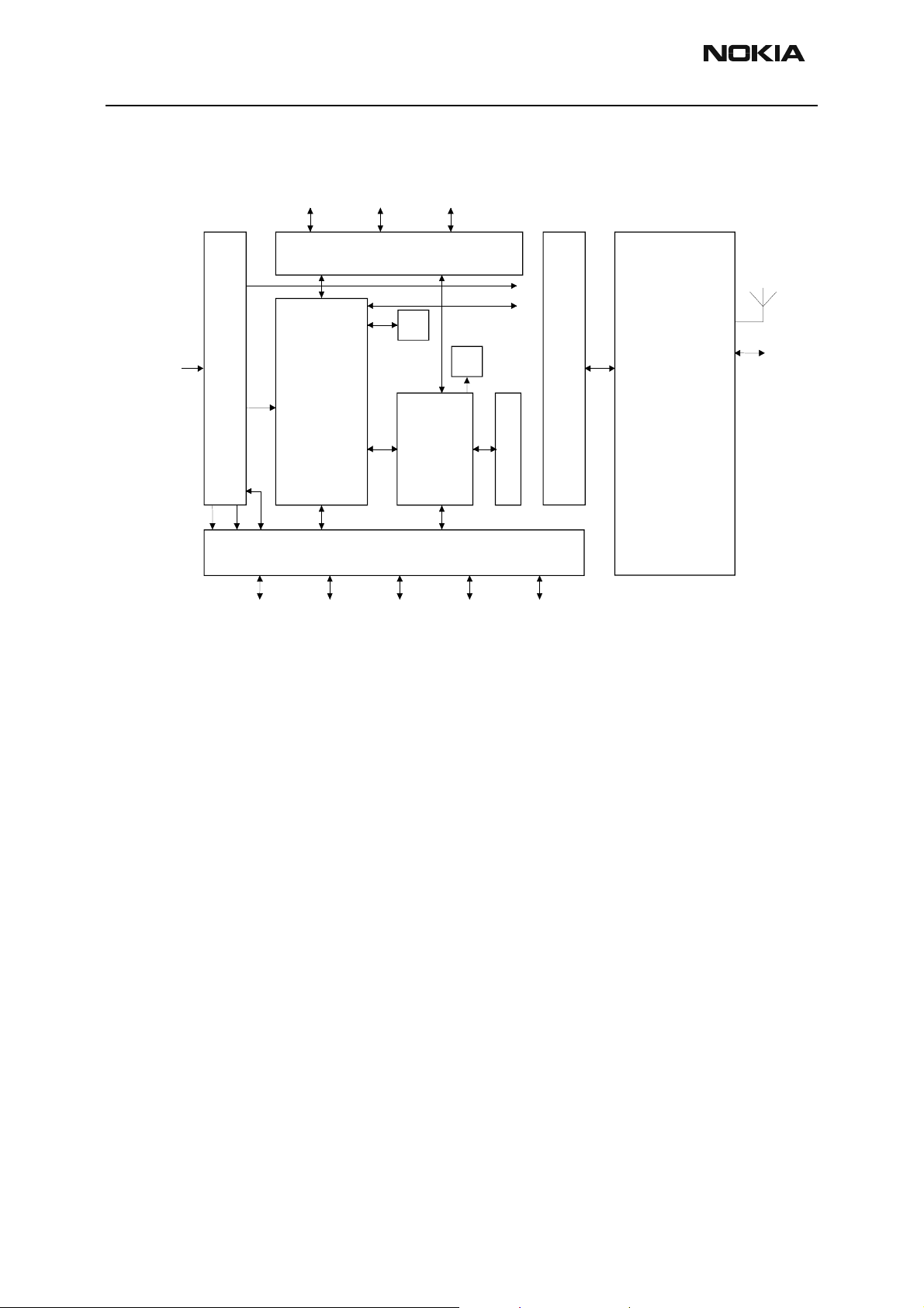
Figure 1: Block diagram of RL7 module
Ostrich
Production
test patte rn
TEST
R&D test
structures
SIM
UI
UEM
UPP
AIF
Internal
RF-
antenna
BB
I
N
T
E
R
F
L
A
S
F
A
C
E
RF
External
antenna
connecto
H
GENIO-
UART
UPP ASIC provides the MCU, DSP, external memory interface and digital control functions. UEM ASIC contains power supply circuitry, charging, audio processing and RF control hardware.
Technical Summary
Baseband is running from power rails 2.8V analog voltage and 1.8V I/O voltage. UPP core
voltage Vcore can be lowered down to 1.0V, 1.3V and 1.5V. UEM includes 6 linear LDO
(low drop-out) regulators for baseband and 7 regulators for R F. It also includes 4 current
sources for biasing purposes and internal usage. UEM also includes SIM interface which
supports 3V SIM cards. TME-3 does not currently support 1.8 V SIMs.
The interface between the baseband and the RF section is handled by a UEM ASIC. The
UEM provides A/D and D/A conversion of the in-phase and quadrature receive and transmit signal paths and also A/D and D/A conversions of received and transmitted audio signals to and from the user interface. The UEM supplies the analog TXC and AFC signals to
RF section according to the UPP DSP digital control.
Data transmission between the UEM and the UPP is implemented using two serial busses, DBUS for DSP and CBUS for MCU. There are also separate signals for PDM coded
audio. Digital speech processing is handled by the DSP inside UPP ASIC. UEM is a dual
voltage circuit, the digital parts are running from the baseband supply 1.8V and the analog parts are running from the analog supply 2.78V. UEM uses also VBAT directly
FBUS
MBUS
NALOG
DIGITAL
UDIO
I/O
Page 8 Nokia Corporation. Issue 4 12/03
Page 9

Company Confidential TME-3
PAMS Technical Documentation Data Module RL7
The baseband supports external microphone inputs and speaker outputs. Input and output signal source selection and gain control is performed by the UEM according to control messages from the UPP. Analog and digital PCM audio are routed to M2M system
connector.
EMC shielding for baseband is implemented using metal lids. On the other side the module is shielded with PWB grounding. Heat generated by the circuitry is conducted out via
the PWB ground planes.
Modes of Ope ration
The TME-3 has three modes of operation:
• RS-232 Mode (M2M system mode)
• Application mode (AT command mode)
• User Control mode
Internally the RL7 module has the following operating modes:
• NO_SUPPLY
• POWER_OFF
•POWER_ON
• RESET
•SLEEP
• PROTECTION
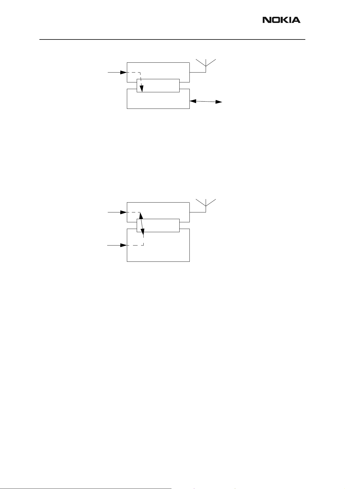
RS232 mode
Fig. 2 shows TME-3 in RS-232 mode. TME-3 enters RS-232 mode in powerup when it
detects a 68k 1% pull-down resistor at M2M system connector pin 21.
In RS-232 mode TME-3 is connected to DAU-12 RS-232 adapter. The adapter provides a
standard RS-232 interface. Power for TME-3 and the adapter is fed through TME-3 DC
jack.
Issue 4 12/03 Nokia Corporation. Page 9
Page 10
TME-3 Company Confidenti al
Data Module RL7 PAMS Techn i cal Documentation
Figure 2: TME-3 RS-232 mode
Voltage input
Application mode
In application mode TME-3 is connected to a user specific application. The mechanical
and electrical interface between application and TME-3 is the M2M system connector.
The application can be powered through M2M system or the application can deliver
power to TME-3.
Voltage input
TME-3
M2M
RS-232 adapter DAU-12
Figure 3: TME-3 in Application mode
TME-3
M2M
RS-232
Alternative voltage
input
User Control mode
In the user control mode the Nokia 30 GSM Connectivity Terminal is controlled by a
mobile phone. Text message templates that are sent from the mob ile to the Nokia 30
instruct the terminal, which in turn controls a device or machine attached to it through
the M2M System connector.
An example of a device attached to the Nokia 30 for wireless control would be a refrigerator. You might want to check the temperature of the refrigerator when out of town.
The temperature of the refrigerator could be altered with the mobile as well.
You could also turn off the lights of the apartment that you had accidentally left on by
sending a text message template.
There are three levels of access control for the User control mode.
Firstly, a message identifier entered when the terminal is used for the first time with the
Nokia 30 Configurator is only known by the person who entered it. This identifier begins
every text message template aimed to control the Nokia 30 and the application attached
to it.
User specific
application
Page 10 Nokia Corporation. Issue 4 12/03
Page 11
Company Confidential TME-3
PAMS Technical Documentation Data Module RL7
Secondly, it can be specified from which phone number the text message templates are
allowed.
Thirdly, a password can be used that is entered whenever a text message template is sent
to the Nokia 30.
Internal operation modes
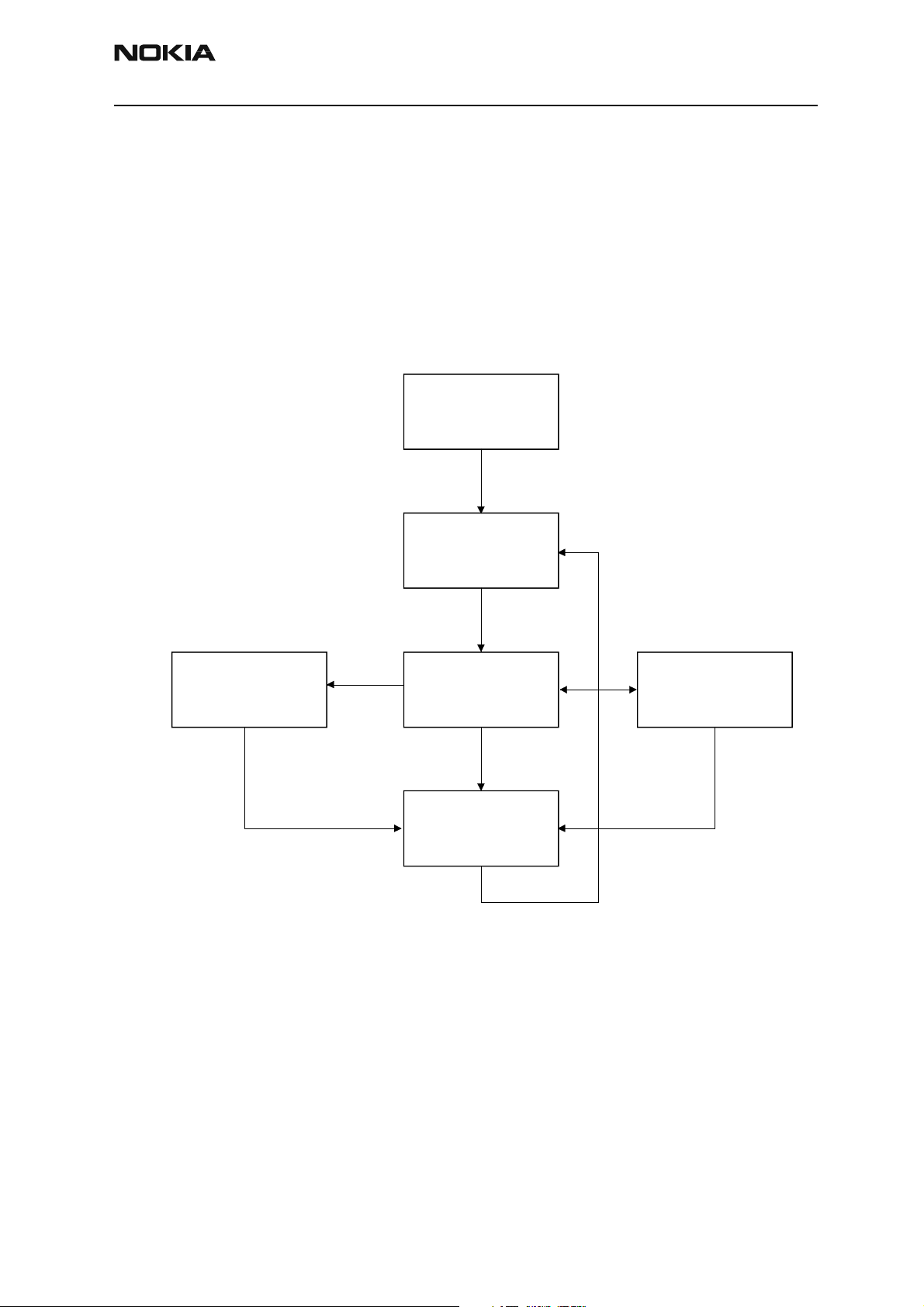
A simplified flow chart of the internal operation modes of TME-3 below.
Figure 4: Internal operation modes
NO_SUPPLY
VBAT
appears
RESET
Thermal
shutdown
POWER_ONPROTECTION SLEEP
Watchdog
bites
Watchdog
bites
POWER_OFF
Always
(forced by HW)
In NO_SUPPLY mode the phone has no supply voltage.
When battery voltage appears, TME-3 enters RESET mode. In TME-3, RESET mode leads
always to POWER_ON mode. During low activity TME-3 can switch f rom POWER_ON to
SLEEP mode. PROTECTION mode happens if the thermal shutdown of UEM regulators
triggers. PROTECTION mode leads immediately to POWER_OFF mode. TME-3 can enter
POWER_OFF mode also from POWER_ON or SLEEP modes if the UEM internal watchdog
elapses. POWER_OFF mode is not stationary.
In TME-3 there is a special power-up hardware, which essentially presses automatically
the power key as soon as it detects the POWER_OFF mode.
Issue 4 12/03 Nokia Corporation. Page 11
Page 12
TME-3 Company Confidenti al
Data Module RL7 PAMS Techn i cal Documentation
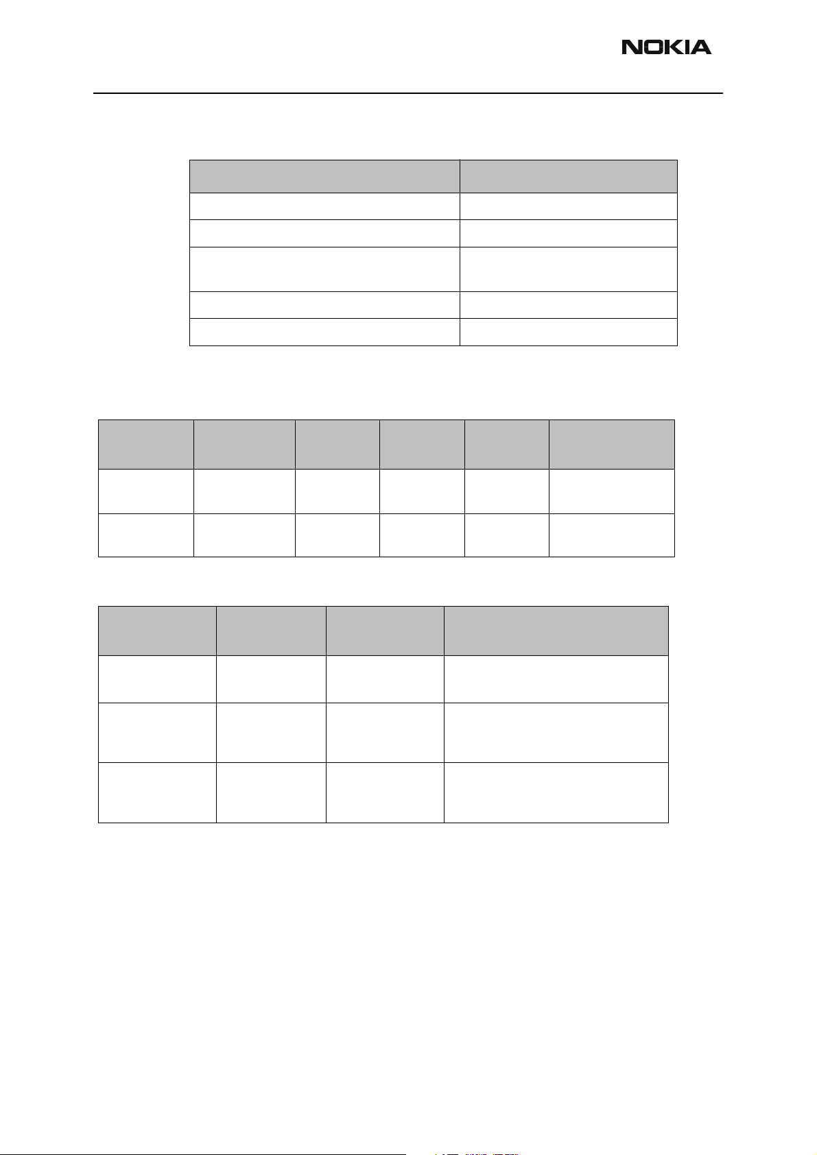
Nominal and maximum ratings
Table 1: s
Parameter Absolute Maximum Rating
Supply voltage maximum VBB 15 V
DC input voltage (any signal pin *) -0.5 to 5.5V*
DC output source or sink current
(any signal pin)
Operating temperature range -10...+55 °C
Storage temperature range -40...+85 °C
+/- 10 mA
DC Characteristics
Table 2: Supply volt a ge
Pin / Conn. Line Symbol Minimum
X100 VBB 6.2 V 12.0 V 14.0 V Power feed through
X101/1,3,5,7,9 VBB 4.75 V 12.0 V 15.0 V Power feed trough
Table 3: Power consumption
Mode
Current / mA @
6.7V
Power / W Notes
Typical /
Nominal
Maximum Notes
DC jack
M2M system
POWER_ON, idle < 10 mA < 120mW
POWER_ON, full
load, 900MHz
POWER_ON, full
load, 1800MHz
< 430 mA < 5.2 W Transmitting 2 slots at full power +
< 350 mA < 4.2 W Transmitting 2 slots at full power +
External signals and connectors
This section describes the external and internal electrical connection and interface levels
on the baseband. The electrical interface specifications are collected into tables that
covers a connector or a defined interface.
External connectors comprise the following:
M2M system., DC, SIM, external antenna.
With one green led on; 65 mW
with all leds off.
300 mA @ 3.6 V power feed to M2M
system
300 mA @ 3.6 V power feed to M2M
system
Page 12 Nokia Corporation. Issue 4 12/03
Page 13

Company Confidential TME-3
PAMS Technical Documentation Data Module RL7
M2M system connector
M2M system connector X101 is described below:
Figure 5: M2M system connector X101
The M2M system connector is 50 pin male connector. Connector connects the TME-3 to
an external applications, for example to the data-adapter. Connection can be made by
female type socket or ribbon cable connector.
Table 4: M2M system connector pinout
Alternate Name Pin Pin Name Alternate
VBB 1 2 GND
VBB 3 4 GND
VBB 5 6 GND
VBB 7 8 GND
VBB 9 10 GND
VCCAM 11 12 Reset
GND 13 14 GENTXD
GENRXD 15 16 GND
RTSAM 17 18 CTSAM
GND 19 20 MBUS
Service 21 22 GND
MIC+ PCMDCLK 23 24 GND
MIC- PCMSCLK 25 26 PCMTX EAR+
GND 27 28 PCMRX EAR-
GND 29 30 FBUSRX
INPUT1 Reserved 31 32 GND
INPUT2 DTR 33 34 FBUSTX
GND 35 36 RTS INPUT3
OUTPUT1 Reserved 37 38 GND
OUTPUT2 DCD 39 40 DSR OUTPUT3
Issue 4 12/03 Nokia Corporation. Page 13
Page 14

TME-3 Company Confidenti al
Data Module RL7 PAMS Techn i cal Documentation
GND 41 42 CTS OUTPUT4
OUTPUT5 RI 43 44 GND
Reserved 45 46 Reserved
GND 47 48 Reserved
Reserved 49 50 GND
in numbering of the M2M system connection
Odd pins are on the left side of the connector, i.e. 1, 3, 5, 7, etc. Even numbers on the
right side of the connector, i.e. 2, 4, 6, 8, etc. Pin 1 is at left top, pin 50 right bottom.
In ribbon cable connection the red stripe conductor of the cable marks pin connection 1.
Conductor numbering is then subsequent from 1 to 50 in the cable
DC connector
DC connector X100, described below, is a 3.2 mm DC jack type connector. VIN is connected to the central pin and the jacket is GND.
Table 5: DC connector pin
Signal Name Pin Notes
GND 3,4
VIN 2 6.2 V – 14.0 V power feed
The connector circuitry composes a 2.0 A fuse and transient protection components.
Power jack tap is a positive (VIN) and border area is a ground (GND).
Page 14 Nokia Corporation. Issue 4 12/03
Page 15

Company Confidential TME-3
PAMS Technical Documentation Data Module RL7
SIM connector
SIM connector X200
cards are not supported.
SIM
C5 C6 C7
C1C2C3
From Battery Type
From SIM Card contact
C8
C4
interface supports both 1.8V and 3V SI M cards. Note t hat 5V SIM
The contacts are described below:
Figure 6: SIM connector X200
GND
UPP
SIMDATA
SIMCLK
SIMRST
VSIM
BSI
SIMCardDet
GND
UEM
SIMIF
register
SIMIO
SIMClk
Data
UEM
digital
logic
SIMIO
SIMClk
Data
UIF Block
UEMInt
CBusDa
CBusEnX
CBusClk
Name Card pin Description
VSIM C1 SIM voltage supply 1.8/3.0V
SIMRST C2 SIM reset
SIMCLK C3 SIM clock
SIMDATA C4 SIM bidirectional data
VPP C5 Unconnected.
GND C7
External antenna connector
External antenna connector X502 interface is used to get better RF sign al in bad
receiving conditions.
Table 6: SIM connector
Figure 7: External antenna connector X502
Issue 4 12/03 Nokia Corporation. Page 15
Page 16

TME-3 Company Confidenti al
Data Module RL7 PAMS Techn i cal Documentation
Functional Description
POWER
TME-3 operates with external DC wall power supply without a battery. The DC voltage
can be supplied either trough the DC jack or the M2M syste m connector. TME-3 has a
wide supply range high efficiency synchronous switched mode step-down converter,
which regulates the input voltage down to normal battery voltage level (3.6V).
Powe r Di st ri b ut i o n
Input voltage from DC connector or M2M system (VBB) is fed to step-down DC-DC converter, which regulates the voltage to 3.6V. The 3.6V is fed to DCT4 power management
circuit UEM (VBAT), to a 3V3 LDO and to the RF power amplifier (VBATRF). UEM regulates
VBAT further for baseband and RF. The 3V3 LDO is used for M2M system I/O buffers.
VBAT is fed to M2M system connector through a switch controlled by UPP.
An application can also draw current directly from the fused input voltage (VBB). The
available current depends on the input voltage and the power consumption of TME-3.
Typical maximum power consumption of TME-3 is less than 5.5 W (including the 300 mA
power feed to the application) in all circumstanc es. For example, if the input voltage is
12.0 V, the application can draw at most 2A - 5.5 W / 12 V = 1540 mA of current without blowing the fuse. However, it is advisable to derate the fuse current to 75% or 1.5 A,
which in the example above leaves ~1000 mA current for the application.
UEM
Figure 8: TME-3 power distribution.
VIN
6.5 V - 8.2 V
DC
Jack
4.75 V - 15.0 V power feed
from AIF
VBB
Power fail
indicator
DC/DC
Step-down
converter
680u
RFC
60R/100M
RFC
60R/100M
To UPP
Power feed/indication
to AIF
3 x 680u
VBAT
3 x 680u
Control
from UPP
VBATRF
LDO
Load switch
3V3
UEM
PA
AIF_3V3
BB
regulators
RF
regulators
300mA power
feed to AIF
AIF
I/O buffers
VCCAM
A
I
F
UEM is an energy management IC. In addition to energy management functionality the
UEM performs all the baseband mixed-signal functions.
User Interface
The TME-3 user interface consist of three two-coloured ( green/red) leds.
Page 16 Nokia Corporation. Issue 4 12/03
Page 17

Company Confidential TME-3
PAMS Technical Documentation Data Module RL7
Six I/O pins from UPP port1, which is normally used for keyboard, are used for led control. Leds are buffered with digital transistors. shows the allocation of led control pins.
Table 7: UI LEDs
BitIO pin # Function Description
P10 LED1 – Green LED Control: 1 = ON, 0 = OFF
P11 LED1 – Red LED Control: 1 = ON, 0 = OFF
P12 LED2 – Green LED Control: 1 = ON, 0 = OFF
P13 LED2 – Red LED Control: 1 = ON, 0 = OFF
P14 LED3 – Green LED Control: 1 = ON, 0 = OFF
P15 LED3 – Red LED Control: 1 = ON, 0 = OFF
The leds are connected between VBAT and ground, and there is a current limiting resistor
and a transistor switch in series with every le d. An 1.8V level active high control signal
from UPP KEYB(10:0) switches the leds on and off. The current through a green led is
~15mA, and the current through a red led is ~5mA. This unsymmetry in led drive currents
ensures that the brightnesses of leds are equal.
UPP Processor
UPP contains ARM7 and LEAD3 MCU & DSP cores, RAM memory and custom logic.
The UPP block contains also an external flash memory. TME-3 flash size is 32Mbit.
M2M system
The M2M system block contains the M2M system connector and the glue logic needed to
make connections between application and the TME-3. The application interface of TME3 is the standard M2M application interfac e. The M2M system interface includes FBUS,
MBUS, GENIOUSART, analog and digital audios (multiplexed to same pins), DC input voltage, regulated 3.6V battery voltage and some general purpose I/Os.
All signal pins of M2M system are 5V tolerant. The 5V input voltage level is translated
down to 2.78V and 1.8V logic levels for UEM and UPP. The outputs of M2M system are
translated from UPP/UEM 1.8V and 2.78V levels to 3.3V level.
M2M system connector is a 50-pin male connector.
SIM
The SIM block contains a SIM card reader, which is connected to UEM SIM interface.
Audio
TME-3 does not have any built-in audio equipment, such as microphone or earpiece.
All audio signals are routed outside of TME-3 via M2M system connector to an external
audio accessory. The RAE-3 does not include or support vibra and buzzer.
Issue 4 12/03 Nokia Corporation. Page 17
Page 18

TME-3 Company Confidenti al
Data Module RL7 PAMS Techn i cal Documentation
The audio control and processing is done by the UEM, which contains the audio codec.
The UPP contains MCU and DSP blocks, handling and processing the audio data signals.
The baseband supports one external microphone input and one external earphone output
or alternatively digital PCM lines.
Audio Interfaces
TME-3 has two different audio types, digital and analog audios. Those lines are multiplexed in M2M system connector, so there is only one physical audio interface.
Figure 9: Audio control diagram
AUDIOSELECT
Audio type selection is made by the audioselect signal from UPP genio pin 28. Audio lines
are multiplexed and demuxed by using NC7SB3157 and these components are controlled
by the audioselect signal
Earpiece electrical interface
Earpiece circuit includes two ferrite beads, two capacitors (27 pF -> 900 MHz cut-off filter) and two varistors for EMC protection. Earphone lines from the M2M system is connected to the differential output (EARP and EARN) in the UEM audio codec.
EARPCMRX
EAR+
PCMTX
AUDIOSELECT
MICPCMSCLK
MIC+
PCMDCLK
AIF 26
AIF 28
MUX 4/2
AIF 23
AIF 25
DEMUX 2/4
Microphone electrical interface
The microphone electrical circuit incl udes EMI/ESD protections which is placed near
the M2M system connector. MICB1 is connected to MIC1P via 1kΩ resistor.
Page 18 Nokia Corporation. Issue 4 12/03
Page 19

Company Confidential TME-3
PAMS Technical Documentation Data Module RL7
RF Module
This RF module executes all RF functions of the module. RF circuitry is located on one
side (B-side) of the PCB.
EMC leakage is prevented by three m etal shields. The first one includes the Bluetooth
module. The second block includes the PA, antenna switch, LNAs and dual RX SAW. The
last block include the Hagar RF IC, VCO, VCTCXO, baluns and balanced filters.
Maximum height inside on RF-shields is 3 mm. Heat generated by t he circuitry will be
conducted out via the PWB ground planes.
Heat generated by the circuitry is conducted out via the PWB ground planes.
Normal and extreme voltages for RF block
There is no extreme voltage due of the internal power block and no battery use.
Parameter Rating
Nominal voltage: 3.6 V (generated in PWR block)
Lower extreme voltage same as nominal
Higher extreme voltage same as nomina l
RF Frequency Plan
Figure 10: RF frequency plan
925-960
MHz
1805-1880
MHz
f
f
f/4
HAGAR
f
f/2f/4
f
f/2
PLL
34203840
MHz
I-signal
I-signalI-signalI-signal
Q-signal
RX
1710-1785
MHz
880-915
MHz
26 MHz
VCTCXO
I-signal
Q-signal
TX
Issue 4 12/03 Nokia Corporation. Page 19
Page 20

TME-3 Company Confidenti al
Data Module RL7 PAMS Techn i cal Documentation
DC characteristics
Regulators
The transceiver comprises a multif unction power management IC on baseband section,
which contains among other functions; 7 pcs of 2.78 V regulators and 4.8V up-switcher
for charge pump.
Use of the regulators can be seen in the Power Distribution Diagram. VrefRF01and
VrefRF02 are used as the reference voltages for HAGAR RF-IC, VrefRF01 (1.35V) for bias
reference and VrfeRF02 (1.35V) for RX ADC's reference.
Regulators (except VR2 and VR7) are connected to HAGAR. Different modes were
switched on by the aid of ser i a l bu s.
List of the supply voltages:
Volt. source Load
VR1 PLL charge pump (4,8 V)
VR2 TX modulator
VR3 VCTCXO + buffer
VR4 HAGAR IC (LNAs+mixer+DTOS)
VR5 HAGAR IC (div+LO-buff+prescaler),
VR6 HAGAR (Vdd_bb)
VR7 VCO
VrefRF01 ref. voltage for HAGAR
VrefRF02 ref. voltage for HAGAR
VbattRF PA
Typical current consumption:
Operation mode Current consumption Notes
Pow er OFF < 10 uA Leakage current (dual PA)
RX 81 mA, peak Includes synthesizer current
(28 mA)
TX, without PA 138 mA, peak
TX, power level 5, EGSM900 1700 mA, peak
TX, power level 0, DCS1800 1200 mA, peak
Page 20 Nokia Corporation. Issue 4 12/03
Page 21

Company Confidential TME-3
PAMS Technical Documentation Data Module RL7
Power Distribution Diagram
SOURCE
VR1
VR2
VR3
VR4
VR5
Figure 11: Power Distribution
4.75 V +/- 3.2 %
10 mA
2.78 V +/- 3 %
100 mA
2.78 V +/- 3 %
20 mA
2.78 V +/- 3 %
50 mA
2.78 V +/- 3 %
50 mA
LOAD
Charge pump in HAGAR
TX IQ modulator, pow er
control opamp in
Hagar
VCTCXO
VCTCXO buffer in Haga r
E-GSM & DCS LNA
RX mixer in Hagar
DTOS in Hagar
PLL in Hagar
UEM
VR6
VR7
VrefRF01
VrefRF02
VBATT
2.78 V +/- 3 %
50 mA
2.78 V +/- 3 %
50 mA
1.35 v +/- 1.15 %
< 100 ua
1.35 V +/- 2 %
< 100 ua
3.2 - 4.5 V
1700 mA (max)
Dividers in Hagar
LO buffers in Hagar
Prescaler in Hagar
Power detector
BB section in Hagar
SHF VCO Module
Ref. volt. for Hagar RX
Ref. volt. for Hagar
Dual PA module
Issue 4 12/03 Nokia Corporation. Page 21
Page 22

TME-3 Company Confidenti al
Data Module RL7 PAMS Techn i cal Documentation
RF characteristics
Main RF characteristics are listed in the table below:
Item Values (E-GSM / GSM1800)
Receive frequency range 925... 960 MHz / 1805...1880 MHz
Transmit frequency range 880... 915 MHz / 1710...1785 MHz
Duplex spacing 45 MHz / 95 MHz
Channel spacing 200 kHz
Number of RF channels 174 / 374
Power class 4 (2 W) / 1 (1 W)
Number of power levels 15 / 16
Transmitter characteristics
Item Values (E-GSM/GSM1800)
Type Direct conversion , nonlinear, FDMA/TDMA
LO frequency range 3520...3660 MHz / 3420...3570 MHz
Output power 2 W / 1 W peak
Gain control range min. 30 dB
Maximum phase error (RMS/peak) max 5 deg./20 deg. peak
Receiver characteristics
Item Values, E-GSM/GSM1800
Type Direct conversion, Linear, FDMA/TDMA
LO frequencies 3700...3840 MHz / 3610...3760 MHz
Typical 3 dB bandwidth +/- 91 kHz
Sensitivity min. - 102 dBm (GSM1800 norm.cond. only)
Total typical receiver voltage gain
(from antenna to RX ADC)
86 dB
Receiver output level (RF level -95 dBm) 230 mVpp, single-ended I/Q signals to RX
ADCs
Typical AGC dynamic range 83 dB
Accurate AGC co ntrol range 60 dB
Usable input dynamic range -102... -10 dBm
RSSI dynamic range -110... -48 dBm
Page 22 Nokia Corporation. Issue 4 12/03
Page 23

Company Confidential TME-3
PAMS Technical Documentation Data Module RL7
RF Block Diagram
26 MHz
RXI
INP_G_RX
INM_G_RX
Balanced
SAW
RXQ
VCP
VPP
VRF_RX
VLO/VPRE
INP_P_RX
INP_P_RX
VB_EXT
VREF_RX
SLE
SCLK
RESET
HAGAR
LNAB_P
LNAB_G
SDATA
LNA_D
LNA_P
VANT_2
VANT_1
LNA_G
Balanced
SAW
TXP
TXC
DET
VTXLO_P
VPCTRL_P
OUTP_P_TX
OUTM_P_TX
GND
TXIM
RF_TEMP
VTX_B_P
VP_D_SEL
TXIP
VTXLO_G
VPCTRL_G
OUTP_G_TX
OUTM_G_TX
TOUT
TXOP
TXOM
VCTCXO
VTX_B_G
VB_DET
VC_1
VC_2
INP_LO
INM_LO
OUT_CP
Balanced
SAW
MMIC
LNA
MMIC
LNA
Dual SAW
Dual PA
module
Dual
coupler
RX/TX switch
3420 - 3840 MHz
Internal
antenna
RF B l oc k Di agram
EGS M900/
GSM1800
Issue 4 12/03 Nokia Corporation. Page 23
Page 24

TME-3 Company Confidenti al
Data Module RL7 PAMS Techn i cal Documentation
Frequency synthesizers
VCO frequency is locked with PLL into stable frequency source, which is a VCTCXO-module. VCTCXO is running at 26 MHz. Temperature drifting is con trolled with AFC voltage.
VCTCXO is locked into frequency of the base station. AFC is generated by baseband with
a 11 bit conventional DAC. 13MHz VCTC XO can also be used if multislot operations is not
needed.
Figure 12: Phase Locked Loop, PLL
26 MHz frequency reference
R
f
ref
f_out /
PHASE
M
DET.
CHARGE
PUMP
AFC-controlled VCTCXO
LP
f_out
VCO
Kd
M
Kvco
M = A(P+1) + (N-A)P=
= NP+A
PLL is located in HAGAR RF-IC and is controlled via serial RFBus. There is 64/65 (P/P+1)
prescaler, N- and A-divider, reference divider, phase detector and charge pump for the
external loop filter. SHF local signal, generated by a VCO-module, is fed through a
180deg balanced phase shifter to prescaler. Output of the prescaler is fed to N- and Adivider, which produces the input to phase detector.
Phase detector compares this signal to reference signal (400kHz), which is divided with
reference divider from VCTCXO output. Output of the phase detector is connected into
charge pump, which charges or discharges integrator capacitor in the loop filter depending on the phase of the measured frequency compared to reference frequency.
Loop filter filters out comparison pulses of phase detector and generates DC control voltage to VCO.
Dividers are controlled via serial bus. RFBus Data is for data, RFBusClk is serial clock for
the bus and RFBusEna1X is a latch enable, which stores new data into dividers.
LO-signal is generated by SHF VCO module. VCO has double frequency in GSM1800 and x
4 frequency in EGSM compared to actual RF channel frequency. LO signal is divided by
two or four in HAGAR (depending on system mode).
Receiver
Receiver is a direct conversion, dual band linear receiver. Received RF-signal from the
antenna is fed via a RF-antenna switch module to the 1st RX bandpass RF-SAW filters
and MMIC LNAs. RF-antenna switch module contains upperband and lowerband opera-
Page 24 Nokia Corporation. Issue 4 12/03
Page 25

Company Confidential TME-3
PAMS Technical Documentation Data Module RL7
tion. The LNA amplified signal is fed to 2nd RX bandpass RF-SAW filters. Both 2nd RX
bandpass RF-SAW filters comprise un-bal/bal configuration to get the balanced (balanced) feed for Hagar.
Discrete LNAs have three gain levels. The first one is max. gain, the second one is about 30dB(GSM1800) and -25dB(EGSM900) below max. gain and the last one is off state. The
gain selection control of LNAs comes from HAGAR IC.
Differential RX signal is amplified and mixed directly down to BB frequency in HAGAR.
Local signal is generated with external VCO. The VCO signal is divided by 2 (GSM1800) or
by 4 (E-GSM900). PLL and dividers are in HAGAR-IC.
From the mixer output to ADC input RX signal is divided into I- and Q-signals. Accurate
phasing is generated in LO dividers. After the mixer DTOS amplifiers convert the differential signals to single ended. DTOS has two gain stages. The first one has constant gain of
12dB and 85kHz cut off frequency. The gain of second stage is controlled wit h contro l
signal g10. If g10 is high (1) the gain is 6dB and if g10 is low (0) the gain of the stage is
-4dB.
The active channel filters in HAGAR provides selectivity for channels (-3dB @ +/-91 kHz
typ.). Integrated base band filter is active-RC-filter with two off-chip capacitors. Baseband filter consists of two stages, DTOS and BIQUAD. DTOS is differential to single-ended
converter having 8dB or 18dB gain. BIQUAD is modified Sallen-Key Biquad.
Integrated resistors and capacitors are tunable. These are controlled with a digital control word. The correct control words that compensate for the process variations of integrated resistors and capacitors and of tolerance of off-chip capacitors are found with the
calibration circuit.
Next stage i n the r eceiv er cha in is a A GC-am plifier, also integrated into HAGAR. AGC has
digital gain control via serial mode bus. AGC-stage provi d es gain control range (40 dB,
10 dB steps) for the receiver and also the necessary DC compensation. Additional 10 dB
AGC step is implemented in DTOS stages.
DC compensation is made during DCN1 and DCN2 operations (controlled via serial bus).
DCN1 is carried out by charging the large external capacitors in AGC stages to a voltage
which cause a zero dc-offset. DCN2 set the signal offset to constant value (VrefRF_02
1.35 V). The VrefRF_02 signal is used as a zero level to RX ADCs.
Single ended filtered I/Q-signal is then fed to ADCs in BB. Input level for ADC is 1.45 Vpp
max.
Transmitter
Transmitter chain consists of two final frequency IQ-modulators fo r upper and lower
band, a dual power amplifier and a power control loop.
I- and Q-signals are generated by baseband. After post filtering (RC-net work) they go
into IQ-modulator in HAGAR. LO-signal for modulator is generated by VCO and is divided
Issue 4 12/03 Nokia Corporation. Page 25
Page 26

TME-3 Company Confidenti al
Data Module RL7 PAMS Techn i cal Documentation
by 2 or by 4 depending on system mode. There are separate outputs one for EGSM and
one for GSM1800.
In EGSM branch there is a SAW filter before PA to attenuate unwanted signals and wideband noise from the Hagar IC.
The final amplification is realized with dual band power amplifier. It has two different
power chains one for EGSM and one for GSM1800. PA is able to produce over 2 W (0
dBm input level) in EGSM band and over 1 W (0 dBm input level) in upperband band into
50 ohm output. Gain control range is over 45 dB to get desired power levels and power
ramping up and down.
Any harmonics generated by the PA are filtered out with filtering in side the antenna
switch -module.
Power control circuitry consists of discrete power detector (common for lower and
upperband) and error amplifier in HAGAR. There is a direction al coupler connected
between PA output and antenna switch. It is a dual band type and has input and outputs
for both systems. Directional coupler takes a sample from the forward going power with
certain ratio. This signal is rectified in a schottky-diode and it produces a DC-signal after
filtering.
The possibility to improve efficiency in low power levels has been specified in power
amplifier module. The improved efficien cy will take place on power level 7 and lower in
EGSM. For this option there is control input line in PA module.
AFC function
AFC is used to lock the transceivers clock to frequency of the base station. AFC-voltage is
generated in BB with 11 bit DA-converter. There is a RC-filter in AFC control line to
reduce the noise from the converter. Settling time requirement for the RC-network
comes from signalling, how often PSW (pure sine wave) slots occur. AFC tracks base station frequency continuously, so transceiver has a stable frequency, because changes in
VCTCXO-output don't occur so fast (temperature).
Settling time requirement comes also from the start up-time allowed. When transceiver
is in sleep mode and "wakes" up to receive mode, there is only about 5 ms for the AFCvoltage to settle. When the first burst comes in system clock has to be settled into +/-
0.1 ppm frequency accuracy. The VCTCXO-module requires also 5 ms to settle into final
frequency. Amplitude rises into full swing in 1... 2 ms, but frequency settling time is
higher so this oscillator must be powered up early enough.
DC-compensation
DC compensation is made during DCN1 and DCN2 operations (controlled via serial bus).
DCN1 is carried out by charging the large external capacitors in AGC stages to a voltage
which cause a zero dc-offset. DCN2 set the signal offset to constant value (RXREF 1.35
V). The RXREF signal is used as a zero level to RX ADCs.
Page 26 Nokia Corporation. Issue 4 12/03
Page 27

Company Confidential TME-3
PAMS Technical Documentation Data Module RL7
Interfaces and Connectors
Antenna
The TME-3 uses an internal or external dual band antenna.
User Interface Features
The TME-3 does not include a display. All UI functions are performed by Leds located in
the A-cover.
*) Application module controllable
Start-up Operation:
Table 8: Start-up Operation:
LED 1 LED 2 Status LED Description
- - - Power off / silent mode
Green scan Green scan Green scan Power on, connecting to network
- Red blink - PIN query / new PIN query
- Red blink Red blink PUK query
Intensity of Field Strength:
Red blink - - Non-acceptable <-105 dBm
Green Blink - - -105 … -100 dBm
Green - - Weak -100 … -95 dBm
Green Green Blink - -95 … -90 dBm
Green Green - Moderate -90 … -85 dBm
Green Green Green Blink -85 … -80 dBm
Green Green Green Good >-80 dBm
Issue 4 12/03 Nokia Corporation. Page 27
Page 28

TME-3 Company Confidenti al
Data Module RL7 PAMS Techn i cal Documentation
Normal Operation:
Table 9: Normal Oper ation:
LED 1 LED 2 Status LED Description
* * Green In service
* * Green blink Call on
* * Green blink Inc o mi n g call
* * Green/Red blink Message received / Voice mail in box
* * Red blink Message arriving and memory is full
*) Application module controllable in M2M System mode
Special Operation:
Table 10: Special Operation:
LED 1 LED 2 Status LED Description
Green/Red blink Green/Red blink Green/Red blink Insert SIM card
Red blink Red blink Red blink Failure, contact service
Yellow Yellow Yellow Initialising
Page 28 Nokia Corporation. Issue 4 12/03
Page 29

Company Confidential TME-3
PAMS Technical Documentation Data Module RL7
Data Module RL7 Parts List
0201802 RL7 RF/Syst Module EDMS Issue: 5.0
Table 11: Parts list RL7_11
Item Code Side Coordinates Part data Part name, t ype
A1 9517089 Top C 7 RF-SHIELD SHIELD_DMC04003
A3 9517138 Top H 8 RF-SHIELD SHIELD_DMC04002
A4 9517137 Bottom N 5 RF-SHIELD 3 SHIELD_DMC04001
A5 9510791 Top I 4 RF-SHIELD 2 SHIELD_DMC04000
A3 9510729 Top H 8 Lid 4 dmd07543
A4 9510728 Bottom N 5 Lid 3 dmd07542
A5 9519722 Top I 1 Lid 2 dmd07511
B200 4510219 Top I 5 32.768KHZ+-30PPM 9PF CRYSTAL_CX_4V
C100 2320805 Bottom J 3 Chipcap X5R 100N K 10V 0402 0402C
C101 2320805 Bottom L 3 Chipcap X5R 100N K 10V 0402 0402C
C10 2 2320805 Bottom H 3 Chipcap X5R 100N K 10V 0402 0402C
C103 2320805 Top E 1 Chipcap X5R 100N K 10V 040 2 0402C
C104 2320805 Top H 1 Chipcap X5R 100N K 10V 040 2 0402C
C105 2320805 Top H 2 Chipcap X5R 100N K 10V 040 2 0402C
C107 2610039 Bottom M 2 CHIPTCAP 68U M 25V 7.3X4.3X4.1 TANT_TPSE
C109 2320783 Top I 4 Chipcap X7R 33N K 10V 0402 0402C
C110 2320783 Top I 4 Chipcap X7R 33N K 10V 0402 0402C
C111 2320744 T op G 2 Chipcap X7R 10% 50V 0402 0402C
C112 2320744 T op G 1 Chipcap X7R 10% 50V 0402 0402C
C113 2320481 Bottom L 3 Chipcap X5R 1U K 6V3 0603 0603C
C114 2312243 Bottom K 2 Chipcap X5R 4U7 K 6V3 0805 0805C
C115 2610043 Bottom E 4 CHIPTCAP 680U R 4V0 7.3X4.3X3.8 TANTAL_D4
C116 2610043 Bottom F 4 CHIPTCAP 680U R 4V0 7.3X4.3X3.8 TANTAL_D4
C117 2610043 Bottom F 5 CHIPTCAP 680U R 4V0 7.3X4.3X3.8 TANTAL_D4
C118 23205 46 Bottom G 3 Chipcap 5% NP0 0402C
C119 23205 46 Bottom H 3 Chipcap 5% NP0 0402C
C120 2320 744 Top O 4 Chipcap X7R 10% 50V 0402 0402C
C121 2320805 Top M 4 Chipcap X5R 100N K 10V 0402 0402C
C123 2610043 Bottom M 6 CHIPTCAP 680U R 4V0 7.3X4.3X3.8 TANTAL_D4
Issue 4 12/03 Nokia Corporation. Page 29
Page 30

TME-3 Company Confidenti al
Data Module RL7 PAMS Techn i cal Documentation
Table 11: Parts list RL7_11
Item Code Side Coordinates Part data Part name, t ype
C124 2610043 Bottom M 8 CHIPTCAP 680U R 4V0 7.3X4.3X3.8 TANTAL_D4
C126 2360001 Top O 4 Chipcap X5R 330N K 10V 0603 0603C
C127 2320568 Bottom N 7 Chipcap 5% X7R 0402C
C128 2320 744 Bottom N 7 Chipcap X7R 10% 50V 0402 0402C
C129 2320 744 Top J 1 Chipcap X7R 10% 50V 0402 0402C
C130 2320 744 Top J 1 Chipcap X7R 10% 50V 0402 0402C
C131 2312243 Top M 5 Chipcap X5R 4U7 K 6V3 0805 0805C
C133 2320568 Top M 1 Chipcap 5% X7R 0402C
C134 2320 744 Top M 1 Chipcap X7R 10% 50V 0402 0402C
C135 2320568 Top J 1 Chipcap 5% X7R 0402C
C136 2320 744 Bottom N 2 Chipcap X7R 10% 50V 0402 0402C
C137 2610039 Bottom O 2 CHIPTCAP 68U M 25V 7.3X4.3X4.1 TANT_TPSE
C138 2320 744 Bottom M 3 Chipcap X7R 10% 50V 0402 0402C
C139 2320568 Bottom I 5 Chipcap 5% X7R 0402C
C200 2320481 Top H 5 Chipcap X5R 1U K 6V3 0603 0603C
C201 2320 778 Top H 5 Chipcap X7R 10% 16V 0402 0402C
C202 2320481 Top H 5 Chipcap X5R 1U K 6V3 0603 0603C
C203 2320481 Top G 5 Chipcap X5R 1U K 6V3 0603 0603C
C204 2320481 Top I 5 Chipcap X5R 1U K 6V3 0603 0603C
C205 2320536 Top I 5 Chipcap 5% NP0 0402C
C206 2320536 Top I 4 Chipcap 5% NP0 0402C
C20 7 2320481 Top I 3 Chipcap X5R 1U K 6V3 0603 0603C
C208 2320481 Top G 5 Chipcap X5R 1U K 6V3 0603 0603C
C209 2320805 Bottom I 5 Chipcap X5R 100N K 10V 0402 0402C
C210 2320481 Bottom I 5 Chipcap X5R 1U K 6V3 0603 0603C
C211 2320805 Top I 4 Chipcap X5R 100N K 1 0V 0402 0402C
C212 2320481 Bottom H 5 Chipcap X5R 1U K 6V3 0603 0603C
C213 2320805 Bottom H 4 Chipcap X5R 100N K 10V 0402 0402C
C214 2320481 Top I 4 Chipcap X5R 1U K 6V3 0603 0603C
C215 2320805 Bottom E 5 Chipcap X5R 100N K 10V 0402 0402C
C216 2320481 Top F 4 Chipcap X5R 1U K 6V3 0603 0603C
C217 2320805 Top G 2 Chipcap X5R 100N K 10V 0402 0402C
Page 30 Nokia Corporation. Issue 4 12/03
Page 31

Company Confidential TME-3
PAMS Technical Documentation Data Module RL7
Table 11: Parts list RL7_11
Item Code Side Coordinates Part data Part name, t ype
C218 2320805 Top H 2 Chipcap X5R 100N K 10V 0402 0402C
C219 2320481 Top G 5 Chipcap X5R 1U K 6V3 0603 0603C
C220 2320481 Top G 5 Chipcap X5R 1U K 6V3 0603 0603C
C221 2320805 Top G 2 Chipcap X5R 100N K 10V 0402 0402C
C222 2320481 Top F 5 Chipcap X5R 1U K 6V3 0603 0603C
C223 2320805 Top G 2 Chipcap X5R 100N K 10V 0402 0402C
C224 2320481 Bottom F 4 Chipcap X5R 1U K 6V3 0603 0603C
C225 2320491 Bottom G 5 Chipcap X7R 220N K 10V 0603 0603C
C226 2320481 Bottom H 6 Chipcap X5R 1U K 6V3 0603 0603C
C227 2320481 Top F 3 Chipcap X5R 1U K 6V3 0603 0603C
C228 2320481 Bottom G 3 Chipcap X5R 1U K 6V3 0603 0603C
C229 2320481 Bottom F 4 Chipcap X5R 1U K 6V3 0603 0603C
C230 2320481 Top F 3 Chipcap X5R 1U K 6V3 0603 0603C
C231 2320481 Bottom G 3 Chipcap X5R 1U K 6V3 0603 0603C
C232 2320 744 Top I 3 Chipcap X7R 10% 50V 0402 0402C
C233 2320 744 Top I 3 Chipcap X7R 10% 50V 0402 0402C
C234 2320 744 Bottom H 3 Chipcap X7R 10% 50V 0402 0402C
C235 2320 744 Top I 3 Chipcap X7R 10% 50V 0402 0402C
C236 2320481 Bottom G 4 Chipcap X5R 1U K 6V3 0603 0603C
C237 2320481 Top F 4 Chipcap X5R 1U K 6V3 0603 0603C
C238 2320481 Bottom H 4 Chipcap X5R 1U K 6V3 0603 0603C
C239 2320481 Top F 5 Chipcap X5R 1U K 6V3 0603 0603C
C240 2320481 Top F 4 Chipcap X5R 1U K 6V3 0603 0603C
C241 2320481 Top F 4 Chipcap X5R 1U K 6V3 0603 0603C
C242 2320481 Bottom G 4 Chipcap X5R 1U K 6V3 0603 0603C
C243 2320481 Bottom G 4 Chipcap X5R 1U K 6V3 0603 0603C
C244 2320481 Top F 3 Chipcap X5R 1U K 6V3 0603 0603C
C246 2320481 Top F 4 Chipcap X5R 1U K 6V3 0603 0603C
C247 2320481 Top H 2 Chipcap X5R 1U K 6V3 0603 0603C
C300 2320805 Top J 3 Chipcap X5R 100N K 10V 0402 0402C
C301 2320805 Top J 4 Chipcap X5R 100N K 10V 0402 0402C
C302 2320805 Top K 5 Chipcap X5R 100N K 1 0V 0402 0402C
Issue 4 12/03 Nokia Corporation. Page 31
Page 32

TME-3 Company Confidenti al
Data Module RL7 PAMS Techn i cal Documentation
Table 11: Parts list RL7_11
Item Code Side Coordinates Part data Part name, t ype
C303 2320805 Top K 5 Chipcap X5R 100N K 1 0V 0402 0402C
C305 2320805 Top K 2 Chipcap X5R 100N K 1 0V 0402 0402C
C320 2320 778 Bottom J 5 Chipcap X7R 10% 16V 0402 0402C
C321 2320 778 Bottom J 4 Chipcap X7R 10% 16V 0402C
C322 2320 778 Top I 5 Chipcap X7R 10% 16V 0402C
C323 2320805 Top H 2 Chipcap X5R 100N K 10V 0402C
C324 2320 779 Bottom L 6 Chipcap X7R 100N K 16V 0603_BLM
C400 2320560 Top F 2 Chipcap 5% NP0 0402C
C401 2320560 Top F 2 Chipcap 5% NP0 0402C
C403 2320560 Top H 7 Chipcap 5% NP0 0402C
C500 2320548 Top C 9 Chipcap 5% NP0 0402 C
C501 2320546 Top D 9 Chipcap 5% NP0 0402C
C502 2320526 Top E 8 Chipcap +-0.25pF NP0 0402C
C503 2320560 Top E 9 Chipcap 5% NP0 0402C
C504 2320805 Top E 9 Chipcap X5R 100N K 10V 0402C
C505 2320560 Top G 9 Chipcap 5% NP0 0402C
C506 2320560 Top G 9 Chipcap 5% NP0 0402C
C50 7 2320778 Top D 9 Chipcap X7R 10% 16V 0402C
C550 2320536 Top C 8 Chipcap 5% NP0 0402 C
C551 2320524 Top D 8 Chipcap +-0.25pF NP0 0402C
C552 2320516 Top E 8 Chipcap +-0.25pF NP0 0402C
C553 2320536 Top E 8 Chipcap 5% NP0 0402C
C554 2320805 Top E 7 Chipcap X5R 100N K 10V 0402C
C555 2320560 Top G 8 Chipcap 5% NP0 0402C
C556 2320560 Top G 8 Chipcap 5% NP0 0402C
C557 2320536 Top D 8 Chipcap 5% NP0 0402C
C600 2320548 Top H 7 Chipcap 5% NP0 0402C
C601 2320554 Top G 8 Chipcap 5% NP0 0402C
C602 2320 778 Top I 7 Chipcap X7R 10% 16V 0402C
C603 2320 778 Top I 8 Chipcap X7R 10% 16V 0402C
C604 2320536 Top I 7 Chipcap 5% NP0 0402C
C605 2320805 Top H 9 Chipcap X5R 100N K 10V 0402C
Page 32 Nokia Corporation. Issue 4 12/03
Page 33

Company Confidential TME-3
PAMS Technical Documentation Data Module RL7
Table 11: Parts list RL7_11
Item Code Side Coordinates Part data Part name, t ype
C60 7 2314001 Top G 9 Chipcap NP0 470P J 6V3 0402C
C608 2320783 Top I 8 Chipcap X7R 33N K 10V 0402C
C609 2320562 Top I 8 Chipcap 5% NP0 0402C
C610 2320562 Top I 8 Chipcap 5% NP0 0402C
C611 2320783 Top I 8 Chipcap X7R 33N K 10V 0402C
C612 2320 778 Top I 9 Chipcap X7R 10% 16V 0402C
C613 2320805 Top H 9 Chipcap X5R 100N K 10V 0402C
C614 2320 778 Top I 8 Chipcap X7R 10% 16V 0402C
C615 2320558 Top H 9 Chipcap 5% NP0 0402C
C616 2320552 Top I 7 Chipcap 5% NP0 0402C
C617 2320552 Top I 7 Chipcap 5% NP0 0402C
C620 2320481 Top I 9 Chipcap X5R 1U K 6V3 0603C
C621 2320481 Top I 9 Chipcap X5R 1U K 6V3 0603C
C622 2320481 Top I 9 Chipcap X5R 1U K 6V3 0603C
C623 2320481 Top H 9 Chipcap X5R 1U K 6V3 0603C
C624 2314001 Top H 9 Chipcap NP0 470P J 6V3 040 2C
C625 2314001 Top H 9 Chipcap NP0 470P J 6V3 040 2C
C626 2314001 Top H 9 Chipcap NP0 470P J 6V3 040 2C
C650 2320554 Top K 7 Chipcap 5% NP0 0402C
C652 2320564 Top J 7 Chipcap 5% NP0 0402C
C653 2322015 Top J 6 Chipcap NP0 2N2 G 16V 0603C
C654 2320564 Top J 6 Chipcap 5% NP0 0402C
C655 2320481 Top K 6 Chipcap X5R 1U K 6V3 0603C
C657 2320520 Top K 7 Chipcap +-0.25pF NP0 0402C
C660 2320560 Top J 8 Chipcap 5% NP0 0402C
C661 2320 779 Top K 8 Chipcap X7R 100N K 16V 0603_BLM
C662 2320536 Top K 8 Chipcap 5% NP0 0402C
C699 2320518 Top F 7 Chipcap +-0.25pF NP0 0402C
C701 2320548 Top F 6 Chipcap 5% NP0 0402C
C70 2 2320548 Top F 7 Chipcap 5% NP0 0402 C
C703 2320554 Top F 7 Chipcap 5% NP0 0402C
C704 2320516 Top C 4 Chipcap +-0.25pF NP0 0402C
Issue 4 12/03 Nokia Corporation. Page 33
Page 34

TME-3 Company Confidenti al
Data Module RL7 PAMS Techn i cal Documentation
Table 11: Parts list RL7_11
Item Code Side Coordinates Part data Part name, t ype
C705 2320548 Top F 7 Chipcap 5% NP0 0402C
C706 2320604 Top F 7 Chipcap 5% NP0 0402C
C707 2320518 Top F 8 Chipcap +-0.25pF NP0 0402C
C709 2312243 Top E 6 Chipcap X5R 4U7 K 6V3 0805C
C710 2320 778 Top B 4 Chipcap X7R 10% 16V 0402 0402C
C711 2320548 Top D 4 Chipcap 5% NP0 0402C
C712 2320778 Top D 4 Chipcap X7R 10% 16V 040 2 0402C
C713 2320540 Top E 6 Chipcap 5% NP0 0402C
C714 2320778 Top D 5 Chipcap X7R 10% 16V 040 2 0402C
C715 2320548 Top B 5 Chipcap 5% NP0 0402C
C716 2320548 Top C 7 Chipcap 5% NP0 0402C
C717 2320536 Top C 8 Chipcap 5% NP0 0402C
C718 2320778 Top C 7 Chipcap X7R 10% 16V 0402C
C719 2320778 Top C 7 Chipcap X7R 10% 16V 0402C
C720 2320 744 Top B 5 Chipcap X7R 10% 50V 0402C
C721 2320536 Top G 9 Chipcap 5% NP0 0402C
C722 2320536 Top G 8 Chipcap 5% NP0 0402C
C723 2320 744 Top G 6 Chipcap X7R 10% 50V 0402C
C724 2320548 Top B 7 Chipcap 5% NP0 0402 C
C726 2320508 Top G 7 Chipcap +-0.25pF NP0 0402C
C727 2320546 Top E 5 Chipcap 5% NP0 0402C
C728 2320 778 Top D 5 Chipcap X7R 10% 16V 0402C
C730 2320560 Top I 7 Chipcap 5% NP0 0402C
C731 2320524 Top E 7 Chipcap +-0.25pF NP0 0402C
C751 2320560 Top G 7 Chipcap 5% NP0 0402C
C752 2322023 Top G 7 Chipcap NP0 2N2 J 16V 0603C
C753 2320538 Top D 8 Chipcap 5% NP0 0402C
C754 2320538 Top D 7 Chipcap 5% NP0 0402C
C756 2320546 Top D 8 Chipcap 5% NP0 0402C
C759 2320546 Top C 7 Chipcap 5% NP0 0402 C
C780 2320548 Top C 9 Chipcap 5% NP0 0402 C
C781 2320548 Top B 9 Chipcap 5% NP0 0402C
Page 34 Nokia Corporation. Issue 4 12/03
Page 35

Company Confidential TME-3
PAMS Technical Documentation Data Module RL7
Table 11: Parts list RL7_11
Item Code Side Coordinates Part data Part name, t ype
D100 4341053 Bottom I 4 6*BUFFER 1.65V 74LVC07A TSSOP_14
D101 4341053 Bottom F 3 6*BUFFER 1.65V 74LVC07A TSSOP_14
D102 4341307 Bottom I 3 74LVC244 8XBUFFER TSSOP_20
D103 4341243 Top E 1 NC7WZ16 2XBUFFER SC7 0-6 SC70_6_FAIR
D104 4341307 Bottom J 3 74LVC244 8XBUFFER TSSOP_20
D105 4341245 Top G 1 1XMUX/DEMUX 2:1 NC7SB3157 SC70_6_FAIR
D106 4341245 Top G 1 1XMUX/DEMUX 2:1 NC7SB3157 SC70_6_FAIR
D107 4341245 Bottom H 2 1XMUX/DEMUX 2:1 NC7SB3157 SC70_6_FAIR
D108 4341245 Bottom G 2 1XMUX/DEMUX 2:1 NC7SB3157 SC70_6_FAIR
D200 4370825 Top H 4 UEMK W-DOG ENA TO21 TFBGA168
D300 4370873 Top K 4 UPP8M V2.6 F751986E C035 uBGA144
D320 4340831 Bottom K 4 FLASH 2MX16 1,8V FBGA40
F100 5119002 Top M 2 Fuse 2A 32V SMD 1206_FUSE
F101 5119002 Top K 1 Fuse 2A 32V SMD 1206_FUSE
G650 4350243 Top J 7 VCO 3420-3840MHZ 2.7V 20MA VCO_GK_601MNA_2
G660 4510261 Top J 9 VCTCXO 26MHZ+-5PPM 2.7V GSM VCTCXO_KT16
L100 3203743 Bottom N 1 FERR.BEAD 0R03 42R/100MHZ 3A 0805_BLM21
L101 3203743 Bottom M 5 FERR.BEAD 0R03 42R/100MHZ 3A 0805_BLM21
L102 3203715 Bottom H 2 FERRITE BEAD 0R35 240R/100M FERRITE_BK1005
L103 3203715 Bottom G 2 FERRITE BEAD 0R35 240R/100M FERRITE_BK1005
L104 3203743 Bottom N 7 FERR.BEAD 0R03 42R/100MHZ 3A 0805_BLM21
L105 3640109 Bottom N 5 CHIP COIL 15U M 2.0A 12.95X9.4X3 COIL_DO3308
L106 3203743 Top N 1 FERR.BEAD 0R03 42R/100MHZ 3A 0805_BLM21
L107 3203743 Top M 1 FERR.BEAD 0R03 42R/100MHZ 3A 0805_BLM21
L108 3203743 Top J 1 FERR.BEAD 0R03 42R/100MHZ 3A 0805_BLM21
L109 3203743 Top J 1 FERR.BEAD 0R03 42R/100MHZ 3A 0805_BLM21
L110 3640475 Bottom O 3 CHOKE 10U M 0R16 1.1A 6.6X4.45 DT1608
L200 3203741 Top F 5 FERRITE BEAD 0R5 600R/100MHZ 0603_BLM
L201 3203741 Top H 5 FERRITE BEAD 0R5 600R/100MHZ 0603_BLM
L202 3203741 Top G 5 FERRITE BEAD 0R5 600R/100MHZ 0 0603_BLM
L203 3203741 Top F 5 FERRITE BEAD 0R5 600R/100MHZ 0 0603_BLM
L204 3203741 Top F 4 FERRITE BEAD 0R5 600R/100MHZ 0603_BLM
Issue 4 12/03 Nokia Corporation. Page 35
Page 36

TME-3 Company Confidenti al
Data Module RL7 PAMS Techn i cal Documentation
Table 11: Parts list RL7_11
Item Code Side Coordinates Part data Part name, t ype
L205 3203741 Top I 2 FERRITE BEAD 0R5 600R/10 0M HZ 0603_BLM
L500 3646091 Top E 9 CHIP COIL 6N8 J Q27/800M 0402 0402L
L501 3646067 Top G 9 CHIP COIL 18N J Q29/800M 0402 0402L
L502 3646091 Top D 9 CHIP COIL 6N8 J Q27/800M 0402 0402L
L503 3646065 Top D 9 CHIP COIL 12N J Q31/800M 0402 0402L
L550 3646053 Top E 8 CHIP COIL 4N7 +-0N3 Q28/800M 0402L
L551 3646091 Top G 8 CHIP COIL 6N8 J Q27/800M 0402 0402L
L552 3646047 Top D 8 CHIP COIL 3N3 +-0N3 Q28/800M 0402L
L700 3646053 Top G 7 CHIP COIL 4N7 +-0N3 Q28/800M 0402L
L701 3646053 Top G 6 CHIP COIL 4N7 +-0N3 Q28/800M 0402L
L702 3646051 Top G 7 CHIP COIL 3N9 +-0N3 Q28/800M 0402L
L703 3203743 Top E 5 FERR.BEAD 0R03 42R/100MHZ 3A 0805_BLM21
L704 3203715 Top B 4 FERRITE BEAD 0R35 240R/100M FERRITE_BK1005
L705 3646059 Top B 4 CHIP COIL 5N6 +-0N3 Q28/800M 0402L
L708 3645065 Top B 6 CHIP COIL 5N6 K Q98/1.5GHZ 0805 0805HQ
L750 4551015 Top C 7 DIR.COUP 897.5/1747.5/1880MHZ COUPLER_LDC15D
N100 4340663 Bottom L 2 LP2985 REG 3.3V 150A SOT23-5 SOT23_5_H1.45
N101 4341217 Top N 4 DC/DC CONTROL (MAX1653) QSOP16_H1.73
N10 2 434 1215 Bottom J 5 1XCOMP VREF=1.245 MAX9 1 8 SOT23_5_H1.45
N600 4370 781 Top H 8 HAGAR 5 LFBGA80 uBGA80_H1.7
N700 4350 297 Top C 6 PW AMP RF9203E10.1 900/1800
3.5V
R100 1430770 Bottom H 4 Resistor 5% 63mW 0402R
R101 1430770 Bottom H 4 Resistor 5% 63mW 0402R
R10 2 1430770 Bottom H 4 Resistor 5% 63mW 0402R
E5_H1.65
R103 1430770 Bottom I 5 Resistor 5% 63mW 0402R
R104 1430770 Bottom J 4 Resistor 5% 63mW 0402R
R105 1430770 Bottom J 4 Resistor 5% 63mW 0402R
R106 1430770 Bottom G 3 Resistor 5% 63mW 0402R
R107 1430770 Bottom G 3 Resistor 5% 63mW 0402R
R108 1430770 Bottom E 2 Resistor 5% 63mW 0402R
R109 1430770 Bottom G 2 Resistor 5% 63mW 0402R
Page 36 Nokia Corporation. Issue 4 12/03
Page 37

Company Confidential TME-3
PAMS Technical Documentation Data Module RL7
Table 11: Parts list RL7_11
Item Code Side Coordinates Part data Part name, t ype
R110 1430726 Bottom A 4 Resistor 5% 63mW 0402R
R111 1430740 Bottom A 4 Resistor 5% 63mW 0402R
R112 1430726 Bottom C 4 Resistor 5% 63mW 0402R
R113 1430740 Bottom C 4 Resistor 5% 63mW 0402R
R114 1430726 Bottom B 4 Resistor 5% 63mW 0402R
R115 1430740 Bottom B 4 Resistor 5% 63mW 0402R
R116 1430754 Bottom E 3 Resistor 5% 63mW 0402R
R117 1430770 Bottom J 5 Resistor 5% 63mW 0402R
R118 1430873 Bottom I 5 CHIPRES 0W06 27K F 0402 0402R
R119 1430907 Bottom I 5 CHIPRES 0W06 11K F 0402 0402R
R125 1430 762 Top G 2 Resistor 5% 63mW 0402R
R129 1430 762 Top G 1 Resistor 5% 63mW 0402R
R131 1430 714 Bottom G 3 Resistor 5% 63mW 0402R
R132 1430714 Bottom G 3 Resistor 5% 63mW 0402R
R134 1414655 Bottom N 7 CHIPRES 0W125 0R10 J 0805 0805R
R135 1430796 Bottom E 2 Resistor 5% 63mW 0402R
R137 1414655 Bottom O 7 CHIPRES 0W125 0R10 J 0805 0805R
R141 1430804 Top K 2 Resistor 5% 63mW 0402R
R142 1430 796 Top K 2 Resistor 5% 63mW 0402R
R143 1430 770 Top J 1 Resistor 5% 63mW 0402R
R144 1430121 Top N 5 Chipres 0W06 22k F 200ppm 0402 0402R
R145 1430187 Top N 5 Chipres 0W06 47k F 200ppm 0402 0402R
R146 1825005 Bottom N 1 CHIP VARISTOR VWM14V VC30V 0805_VARISTOR_SIOV
R147 1825033 Bottom H 2 CHIP VARISTOR VW14V VC46V 0402 0402_VAR
R148 1825033 Bottom G 2 CHIP VARISTOR VW14V VC46V 0402 0402_VAR
R149 1430 778 Top E 2 Resistor 5% 63mW 0402R
R150 1430 796 Top O 5 Resistor 5% 63mW 0402R
R151 1430690 Top J 2 Chipres 0W06 jumper 0402 0402R
R153 1430 770 Top I 3 Resistor 5% 63mW 0402R
R154 1430 796 Top I 3 Resistor 5% 63mW 0402R
R155 1430770 Bottom K 3 Resistor 5% 63mW 0402R
R156 1430911 T o p I 2 Resistor 1% 63mW 0402R
Issue 4 12/03 Nokia Corporation. Page 37
Page 38

TME-3 Company Confidenti al
Data Module RL7 PAMS Techn i cal Documentation
Table 11: Parts list RL7_11
Item Code Side Coordinates Part data Part name, t ype
R157 1430911 T o p I 2 Resistor 1% 63mW 0402R
R158 1430911 T o p J 3 Resistor 1% 63mW 0402R
R159 1430911 T o p I 2 Resistor 1% 63mW 0402R
R160 1430911 T o p I 3 Resistor 1% 63mW 0402R
R161 1430911 T o p I 3 Resistor 1% 63mW 0402R
R162 1430726 Bottom H 2 Resistor 5% 63mW 0402R
R163 1430726 Bottom G 2 Resistor 5% 63mW 0402R
R164 1430690 Top O 4 Chipres 0W06 jumper 0402 0402R
R202 1620067 Top I 3 RES NETWORK 0W06 4X100K J MNR0804
R204 1430215 Top J 3 CHIPRES 0W06 68K F 200PPM 0402R
R205 1430790 Bottom G 3 Resistor 5% 63mW 0402R
R206 4120071 Bottom A 6 ASIP EMIF03-SIM01 SIM FILTER uBGA8
R20 7 1430778 Bottom H 6 Resistor 5% 63mW 0402R
R320 1430770 Bottom L 6 Resistor 5% 63mW 0402R
R400 1430 778 Top F 2 Resistor 5% 63mW 0402R
R401 1430 778 Top F 2 Resistor 5% 63mW 0402R
R403 1430 726 Top H 7 Resistor 5% 63mW 0402R
R500 1430 726 Top E 9 Resistor 5% 63mW 0402R
R501 1430 700 Top E 9 Resistor 5% 63mW 0402R
R502 1430832 Top D 9 Resistor 5% 63mW 0402R
R520 1430830 Bottom D 2 Resistor 5% 63mW 0402R
R551 1430 700 Top E 7 Resistor 5% 63mW 0402R
R558 1430832 Top D 8 Resistor 5% 63mW 0402R
R600 1620081 Top I 9 RES NETWORK 0W03 4X22R J 0804 MNR04
R602 1430 770 Top I 9 Resistor 5% 63mW 0402R
R603 1430846 Top G 8 Resistor 1% 63mW 0402R
R604 1430 770 Top H 9 Resistor 5% 63mW 0402R
R606 1430 784 Top H 9 Resistor 5% 63mW 0402R
R60 7 1620033 Top I 7 RES NETWORK 0W06 2X5K6 J 0404 0404_R
R608 1620033 Top I 7 RES NETWORK 0W06 2X5K6 J 0404 0404_R
R610 1430 700 Top I 7 Resistor 5% 63mW 0402R
R650 1430137 Top J 6 CHIPRES 0W06 1K0 F 200PPM 0402 0402R
Page 38 Nokia Corporation. Issue 4 12/03
Page 39

Company Confidential TME-3
PAMS Technical Documentation Data Module RL7
Table 11: Parts list RL7_11
Item Code Side Coordinates Part data Part name, t ype
R651 1430907 Top J 6 CHIPRES 0W06 11K F 0402 0402R
R652 1430 700 Top K 7 Resistor 5% 63mW 0402R
R660 1430 762 Top J 8 Resistor 5% 63mW 0402R
R661 1430 774 Top K 8 Resistor 5% 63mW 0402R
R700 1620121 Top G 7 RES NETWORK 0W06 2X220R J MNR02_SR 0404
R701 1620121 Top F 7 RES NETWORK 0W06 2X220R J MNR02_SR 0404
R703 1430 714 Top D 7 Resistor 5% 63mW 0402R
R704 1430 718 Top C 7 Resistor 5% 63mW 0402R
R705 1620515 Top C 4 RES NETWORK 0W04 1DB ATT 0404_RAC10
R706 1430693 Top G 6 Chipres 0W06 5R6 J 0402 0402R
R707 1430693 Top G 7 Chipres 0W06 5R6 J 0402 0402R
R709 1430 734 Top B 7 Resistor 5% 63mW 0402R
R751 1430 770 Top D 7 Resistor 5% 63mW 0402R
R752 1430 788 Top H 7 Resistor 5% 63mW 0402R
R753 1430 770 Top D 8 Resistor 5% 63mW 0402R
R754 1430 726 Top D 7 Resistor 5% 63mW 0402R
R755 1430 718 Top C 8 Resistor 5% 63mW 0402R
R756 1430 770 Top H 6 Resistor 5% 63mW 0402R
R757 1430 778 Top D 7 Resistor 5% 63mW 0402R
R780 1430 700 Top B 9 Resistor 5% 63mW 0402R
R781 1430 700 Top B 9 Resistor 5% 63mW 0402R
T650 3640423 Top I 8 BALUN TRANS 3.7GHZ+/-300MHZ TRANS_LDB15 0805
T700 4550137 Top F 7 TRANSF BALUN 1.8GHZ+-100MHZ TRANS_LDB15 2x1.3
V100 4864511 Top A 7 LED MUW GRN/RED 570/620NM LED_SML_521
V101 4864511 Top A 5 LED MUW GRN/RED 570/620NM LED_SML_521
V102 4864511 Top A 4 LED MUW GRN/RED 570/620NM LED_SML_521
V103 4210043 Bottom B 4 TR DTC143ZE RB=4K7 RBE=47K EM3
V104 4210043 Bottom C 4 TR DTC143ZE RB=4K7 RBE=47K EM3
V105 4210043 Bottom C 4 TR DTC143ZE RB=4K7 RBE=47K EM3
V106 4210043 Bottom A 4 TR DTC143ZE RB=4K7 RBE=47K EM3
V107 4210043 Bottom B 4 TR DTC143ZE RB=4K7 RBE=47K EM3
V108 4210043 Bottom A 4 TR DTC143ZE RB=4K7 RBE=47K EM3
Issue 4 12/03 Nokia Corporation. Page 39
Page 40

TME-3 Company Confidenti al
Data Module RL7 PAMS Techn i cal Documentation
Table 11: Parts list RL7_11
Item Code Side Coordinates Pa rt data Part name, type
V109 4110074 Bottom O 1 SCH DI 40V 3A SOD6
V110 411007 8 Top M 4 S LHDIx 2 70mA SOT323
V111 4211321 Bottom M 3 MFET FDS6912A N 30V 6A 0R035 SO8N2
V112 4211391 Top K 1 MFET P FDC6323L SWITCH 3-8V TSOP_6
V114 4110074 Bottom M 5 SCH DI 40V 3A SOD6
V115 4110078 Top E 2 SLHDIx2 70mA SOT323
V120 4110078 Bottom K 3 SLHDIx2 70mA SOT323
V200 4219926 Bottom I 5 TR+RX2 RN1302 N 50V 50MA 10K SOT323
V201 4219926 Bottom H 5 TR+RX2 RN1302 N 50V 50MA 10K SOT323
V500 4210277 Top D 9 TR BGB420 MIRROR ADJ BIAS SOT343_R
V550 421026 1 Top D 8 TR BGA428 LNA1.8GHZ 19.5DB SOT_363
V750 4110079 Top D 7 SCH DIX2 HSMS282C 15V <1PF SOT323
X100 5409003 Top N 2 SMD JACK 3.0MM F DC 9V 1A SMK_JACK_SWITCH
X101 5400225 Bottom H 1 SM PIN HEADER 2X25M P1.27MM
STR
X200 5409201 Bottom C 6 SM SIM CONN 2X3POL SK51002_001
X502 5429017 Bottom C 3 SM CONN RF PLUG+SW 3GHZ 1W
90DEG
Z100 4120051 Top I 1 EMI ESD FILT10CH IP4026CX25 uBGA_25_P0.75
Z101 4120051 Top F 1 EMI ESD FILT10CH IP4026CX25 uBGA_25_P0.75
Z500 4512133 Top B 8 ANT.SWIT.880-960/1710-1990MHZ 7x5 UM_0318C1
Z501 4511235 Top F 9 SAW FILT 942.5+-17.5MHZ/3.8DB 3x3 DCC6D_H1.15
Z520 4511181 Top D 9 Filter SAW 925-960/1805-1880
MHZ
Z551 4511241 Top F 8 SAW FILT 1842.5+-37.5MHZ/3.5DB 3x3 DCC6D_H1.15
Z700 4511237 Top F 7 SAW FILT 897.5+-17.5MHZ/4.2DB 3x3 DCC6D_H1.15
SAMTEC_ASP_67923_0
2
SWITCH_SHALTER
QCC8B_4.0X4.0
Page 40 Nokia Corporation. Issue 4 12/03
 Loading...