

Page 1

Programmes After Market Services
TME-3 Series Transceivers
Disassembly and T roubleshooting
Issue 3 10/03 Nokia Corporation.
Page 2

TME-3
Disassembly and Troubleshooting PAMS Technical Documentation
[This page intentionally blank]
Page 2 Nokia Corporation. Issue 3 10/03
Page 3

TME-3
PAMS Technical Documentation Disassembly and Troubleshooting
Table of Contents
Page No
Introduction to troubleshooting...................................................................................... 5
Disassembly of TME-3.................................................................................................. 6
RF Troubleshooting ....................................................................................................... 9
Introduction to RF troubleshooting .............................................................................9
Component notes:...................................................................................................... 9
Component handling:................................................................................................ 9
Measurement notes:................................................................................................... 9
RF Key component placement ...................................................................................10
RF Measurement points .............................................................................................11
GSM900 & GSM1800 Transmitter ...........................................................................12
General instructions for Transmitter (Tx) troubleshooting..................................... 12
Transmitter troubleshooting diagrams ..................................................................14
Oscilloscope screen shots of transmitter signals..................................................... 17
GSM900 & GSM1800 Receiver ................................................................................20
General instructions for Rx troubleshooting........................................................... 20
LNA gainstep checking GSM900 & GSM1800 ...................................................24
Synthesizer .................................................................................................................25
General instructions for synthesizer troubleshooting.............................................. 25
Pictures of synthesizer signals................................................................................. 27
Baseband Troubleshooting........................................................................................... 30
Troubleshooting steps ................................................................................................30
Terminal is dead (1) ...................................................................................................31
Terminal is dead (2) ...................................................................................................32
Flashing fault (1) ........................................................................................................33
Flashing fault (2) ........................................................................................................34
Terminal jammed (1) .................................................................................................35
Terminal jammed (2) .................................................................................................36
SIM card fault ............................................................................................................37
Signal diagrams .........................................................................................................38
13 MHz clock.......................................................................................................... 38
26 MHz signal......................................................................................................... 38
Sleep clock signal.................................................................................................... 39
1 MHZ Cbus clock signal........................................................................................ 39
Timing diagram .........................................................................................................40
Flash 1 signal........................................................................................................... 41
Flash 2 signal........................................................................................................... 42
Flash 3 signal........................................................................................................... 42
Issue 3 10/03 Nokia Corporation. Page 3
Page 4

TME-3
Disassembly and Troubleshooting PAMS Technical Documentation
Table of Figures
Page No
Fig 1 SIM card cover removal .............................................................................................6
Fig 2 Screw removal............................................................................................................6
Fig 3 Remove the B-cover...................................................................................................7
Fig 4 B-cover removed ........................................................................................................8
Fig 5 RL7 module component placement 1.........................................................................10
Fig 6 Measurement points, PA 1/2 ......................................................................................11
Fig 7 Measurement points, PA 2/2 ......................................................................................11
Fig 8 Tx troubleshooting......................................................................................................14
Fig 9 Hagar Troubleshooting diagram.................................................................................15
Fig 10 PA&Ant troubleshooting diagram............................................................................16
Fig 11 TXI_0, Tx on, Random data, Burst mode................................................................17
Fig 12 TXQ_0, Tx on, Random data, Burst mode...............................................................17
Fig 13 900/1800 antsw tx contr, Tx on, burst mode............................................................18
Fig 14 900/1800 PA bias, Tx on, burst mode......................................................................18
Fig 15 900/1800 PA ctrl, Tx on, burst mode, high power level ..........................................19
Fig 16 Tx out signal, 900 band, burst mode, channel 37.....................................................19
Fig 17 Receiver signal .........................................................................................................21
Fig 18 Troubleshooting diagram for GSM900 receiver ......................................................22
Fig 19 Troubleshooting diagram for GSM1800 receiver ....................................................23
Fig 20 Synthesizer troubleshooting diagram.......................................................................26
Fig 21 26MHz XO out.........................................................................................................27
Fig 22 13 MHz clock ...........................................................................................................27
Fig 23 4GHz VCO ctrl.........................................................................................................28
Fig 24 4GHz VCO ctrl ........................................................................................................28
Fig 25 4GHz VCO output, 1800 band, RX on, continuous mode.......................................29
Fig 26 Dead terminal, 1 ......................................................................................................31
Fig 27 Dead terminal ...........................................................................................................32
Fig 28 Flashing fault 1.........................................................................................................33
Fig 29 Flashing fault 2 ........................................................................................................34
Fig 30 Terminal jammed (1)................................................................................................35
Fig 31 Terminal jammed (2)................................................................................................36
Fig 32 SIM card fault ..........................................................................................................37
Fig 33 13 MHz clock ...........................................................................................................38
Fig 34 26 MHz signal ..........................................................................................................38
Fig 35 Sleep clock signal.....................................................................................................39
Fig 36 1 MHZ Cbus clock signal.........................................................................................39
Fig 37 Timing diagram ........................................................................................................40
Fig 38 Flash 1 signal............................................................................................................41
Fig 39 Flash 2 signal............................................................................................................42
Fig 40 Flash 3 signal............................................................................................................42
Page 4 Nokia Corporation. Issue 3 10/03
Page 5

TME-3
PAMS Technical Documentation Disassembly and Troubleshooting
Introduction to troubleshooting
The first thing to do is carry out a through visual check of the module. Ensure in particular that:
a) there are not any mechanical damages
b) soldered joints are OK
Issue 3 10/03 Nokia Corporation. Page 5
Page 6
TME-3
Disassembly and Troubleshooting PAMS Technical Documentation
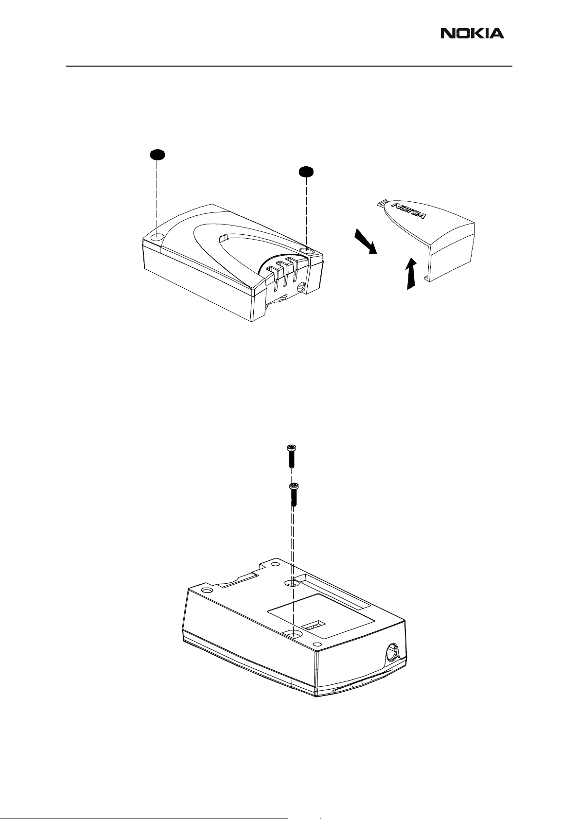
Disassembly of TME-3
1. Remove the lens.
Figure 1: Lens removal
2
1
2. Turn the device upside down and remove the two screws.
Figure 2: Screw removal l
Page 6 Nokia Corporation. Issue 3 10/03
Page 7
TME-3
PAMS Technical Documentation Disassembly and Troubleshooting
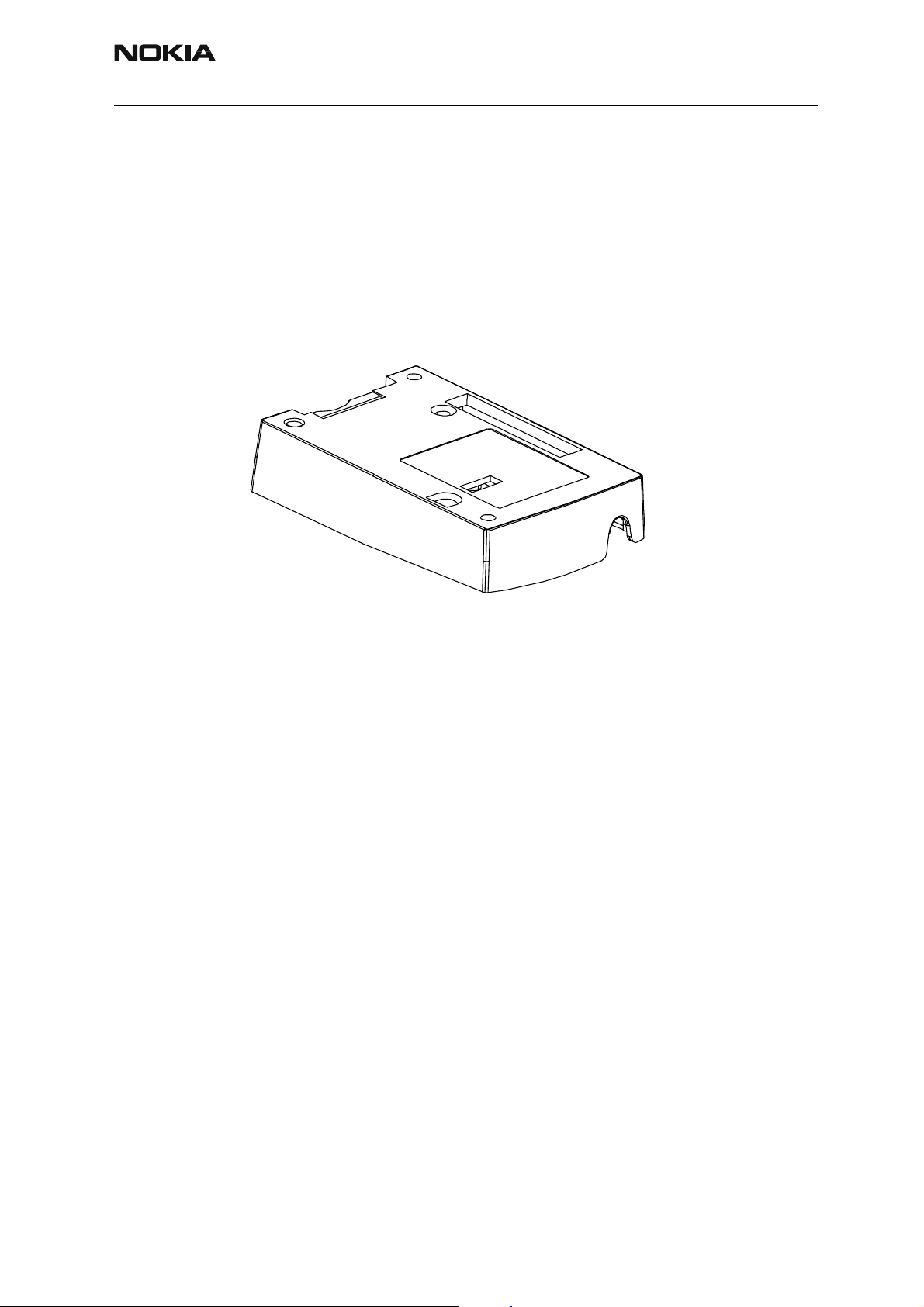
3. Remove the B cover.
Figure 3: Remove the B-cover.
Issue 3 10/03 Nokia Corporation. Page 7
Page 8
TME-3
Disassembly and Troubleshooting PAMS Technical Documentation
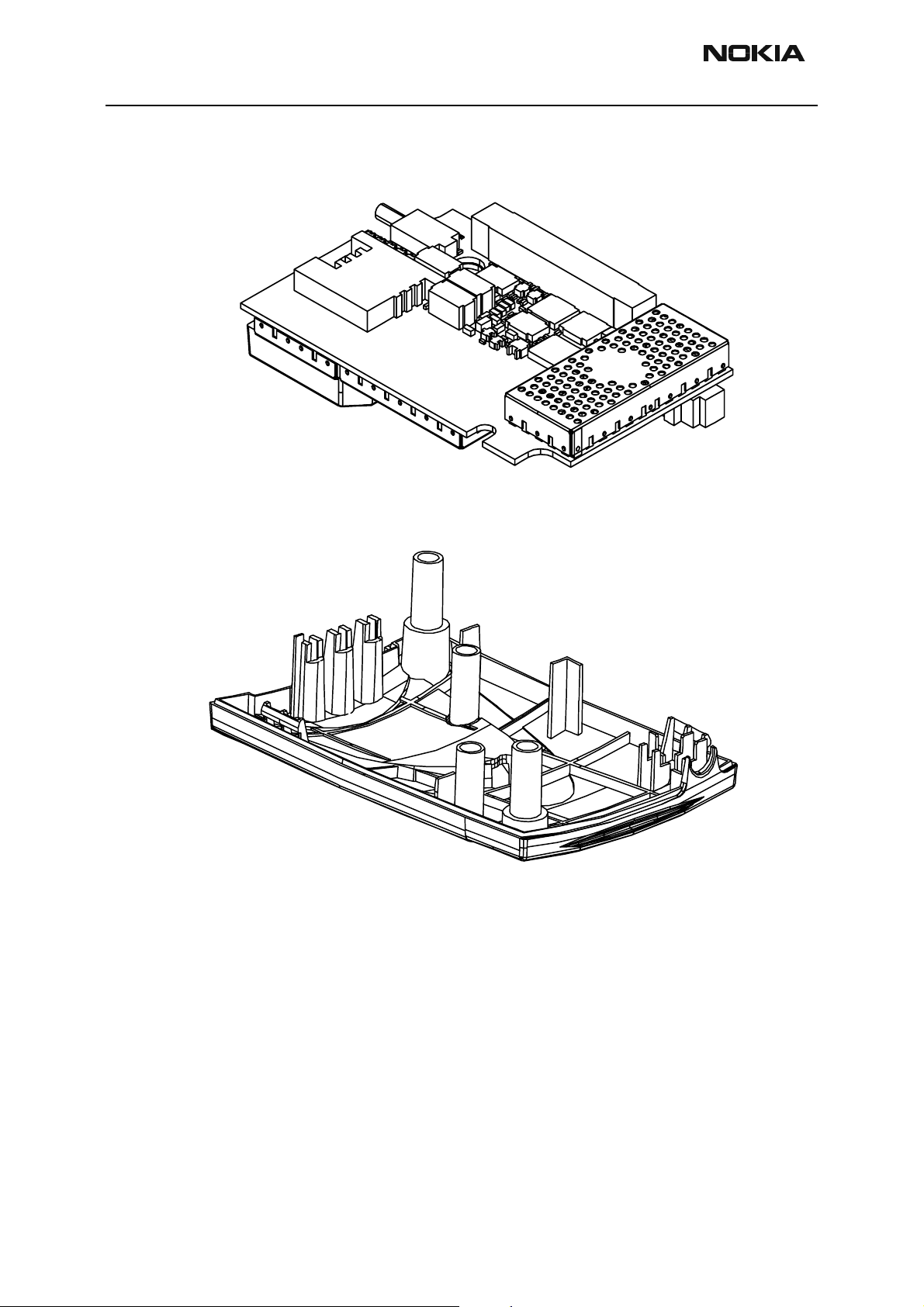
4. Remove the data module from the A-cover
Figure 4: B-cover removed
NOTE: The screws require Torx6 screwdriver tip. Thecorrect tightening torque is 25Ncm.
Page 8 Nokia Corporation. Issue 3 10/03
Page 9

TME-3
PAMS Technical Documentation Disassembly and Troubleshooting
RF Troubleshooting
Introduction to RF troubleshooting
The RF-section of the RL7 module is build around one RF-ASIC (HAGAR, N600). For easier
troubleshooting, the instructions are divided into three sections: transmitter, receiver
and synthesizer.
Component notes:
Apart from key components described in this document here are several discrete components (resistors, inductors and capacitors), the troubleshooting of which is done by
checking whether the soldering of each component is OK.
Capacitors can be checked for short cir cuits and resistors for value by means of an ohmmeter, but be aware that in-circuit measurements must be evaluated carefully.
Before replacing HAGAR, please check following: are the supply voltages and serial communication signals (coming from baseband to HAGAR) correct?
Please note that the grounding of the PA module is directly below the PA-module so it is
difficult to check or change.
Component handling:
Most RF semiconductors are static discharge sensitive! ESD protection must be taken
care of during repair (use ground straps and ESD soldering irons).
HAGAR and PA are moisture sensitive components; parts must be pre-baked prior to sol-
dering.
Measurement notes:
Measurements must be done using spectrum analyzer with high-frequency high-impedance passive probe (LO-/reference frequencies and RF power levels) and oscilloscope
with a 10:1 probe (DC-voltages and low frequency signals)
Please be aware that all measured voltages or RF levels in this document are rough figures. Especially RF levels vary due to different measuring equipment or different grounding of the used probe. When using RF probe usually a good way is to use metallic
tweezers to connect probe ground to PWB ground as close to measurement point as possible.
Issue 3 10/03 Nokia Corporation. Page 9
Page 10
TME-3
Disassembly and Troubleshooting PAMS Technical Documentation
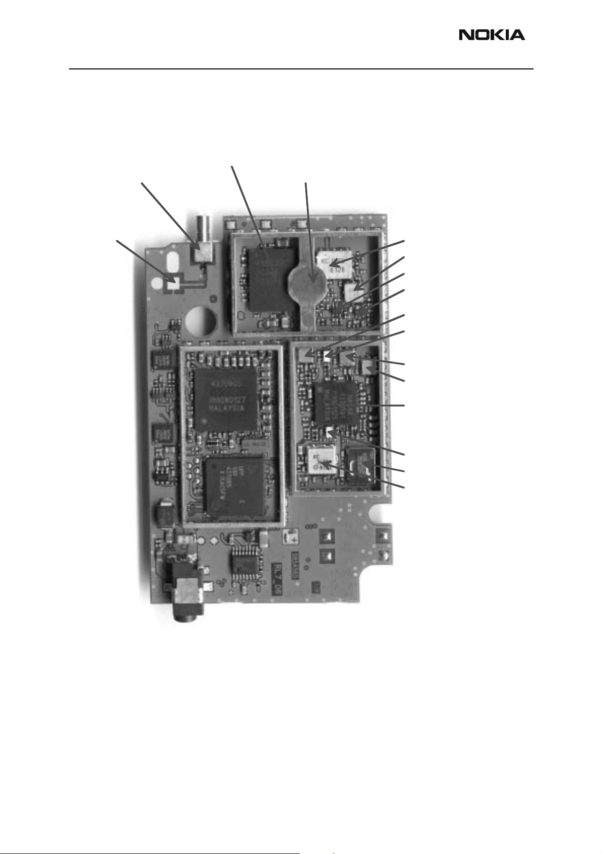
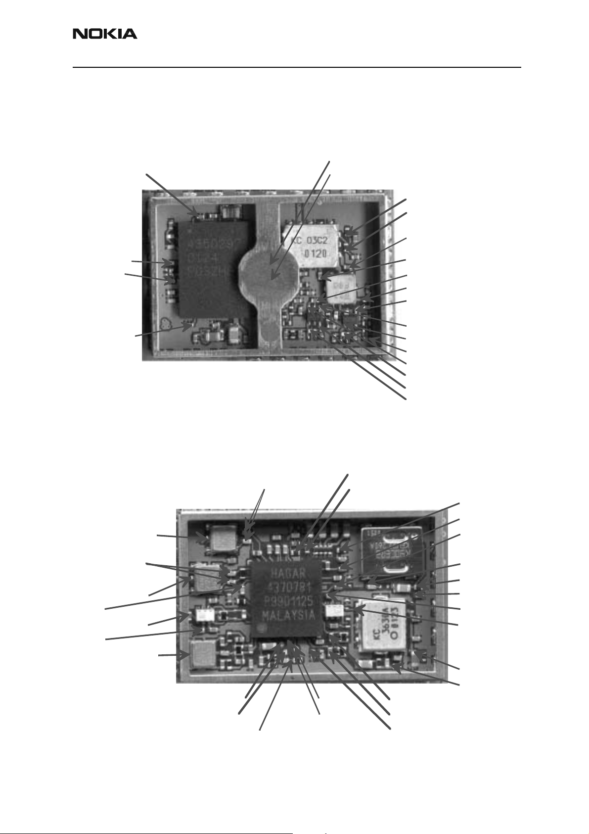
RF Key component placement
Figure 5: RL7 module component placement 1
External antenna
connector/switch
Internal antenna
pad
Dual PA Dual coupler
(under frame)
Antenna switch
Dual RX 1st SAW
PCN LNA
EGSM LNA
EGSM TX SAW
PCN TX balun
PCN RX 2nd SAW
EGSM RX 2nd SAW
HAGAR RFIC
VCO balun
26MHz VCTCXO
4GHz VCO
NOTE! You can remove (cut) the frame above the power amplifier, ex. PA exchange
Page 10 Nokia Corporation. Issue 3 10/03
Page 11
TME-3
PAMS Technical Documentation Disassembly and Troubleshooting
RF Measurement points
PA environment
Figure 6: Measurement points, PA 1/2
EGSM PA ctrl
EGSM PA bias
PC N PA ctrl
PCN antsw tx ctrl
EGSM ant sw tx ctrl
EGSM RX
EGSM PA in
PCN PA in
PCN PA bias
HAGAR environment below:
EGSM LNA out
Figure 7: Measurement points, PA 2/2
VrefRF0 1
EGSM bal out
VR 6
PC N RX
PCN RX 1st SAW out
EGSM RX 1st SAW out
V500, RFin
LNA_P
V500, RFout
LNA_G
V550, RFin
LNAB_G
V550 , RFout
LNAB_P
VrefRF02
RX _I_ in
RX _Q_ in
PCN bal out
26MHz out
AFC
PC N LNA out
VR 4
PCN mod out
VR3
VR5
4GHz out
VR 2
EGSM mod ou t
VR7
VCO ctrl
RE SET
SD ATA
SLESC LK
TX_I_out
TX_Q_out
VR 1a13MHz clk
Issue 3 10/03 Nokia Corporation. Page 11
Page 12

TME-3
Disassembly and Troubleshooting PAMS Technical Documentation
GSM900 & GSM1800 Transmitter
General instructions for Transmitter (Tx) troubleshooting
Connect the test jig to the PC with the DAU-9S cable or to the FPS-8 Flash Prommer
with a XCS-4 modular cable.
Make sure that you have the PKD-1 dongle connected to the PCs parallel port.
Connect DC power supply to module test jig with a suitable cable.
Attention: When repairing or tuning transmitter use external DC supply with at
least 3A current capability. Set the DC supply voltage to 13.5V.
Connect a RF- test cable (K-1888) to the external antenna connector and to measurement equipment or at least 10dB attenuator, otherwise the PA may be damaged.
Normally Spectrum analyzer is used as measurement equipment. Another way is connect
RF-cable to the module test jig (MJS-46) RF connector to and to measurement equipment or at least 10dB attenuator.
NOTE: Normally a Spectrum analyzer maximum input power is +30dBm. A 10dB attenuator on Spectrum analyzer input must be used to prevent damage
Set the module in the test jig and start Phoenix service software.
Initialize connection to phone. (use FBUS driver when using DAU9S and COMBOX driver
when using FPS-8).
Select product from the menu.
File -> Choose product -> TME-3
From toolbar set operating mode to "Local"
Activate RF controls window from the menu
Maintenance -> Testing -> RF Controls
From the RF controls window
- Select band "GSM900" or "GSM 1800" (Default = "GSM900")
- Set Active unit to "Tx" (Default = "Rx")
- Set Operation mode to "Burst" (Default = "Burst")
- Set Tx data type to "Random" (Default = "All1")
Page 12 Nokia Corporation. Issue 3 10/03
Page 13

TME-3
PAMS Technical Documentation Disassembly and Troubleshooting
- Set Rx/Tx channel to 37 on GSM900 band or 700 on GSM1800 band (Defaults)
- Set Tx PA mode to "Free" (Default)
- Set power level to 5 (Default = 19) on GSM900 or to 0 (Default = 15) on GSM1800
For transmitter schematics refer to the A3 size diagr ams at the end of the manual.
Issue 3 10/03 Nokia Corporation. Page 13
Page 14
TME-3
gg
Disassembly and Troubleshooting PAMS Technical Documentation
Transmitter troubleshooting diagrams
Figure 8: Tx troubleshooting
Page 14 Nokia Corporation. Issue 3 10/03
Page 15

TME-3
PAMS Technical Documentation Disassembly and Troubleshooting
Figure 9: Hagar Troubleshooting diagram
Issue 3 10/03 Nokia Corporation. Page 15
Page 16

TME-3
Disassembly and Troubleshooting PAMS Technical Documentation
Figure 10: PA&Ant troubleshooting diagram
Page 16 Nokia Corporation. Issue 3 10/03
Page 17

TME-3
PAMS Technical Documentation Disassembly and Troubleshooting
Oscilloscope screen shots of transmitter signals
Figure 11: TXI_0, Tx on, Random data, Burst mode
Figure 12: TXQ_0, Tx on, Random data, Burst mode
Issue 3 10/03 Nokia Corporation. Page 17
Page 18

TME-3
Disassembly and Troubleshooting PAMS Technical Documentation
Figure 13: 900/1800 antsw tx contr, Tx on, burst mode
Figure 14: 900/1800 PA bias, Tx on, burst mode
Page 18 Nokia Corporation. Issue 3 10/03
Page 19

TME-3
PAMS Technical Documentation Disassembly and Troubleshooting
Figure 15: 900/1800 PA ctrl, Tx on, burst mode, high power level
Figure 16: Tx out signal, 900 band, burst mode, channel 37
Issue 3 10/03 Nokia Corporation. Page 19
Page 20

TME-3
Disassembly and Troubleshooting PAMS Technical Documentation
GSM900 & GSM1800 Receiver
General instructions for Rx troubleshooting
Connect test jig to the PC with DAU9S cable or to FPS-8 Flash Prommer with XCS-4
modular cable.
Make sure that you have PKD-1 dongle connected to the PCs parallel port.
Connect DC power supply to module test jig with a suitable cable.
Set the DC supply voltage to 13.5 V.
Connect an RF-cable to the module test jig (MJS-63) RF connector and to RF signal gen-
erator.
Set the phone module to test jig and start Phoenix se rvice software.
Initialize connection to phone. (use FBUS driver when using DAU9S and COMBOX driver
when using FPS-8)
Choose product from the menu
File -> Choose product -> TME-3
From toolbar set operating mode to "Local"
Activate RF controls window from the menu
Maintenance -> Testing -> RF Controls
From the RF controls window
- Select band "GSM900" or "GSM 1800" (Default = "GSM900")
- Set Active unit to "Rx" (Default = "Rx")
- Set Operation mode to "Continuous" (Default = "Burst")
- Set AGC to "8: FEG ON + 46 dB (Default = "8: FEG ON + 46 dB")
- Set Rx/Tx channel to 37 on GSM900 band or 700 on GSM1800 band (Defaults)
Apply 942.46771 MHz (channel 37 + 67.710 kHz offset) or 1842.86771 MHz (channel
700 + 67.710 kHz offset) –90 dBm signal to the RF-connector (remember to compensate
for cable attenuation).
Page 20 Nokia Corporation. Issue 3 10/03
Page 21

TME-3
PAMS Technical Documentation Disassembly and Troubleshooting
Measuring with an oscilloscope on "RX_I" or "RX_Q" this picture should be seen on a
working GSM900 or GSM1800 receiver:
Figure 17: Receiver signal
Signal amplitude is 700 mVpp, DC offset 1.35 V and frequency 67 kHz. If this picture is
not seen, continue to the next section.
For receiver schematics refe r to the A3 size schematics at the end of the manual.
The following diagrams are used in troubleshooting the receiver.
Issue 3 10/03 Nokia Corporation. Page 21
Page 22

TME-3
Disassembly and Troubleshooting PAMS Technical Documentation
Figure 18: Troubleshooting diagram for GSM900 receiver
Troubleshooting diagram for GSM900 receiver
Apply –90dBm
942.46771MHz
signal from generator
to antenna connector
Oscilloscope at RX_I
Signal 700mVpp
DC offset 1.35V
Frequency 67.7kHz
EGSM RX chain
functional
Yes No Yes No No No
Change
generator
level to
–50dBm
Yes Yes
Spectrumanalyzer
900 LNA out
-61 dBm
Yes
Spectrumanalyzer
900 bal out
-66 dBm
Yes No
Oscilloscope
VR4 2.7V
Check Hagar
serial interface
(burst mode)
Yes No
Spectrumanalyzer
4G VCO out
3769.6MHz
~-30 dBm (*
Yes
Check Hagar
N600
No
Spectrumanalyzer
900 1st SAW out
-80 dBm
Yes
Oscilloscope
LNA_G 2.7V
LNAB_G 2.7V
Yes
Spectrumanalyzer
V500, RFout
–57 dBm
No No
Oscilloscope
V500, RFout 2.7V
V500, RFin 0.8 V
Yes
Check V500,
C501, L502, L503
Check Z501,
C505, C506, L501
Check Baseband
Synthesizer
troubleshooting
Spectrumanalyzer
900_RX
-79 dBm
Check dual RX
SAW Z520
No No
Oscilloscope
VR4 2.7V
Check Hagar
serial interface
Check R501
Yes
Check Hagar
N600
Yes
Check C502
Check V500,
L500, R502
All spectrumanalyzer
reading values are
measured with 1 kohm
passive probe (use
tweezers to connect the
probe ground to the
nearest PWB ground).
Reading value is
represented without +26
dB compensation.
* Spectrumanalyzer
reading with 1 kohm
passive probe (right
value add +26 dB)
Check
Baseband
Check
Antenna
switch
Z500
Page 22 Nokia Corporation. Issue 3 10/03
Page 23

TME-3
PAMS Technical Documentation Disassembly and Troubleshooting
Figure 19: Troubleshooting diagram for GSM1800 receiver
Troubleshooting diagram for GSM1800 receiver
Apply –90dBm
1842.86771MHz
signal from generator
to antenna connector
Oscilloscope at RX_I
Signal 700mVpp
DC offset 1.35V
Frequency 67.7kHz
GSM1800 RX chain
functional
Yes
Yes
No
Change
generator
level to
–50dBm
Spectrumanalyzer
1800 LNA out
-61 dBm
Yes
Spectrumanalyzer
1800 bal out
-66 dBm
Yes
Oscilloscope
VR4 2.7V
Check Hagar
serial interface
(burst mode)
Yes
Spectrumanalyzer
4G VCO out
3685.6MHz
~-30 dBm (*
Yes
Check Hagar
N600
No Yes
No
No
No
Spectrumanalyzer
1800 1st SAW out
-77 dBm
Yes
Oscilloscope
LNA_P 0V
LNAB_P 2.7V
Yes
Spectrumanalyzer
V550, RFout
–58 dBm
No
Oscilloscope
V550, RFout 2.6V
V550, RFin 0.8 V
Yes
Check V550,
C551, L552
Check Z551,
C555, C556, L551
Check Baseband
Synthesizer
troubleshooting
No
Spectrumanalyzer
1800_RX
-78 dBm
Check dual RX
SAW Z520
No
Oscilloscope
VR4 2.7V
Check Hagar
serial interface
(burst mode)
Check Hagar
N600
Yes
Check C552
No
Check V550,
R551, L550,
R558
All spectrumanalyzer
reading values are
measured with 1 kohm
passive probe (use
tweezers to connect the
probe ground to the
nearest PWB ground).
Reading value is
represented without +26
dB compensation.
* Spectrumanalyzer
reading with 1 kohm
passive probe (right
value add +26 dB)
Yes
Yes
No
No
Check
Antenna
switch
Z500
Check
Baseband
Issue 3 10/03 Nokia Corporation. Page 23
Page 24

TME-3
Disassembly and Troubleshooting PAMS Technical Documentation
LNA gainstep checking GSM900 & GSM1800
EGSM LNA out PCN LNA out
- RF-level at antenna port e.g. –50 dBm
- RX continuous mode (local mode)
- difference between AGC –settings
"FEG on" and "FEG off"
roughly 25 dB (using 250 ohm passive RF-probe)
LNAB_G LNAB_P
- RX continuous mode (local mode)
- 2,6 V DC voltage "FEG ON"
- 0 V DC voltage "FEG OFF"
LNA_G LNA_P
- RX continuous mode (local mode)
- 2,7 V DC voltage "FEG ON" and "FEG OFF"
- RF-level at antenna port e.g. –50 dBm
- RX continuous mode (local mode)
- difference between AGC –settings
"FEG on" and "FEG off"
roughly 30 dB (using 250 ohm passive RF-probe)
- RX continuous mode (local mode)
- 2,7 V DC voltage "FEG ON"
- 0 V DC voltage "FEG OFF"
- RX continuous mode (local mode)
- 0 V DC voltage "FEG ON"
- 1.9 V DC voltage "FEG OFF"
Page 24 Nokia Corporation. Issue 3 10/03
Page 25

TME-3
PAMS Technical Documentation Disassembly and Troubleshooting
Synthesizer
General instructions for synthesizer troubleshooting
Connect test jig to the PC with DAU-9S cabl e or to FPS-8 Flash Prommer with XCS-4
modular cable.
Make sure that you have PKD-1 dongle connected to the PCs parallel port.
Connect DC power supply or FPS-8 to module test jig with a suitable cable.
Set the DC supply voltage to 13.5 V.
Set the phone module to test jig and start Phoenix se rvice software
Initialize connection to phone. (use FBUS driver when using DAU9S and COMBOX driver
when using FPS-8)
Select product from the menu
File -> Choose product -> TME-3
From toolbar set operating mode to "Local"
Activate RF controls window from the menu
Maintenance -> Testing -> RF Controls
From the RF controls window
- Select band "GSM900" or "GSM 1800" (Default = "GSM900")
- Set Active unit to "Rx" (Default = "Rx")
- Set Operation mode to "Continuous" (Default = "Burst")
- Set Rx/Tx channel to 37 on GSM900 band or 700 on GSM1800 band (Defaults)
For synthesizer schematic refer to the A3 size schematics in the back of the manual
Issue 3 10/03 Nokia Corporation. Page 25
Page 26

TME-3
Disassembly and Troubleshooting PAMS Technical Documentation
Figure 20: Synthesizer troubleshooting diagram
Page 26 Nokia Corporation. Issue 3 10/03
Page 27

TME-3
PAMS Technical Documentation Disassembly and Troubleshooting
Pictures of synthesizer signals
Figure 21: 26MHz XO out
Figure 22: 13 MHz clock
Issue 3 10/03 Nokia Corporation. Page 27
Page 28

TME-3
Disassembly and Troubleshooting PAMS Technical Documentation
Figure 23: 4GHz VCO ctrl
900 RX, channel 124, continuous mode
Figure 24: 4GHz VCO ctrl
1800 TX, channel 512, continuous mode
Page 28 Nokia Corporation. Issue 3 10/03
Page 29

TME-3
PAMS Technical Documentation Disassembly and Troubleshooting
Figure 25: 4GHz VCO output, 1800 band, RX on, continuous mode
REF -20. 0 dBm ATT 10 dB
Fr i May 11 13: 03: 26 2001
10dB/
MK R
3. 610400 GHz
RBW
10 kHz
VBW
10 kHz
SWP
50 ms
CENTER 3. 6104000 GHz SPAN 2. 000 MHz
A_ v i e wB_bl ank
MA RK E R
3. 610400 GHz
- 30. 72 dBm
Issue 3 10/03 Nokia Corporation. Page 29
Page 30

TME-3
Disassembly and Troubleshooting PAMS Technical Documentation
Baseband Troubleshooting
Troubleshooting steps
The following hints help to find the problem if the baseband circuitry seems to be faulty.
The instructions are divided into following sections:
1. Phone is totally dead
2. Flash programming doesn't work
3. Power doesn`t stay on or the phone is jammed
4. Plug in SIM card is out of order (insert SIM card).
6. Audio fault
The first thing to do is carry out a through visual check of the module. Ensure in particu-
lar that:
a) there are not any mechanical damages
b) soldered joints are OK
Page 30 Nokia Corporation. Issue 3 10/03
Page 31

TME-3
PAMS Technical Documentation Disassembly and Troubleshooting
Terminal is dead (1)
Figure 26: Dead terminal, 1
START
Terminal totally
dead
NO
Flash
programming
doesn't work
NO
Terminal is
jammed
NO
Terminal
doesn't read
SIM card
NO
Audio fault
YES
YES
YES
YES
YES
Power
faults
Flash
faults
Terminal
jammed
SIM faults
Audio
faults
NO
YES
LED fault
NO
M2M system
connector fault
NO
YES
LED faults
M2M SC
faults
END
Issue 3 10/03 Nokia Corporation. Page 31
Page 32

TME-3
Disassembly and Troubleshooting PAMS Technical Documentation
Terminal is dead (2)
Figure 27: Dead terminal
Phone is
dead
Phone current
is zero ?
No
Phone current is < 50mA
No
Phone current is ~ 54 mA
Yes
Yes
Yes
No
Is phone
flash programing OK ?
No
Yes
Check X101
solder and
VBATT lines
Phone is
jammed
Flash
faults
Is phone in LOCAL
MODE ?
Yes
OK retest
No
Check B SI line
X101, C241, R203, C109,
R202
Are they OK ?
No
Yes
Change UEM
Repair
Page 32 Nokia Corporation. Issue 3 10/03
Page 33

TME-3
PAMS Technical Documentation Disassembly and Troubleshooting
Flashing fault (1)
Figure 28: Flashing fault 1
Flash
faults
The Phone does
not set Flashbus TXD line
high after the startup.
No
Yes
Measure BSI pulse
during Flash
programming.
Is it OK ?
Yes
Measure FBUSTX
line during Flash
programming
from testpoint J411
Is it High (1.8V) ?
Yes
No
No
Check BSI line
X101, C241,
R203, C109,
R202
Check R102
If OK ->
Change UEM
Change UPP
The Phone does not set
Flashbus TXD line low after
the line has been high.
No
Flash faults
page 2
Yes
Change UPP
Issue 3 10/03 Nokia Corporation. Page 33
Page 34

TME-3
Disassembly and Troubleshooting PAMS Technical Documentation
Flashing fault (2)
Flash faults
page 2
Wrong manufactor ID
and Device ID
No
Yes
Figure 29: Flashing fault 2
Change
FLASH
Is the phone totally dead ?
No
Phone
doesn´t start up
or the phone
is jammed ?
No
Retest
Yes
Yes
Phone is
dead
Phone is
jammed
Page 34 Nokia Corporation. Issue 3 10/03
Page 35

TME-3
PAMS Technical Documentation Disassembly and Troubleshooting
Terminal jammed (1)
Figure 30: Terminal jammed (1)
Phone is
jammed
Check
Z260 - Z265
C260 - C265
BSI / BTEMP
lines and
VBATT lines
Check BSI /
BTEMP lines. If
OK ->
UEM regulators
are not working
Change UEM
Measure
VIO, VCORE, FLASH1,
VANA, VR3 voltages.
Are they OK ?
Yes
No
Check VBATT1-6
VIO, VCORE,
FLASH1, VANA,
VR3 lines . Are
they OK?
Yes
No
Measure
32.6kHz Sleep Clk
from testpoint J404
Is it OK ?
Yes
Measure
13MHz RFClk from R420.
Is it OK ?
Yes
Measure PURX
signal from testpoint J402
Is it high (1.8V)?
No
No
No
Measure
32.6kHz Sleep Clk
from B200.
Is it OK ?
Yes
Measure 26MHz RFClk
from C660.
Is it OK ?
Yes
No
No
Check B200,
C209, C210
Change UEM
Check R661,
C661, R660,
C660 if OK
change G660
Check R420,
C420 if OK
change N600
Change UEM
Yes
Jammed
Page 2
Issue 3 10/03 Nokia Corporation. Page 35
Page 36

TME-3
Disassembly and Troubleshooting PAMS Technical Documentation
Terminal jammed (2)
Figure 31: Terminal jammed (2)
Jammed
Page 2
Phone shutdown after
30s
No
Measure DBUSClk
1MHz signal
from testpoint J413
Is it OK ?
Yes
Read phone info.
Is it OK ?
Yes No
No
No
Measure watchdog
signal CBUS DA from
testpoint J414
Is it OK ?
Measure FBUSRX
signal during phone info read
from testpoint J412
Is it OK ?
Change UPP
No
Change UEM
Yes
Change LA5
module
Measure FBUSTX
signal during phone info read
from testpoint J411
Retest
Yes
No
Change UPP
Is it OK ?
Yes
Change UEM
Page 36 Nokia Corporation. Issue 3 10/03
Page 37

TME-3
PAMS Technical Documentation Disassembly and Troubleshooting
SIM card fault
Figure 32: SIM card fault
SIM card
Check BSI line
X101, C241,
R203, C109,
R202.
If OK ->
Change UEM
Insert SIM card
faults
Yes
Set phone LOCAL mode
Is it OK ?
No
No
Yes
Check X386
Measure VSIM voltge
from X386
Is it 3V ?
Yes
Check SIM
power UP sequency
(Page 35 figure 19)
Is it OK ?
No
No
Check VSIM line,X386,
C203, C389.
If OK -> Change R388.
If still wrong VSIM
voltage -> Change UEM
Check SIM lines.
If OK -> Change R388.
If still fail -> Change UEM
Yes
END
Change UPP
Issue 3 10/03 Nokia Corporation. Page 37
Page 38

TME-3
Disassembly and Troubleshooting PAMS Technical Documentation
Signal diagrams
13 MHz clock
Figure 33: 13 MHz clock
13MHz clk
CH1=RFCONCLK
(R420)
26 MHz signal
Figure 34: 26 MHz signal
26MHz
CH1=26MHz
(G660 out)
Page 38 Nokia Corporation. Issue 3 10/03
Page 39

TME-3
PAMS Technical Documentation Disassembly and Troubleshooting
Sleep clock signal
Figure 35: Sleep clock signal
SleepClk
CH1=SleepClk
(Testpoint J404)
1 MHZ Cbus clock signal
Figure 36: 1 MHZ Cbus clock signal
CBusClk 1MHz
CH1=CBusClk
(Testpoint J406)
Issue 3 10/03 Nokia Corporation. Page 39
Page 40

TME-3
Disassembly and Troubleshooting PAMS Technical Documentation
Timing diagram
Figure 37: Timing diagram
0. VBAT below V
MSTR
. UEM in
NO_SUPPLY or BACK_UP
mode depe n d ing on the sta tu s
of the back-up battery
1. VBAT appears =>
VBAT > V
(master reset threshold): Bandgap, RC-osc and
MSTR+
start-up logic starts. Time delay DELAY1 starts (Td1).
2. DELAY1, 20ms, elapses. UEM in RESET mode
3. VBAT rises above
Vcoff+
threshold: Enable regulator reference buffers, time delay
DELAY2 starts (200ms)
4. DELAY2 elapsed: Enable VFLASH1 regulator, DELAY3 (500us) starts
5. DELAY3 elapses: ENABLE VIO, VCORE, VANA and VR3 regulators. DELAY4 starts.
6. DELAY4 elapses: Release PURX. UEM in ACTIVE mode. RF regulators can be enabled
through register writing.
Page 40 Nokia Corporation. Issue 3 10/03
Page 41

TME-3
PAMS Technical Documentation Disassembly and Troubleshooting
7, 8, 9 mC resets the WATCHDOG (
10. mC switches Power Off by letting watchdog elapse, (
Twr < Toff
)
Twr > Toff
). PURX low, regula-
tors disabled.
11. Power switched on via
power switch
(low level),
VBATT > V
COFF+
:
DELAY1 starts.
12. DELAY1 elapsed:, Enable regulator reference buffers, time delay DELAY2 starts
13. DELAY2 elapses: Enable VFLASH1 regulator. DELAY3 starts.
14. DELAY3 elapses: ENABLE VIO, VCORE, VANA and VR3 regulators. DELAY4 starts.
15. DELAY4 elapses: Release PURX. UEM in ACTIVE mode. RF regulators can be
enabled through register writing.
16,17. VBAT drops below reset level for a
18. VBAT drops below V
when battery discharges =>PURX low, disable regulators
COFF-
short period (<5ms)
. Stay in ACTIVE.
=>PWR_OFF
19. VBAT drops below V
Flash 1 signal
=> NO_SUPPLY or BACK_UP mode
MSTR-
Figure 38: Flash 1 signal
FLASH_1
CH1 = BSI
CH2 = MBUS
CH3 = FBUSTX
CH4 = FBUSRX
Measure points
Production test pattern
(J396)
Issue 3 10/03 Nokia Corporation. Page 41
Page 42

TME-3
Disassembly and Troubleshooting PAMS Technical Documentation
Flash 2 signal
Figure 39: Flash 2 signal
FLASH_2
CH1 = PURX
CH2 = MBUS
CH3 = FBUSTX
CH4 = FBUSRX
Measure points
Produc tion test pattern
(J396)
Flash 3 signal
Figure 40: Flash 3 signal
FLASH_3
Measure points
Produc tion test pattern
(J396)
Data transfer has
started (Fbus_Rx)
CH1 = PURX
CH2 = MBUS
CH3 = FBUSTX
CH4 = FBUSRX
Page 42 Nokia Corporation. Issue 3 10/03
Page 43

TME-3
PAMS Technical Documentation Disassembly and Troubleshooting
Issue 3 10/03 Nokia Corporation. Page 43
Page 44

TME-3
Disassembly and Troubleshooting PAMS Technical Documentation
Page 44 Nokia Corporation. Issue 3 10/03
 Loading...