Page 1

Customer Care Solutions Schematics / Layouts 1AW_09 module RH-18/36/38
RH-18/36/38 Schematic
Diagrams
Issue 1 10/2003 Copyright © Nokia 2003. All rights reserved. Page A-1
Page 2
Customer Care Solutions Schematics / Layouts 1AW_09 module RH-18/36/38
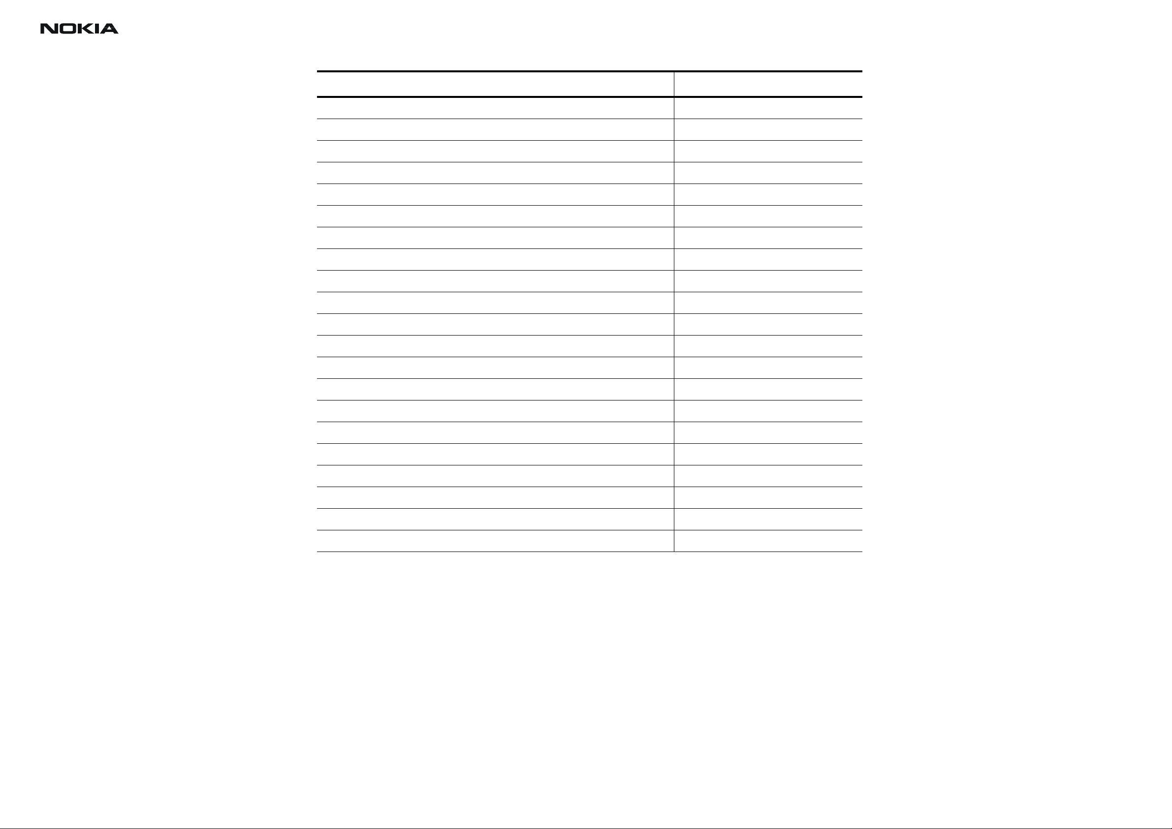
Table of Contents Page
BB/RF connection block diagram v.0.0 ed.79 3
Mjölner IC v.0.0 ed. 229 4
Power amplifier diagram v. 0.0 ed.135 5
Baseband block diagram v. 0.0 ed. 343 6
Audio schematic diagram v. 1.3 ed.48 7
Keyboard diagram v. 1.3 ed.52 8
Flash memory diagram v. 2.0 ed.36 9
Discrete capacitors for memory without VFlash1 v. 1.3 ed.11 10
Discrete power v.1.3 ed.120 11
Light filtering diagram, v.2. 0 RH* 12
Old power discrete capacitors, v. 0.0 ed. 9 13
Power resistor v. 0.0 ed.4 13
RF/BB connection, v. 1.3 ed.28 14
SIM v. 1.3 ed. 32 15
System connector v. 1.3 ed.51 16
UPP 8M diagram, v. 2.0 ed. 107 17
Discrete decoupling capacitors for UPP v,. 1.3 ed.10 18
Audio and Global Ground v. 0.0 RH* 18
Component layout 1AW_07a, top side 19
Component layout 1AW_07a, bottom side 20
Test Points, Baseband 21
Issue 1 10/2003 Copyright © Nokia 2003. All rights reserved. Page A-2
Page 3
Customer Care Solutions Schematics / Layouts 1AW_09 module RH-18/36/38
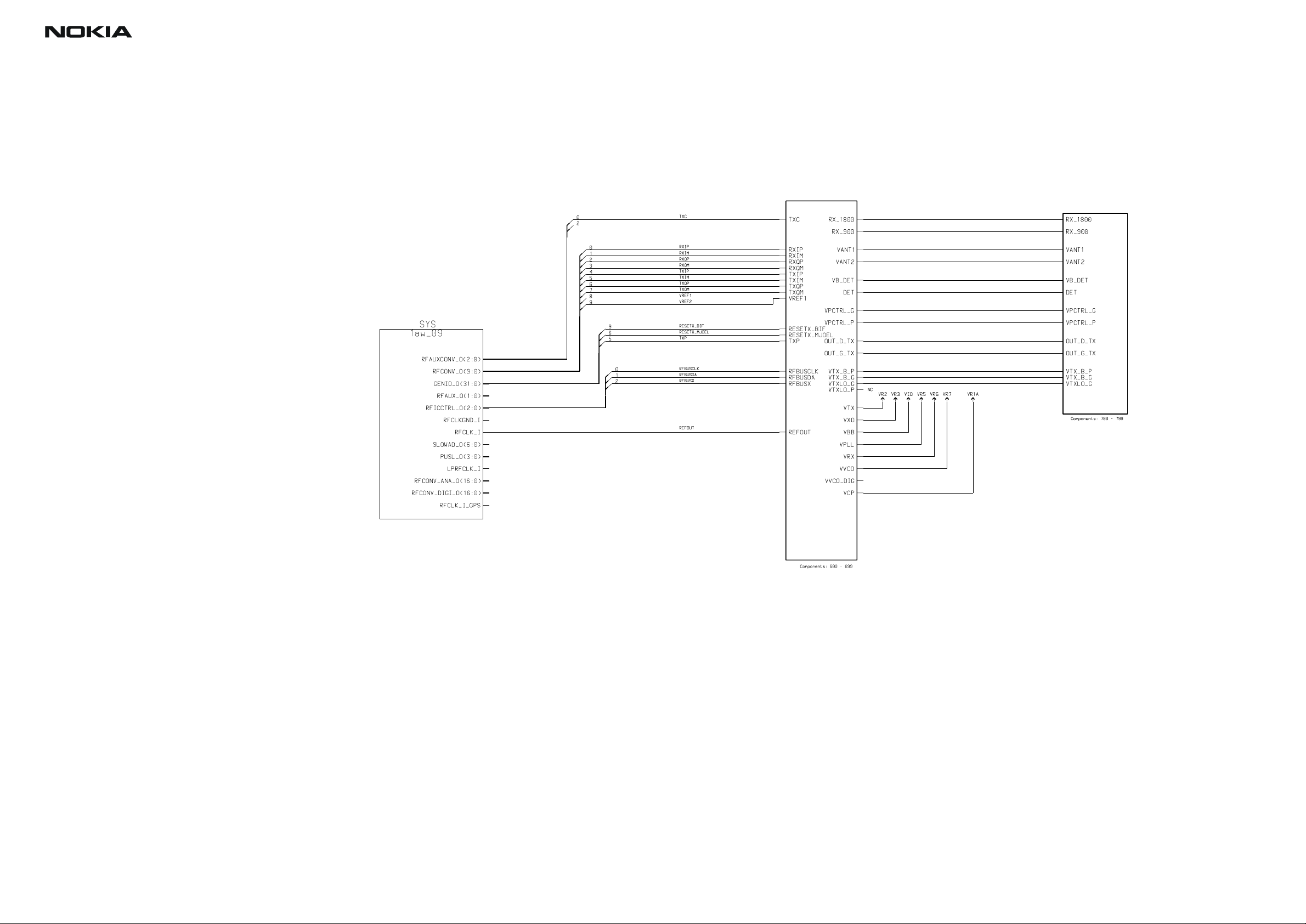
BB/RF connection block diagram v.0.0 ed.79
MJOLNER
POWER_AMP
Issue 1 10/2003 Copyright © Nokia 2003. All rights reserved. Page A-3
Page 4
Customer Care Solutions Schematics / Layouts 1AW_09 module RH-18/36/38
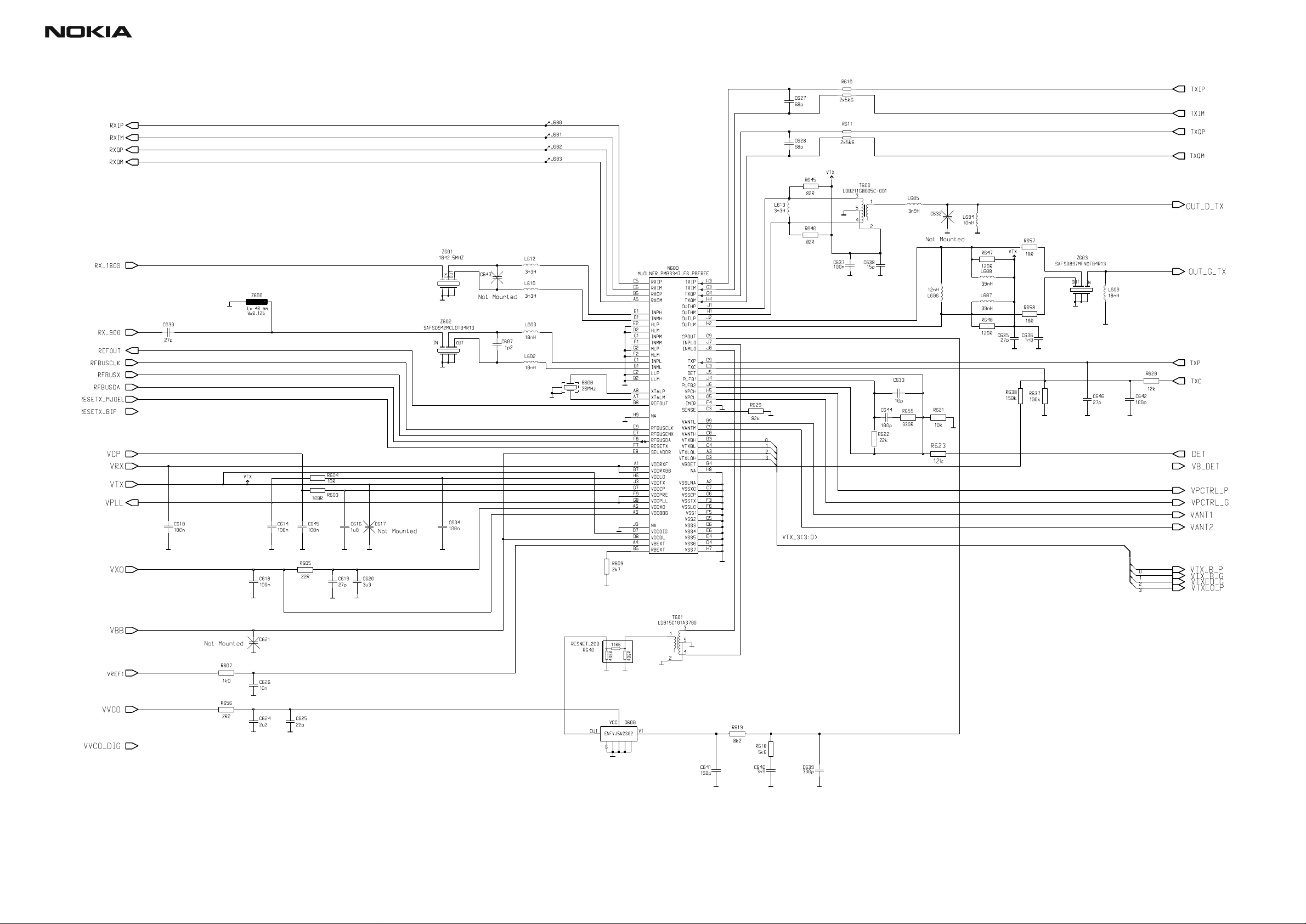
Mjölner IC v.0.0 ed. 229
Issue 1 10/2003 Copyright © Nokia 2003. All rights reserved. Page A-4
Page 5
Customer Care Solutions Schematics / Layouts 1AW_09 module RH-18/36/38
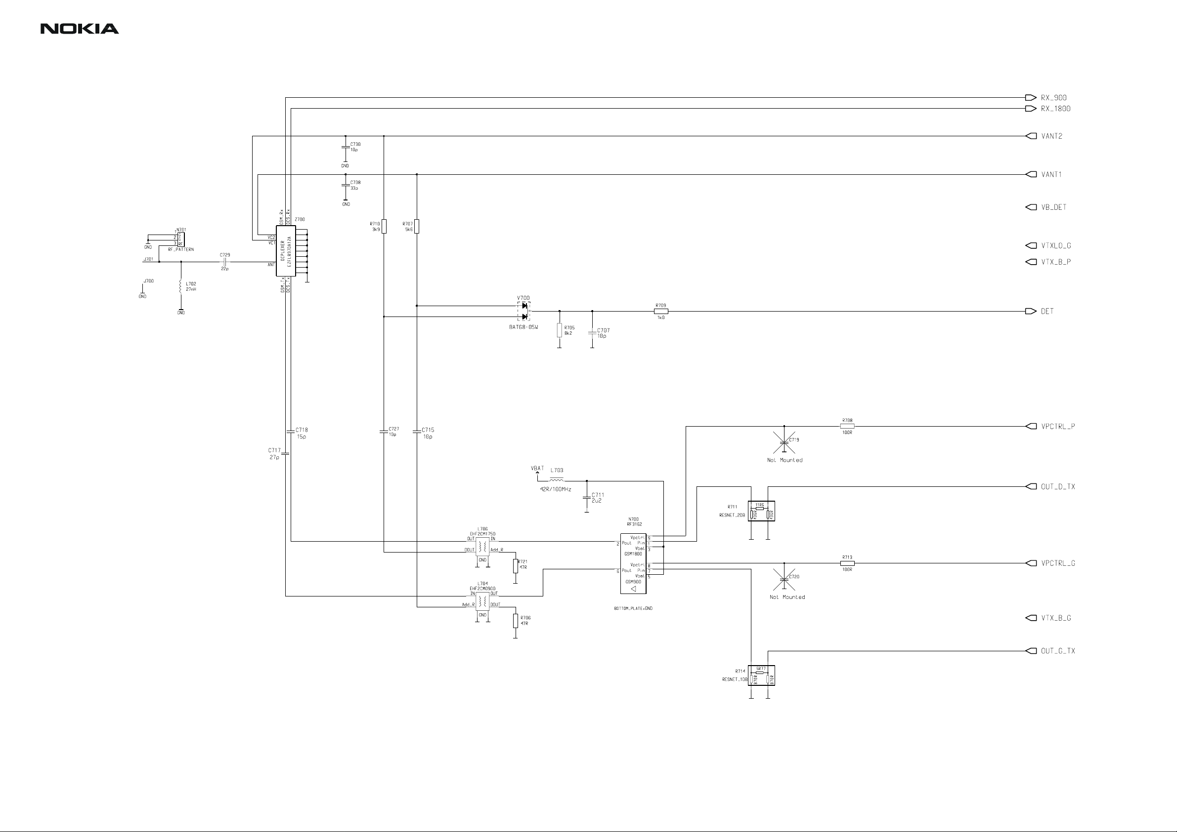
Power amplifier diagram v. 0.0 ed.135
900
1800
Issue 1 10/2003 Copyright © Nokia 2003. All rights reserved. Page A-5
Page 6
Customer Care Solutions Schematics / Layouts 1AW_09 module RH-18/36/38
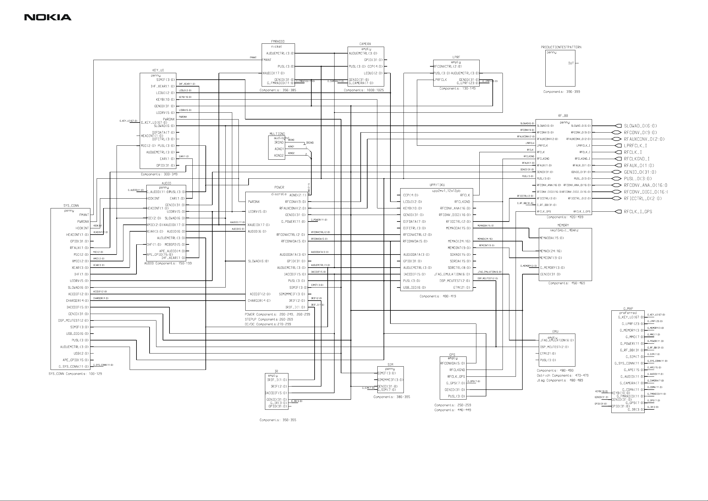
Baseband block diagram v. 0.0 ed. 343
Issue 1 10/2003 Copyright © Nokia 2003. All rights reserved. Page A-6
Page 7
Customer Care Solutions Schematics / Layouts 1AW_09 module RH-18/36/38
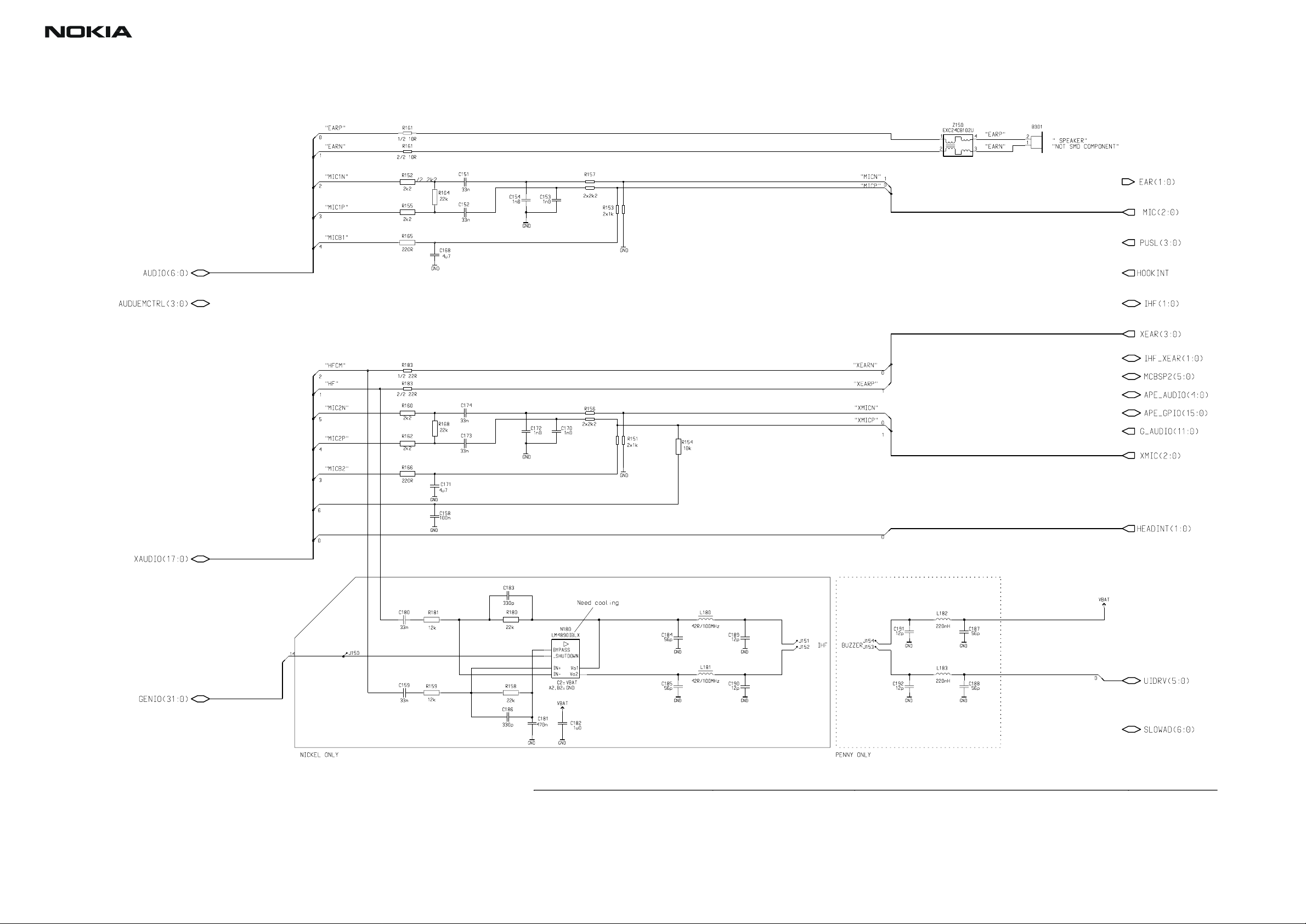
Audio schematic diagram v. 1.3 ed.48
Issue 1 10/2003 Copyright © Nokia 2003. All rights reserved. Page A-7
Page 8

Customer Care Solutions Schematics / Layouts 1AW_09 module RH-18/36/38
03
yy
Keyboard diagram v. 1.3 ed.52
Copyright (C) Nokia Corporation. All rights reserved.
THIS DRAWING IS PROTECTED BY COPYRIGHT AS AN UNPUBLISHED WORK.
UNAUTHORIZED REPRODUCTION OF THIS DRAWING IS NOT PERMITTED.
THIS DRAWING CONTAINS PROPRIETARY AND CONFIDENTIAL INFORMATION.
Name
Keyboard/ User Interface Empty Sheet
Assoc
DCT4 Common Baseband
Design
1aw_b_09
Page
ViewPoint
pcb_design_vpt lob 26 Aug 20
Appr
Des.
Dr.
ArKa
dd-mmm-
30-Dec-98
Issue 1 10/2003 Copyright © Nokia 2003. All rights reserved. Page A-8
Page 9

Customer Care Solutions Schematics / Layouts 1AW_09 module RH-18/36/38
Flash memory diagram v. 2.0 ed.36
Issue 1 10/2003 Copyright © Nokia 2003. All rights reserved. Page A-9
Page 10

Customer Care Solutions Schematics / Layouts 1AW_09 module RH-18/36/38
Discrete capacitors for memory without VFlash1 v. 1.3 ed.11
Issue 1 10/2003 Copyright © Nokia 2003. All rights reserved. Page A-
Page 11

Customer Care Solutions Schematics / Layouts 1AW_09 module RH-18/36/38
Discrete power v.1.3 ed.120
Copyright (C) Nokia Corporation. All rights reserved.
THIS DRAWING IS PROTECTED BY COPYRIGHT AS AN UNPUBLISHED WORK.
UNAUTHORIZED REPRODUCTION OF THIS DRAWING IS NOT PERMITTED.
THIS DRAWING CONTAINS PROPRIETARY AND CONFIDENTIAL INFORMATION.
Name
Discrete Power Management
Assoc
DCT4 Common Baseband
Design
1aw_09
Page
ViewPoint
pcb_design_vpt 63010 28 Feb 03
Appr
Des.
Dr.
ArKa
dd-mmm-yy
08-Jul-97
Issue 1 10/2003 Copyright © Nokia 2003. All rights reserved. Page A-
Page 12

Customer Care Solutions Schematics / Layouts 1AW_09 module RH-18/36/38
Light filtering diagram, v.2. 0 RH*
Issue 1 10/2003 Copyright © Nokia 2003. All rights reserved. Page A-
Page 13

Customer Care Solutions Schematics / Layouts 1AW_09 module RH-18/36/38
Old power discrete capacitors, v. 0.0 ed. 9
SIMIODA_IN SIMIODA_OUT
CCP
CCN
VPUMP
Power resistor v. 0.0 ed.4
RES_OUTRES_IN
Issue 1 10/2003 Copyright © Nokia 2003. All rights reserved. Page A-
Page 14

Customer Care Solutions Schematics / Layouts 1AW_09 module RH-18/36/38
RF/BB connection, v. 1.3 ed.28
RFCONV/RFCONV_O: 0: RXIP
0
1
2
3
4
5
6
7
8
9
0
1
2
3
4
5
6
7
8
9
1: RXIM
2: RXQP
3: RXQM
4: TXIP
5: TXIM
6: TXQP
7: TXQM
9: VREFRF01
J424
13
5
6
7
8
9
10
11
12
0
1
2
J422
J423J421
0
1
2
13
5
6
7
8
9
10
11
12
0
1
2
0
1
2
GENIO/GENIO_O
RFAUXCONV/RFAUXCONV_O
RFICCNTRL/RFICCNTR_O
5: TXP
6: RESETX_MJOEL
9: RESETX_BIF
0: TXC
2: BU_AFC
0: RFBUSCLK
1: RFBUSDA
2: RFBUSEN1
GND
0
1
5
6
R420
1k0
Copyright (C) Nokia Corporation. All rights reserved.
THIS DRAWING IS PROTECTED BY COPYRIGHT AS AN UNPUBLISHED WORK.
UNAUTHORIZED REPRODUCTION OF THIS DRAWING IS NOT PERMITTED.
GND
R426
1k0
C426
1n0
C420
47p
ISET
R422
GND
27k
0
1
5
6
CONSTANT CURRENT SET RESISTOR
FOR RF POWER AMPLIFIER
(see UEM sheet)
Name
Assoc
Design
RF/BB empty sheet
DCT4 Common Baseband
1aw_09
ViewPoint
pcb_design_vpt lob
Appr
Des.
Dr.
ArKa
Issue 1 10/2003 Copyright © Nokia 2003. All rights reserved. Page A-
Page 15

Customer Care Solutions Schematics / Layouts 1AW_09 module RH-18/36/38
SIM v. 1.3 ed. 32
Issue 1 10/2003 Copyright © Nokia 2003. All rights reserved. Page A-
Page 16

Customer Care Solutions Schematics / Layouts 1AW_09 module RH-18/36/38
System connector v. 1.3 ed.51
Issue 1 10/2003 Copyright © Nokia 2003. All rights reserved. Page A-
Page 17

Customer Care Solutions Schematics / Layouts 1AW_09 module RH-18/36/38
UPP 8M diagram, v. 2.0 ed. 107
Issue 1 10/2003 Copyright © Nokia 2003. All rights reserved. Page A-
Page 18

Customer Care Solutions Schematics / Layouts 1AW_09 module RH-18/36/38
Discrete decoupling capacitors for UPP v,. 1.3 ed.10
Audio and Global Ground v. 0.0 RH*
Issue 1 10/2003 Copyright © Nokia 2003. All rights reserved. Page A-
Page 19

Customer Care Solutions Schematics / Layouts 1AW_09 module RH-18/36/38
Component layout 1AW_07a, top side
Issue 1 10/2003 Copyright © Nokia 2003. All rights reserved. Page A-
Page 20

Customer Care Solutions Schematics / Layouts 1AW_09 module RH-18/36/38
Component layout 1A W_07a, bottom side
Issue 1 10/2003 Copyright © Nokia 2003. All rights reserved. Page A-
Page 21

Customer Care Solutions Schematics / Layouts 1AW_09 module RH-18/36/38
Test Points, Baseband
Issue 1 10/2003 Copyright © Nokia 2003. All rights reserved. Page A-
Page 22

Customer Care Solutions Schematics / Layouts 1AW_09 module RH-18/36/38
Issue 1 10/2003 Copyright © Nokia 2003. All rights reserved. Page A-
 Loading...