

DATA SHEET
PHOTOCOUPLER
PS9513,PS9513L1,PS9513L2,PS9513L3
1 Mbps, OPEN COLLECTOR OUTPUT, FOR GATE DRIVE INTERFACE
INTELLIGENT POWER MODULE
8 mm CREEPAGE 8-PIN DIP HIGH-SPEED PHOTOCOUPLER
DESCRIPTION
The PS9513, PS9513L1, PS9513L2 and PS9513L3 are optically coupled isolators containing a GaAlAs LED on the
input side and a photo diode and a signal processing circuit on the output side on one chip.
The PS9513 is designed specifically for high common mode transient immunity (CMR) and low pulse width
distortion with operating temperature. It is suitable for IPM drive.
The PS9513L1 is lead bending type for long creepage distance.
The PS9513L2 is lead bending type for long creepage distance (Gull-wing) for surface mount.
The PS9513L3 is lead bending type (Gull-wing) for surface mounting.
FEATURES
• Long creepage distance (8 mm MIN. : PS9513L1, PS9513L2)
• High common mode transient immunity (CM
• High-speed response (t
• Maximum propagation delays (t
• Pulse width distortion ( | t
PHL = 500 ns MAX., tPLH = 750 ns MAX.)
PLH − tPHL = 270 ns TYP.)
PHL − tPLH | = 270 ns TYP.)
H, CML = ±15 kV/
μ
s MIN.)
• Open collector output
• Ordering number of tape product : PS9513L2-E3 : 1 000 pcs/reel
: PS9513L3-E3 : 1 000 pcs/reel
• Pb-Free product
• Safety standards
• UL approved: File No. E72422
• CSA approved: No. CA 101391
• BSI approved: No. 8937, 8938
• SEMKO approved: No. 615433
• NEMKO approved: No. P06207243
• DEMKO approved: No. 314091
• FIMKO approved: No. FI 22827
• DIN EN60747-5-2 (VDE0884 Part2) approved (Option)
APPLICATIONS
• IPM Driver
• General purpose inverter
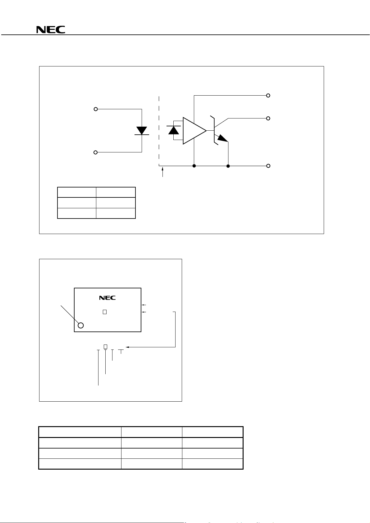
PIN CONNECTIONS
(Top View)
8
7
243
1
5
6
−NEPOC Series−
1. NC
2. Anode
3. Cathode
4. NC
5. GND
6. V
O
7. NC
8. V
CC
The information in this document is subject to change without notice. Before using this document, please
confirm that this is the latest version.
Not all products and/or types are available in every country. Please check with an NEC Electronics
sales representative for availability and additional information.
Document No. PN10679EJ02V0DS (2nd edition)
Date Published August 2008 NS
Printed in Japan
The revised points can be easily searched by copying an "<R>" in the PDF file and specifying it in the "Find what:" field.
The mark <R> shows major revised points.
2007, 2008
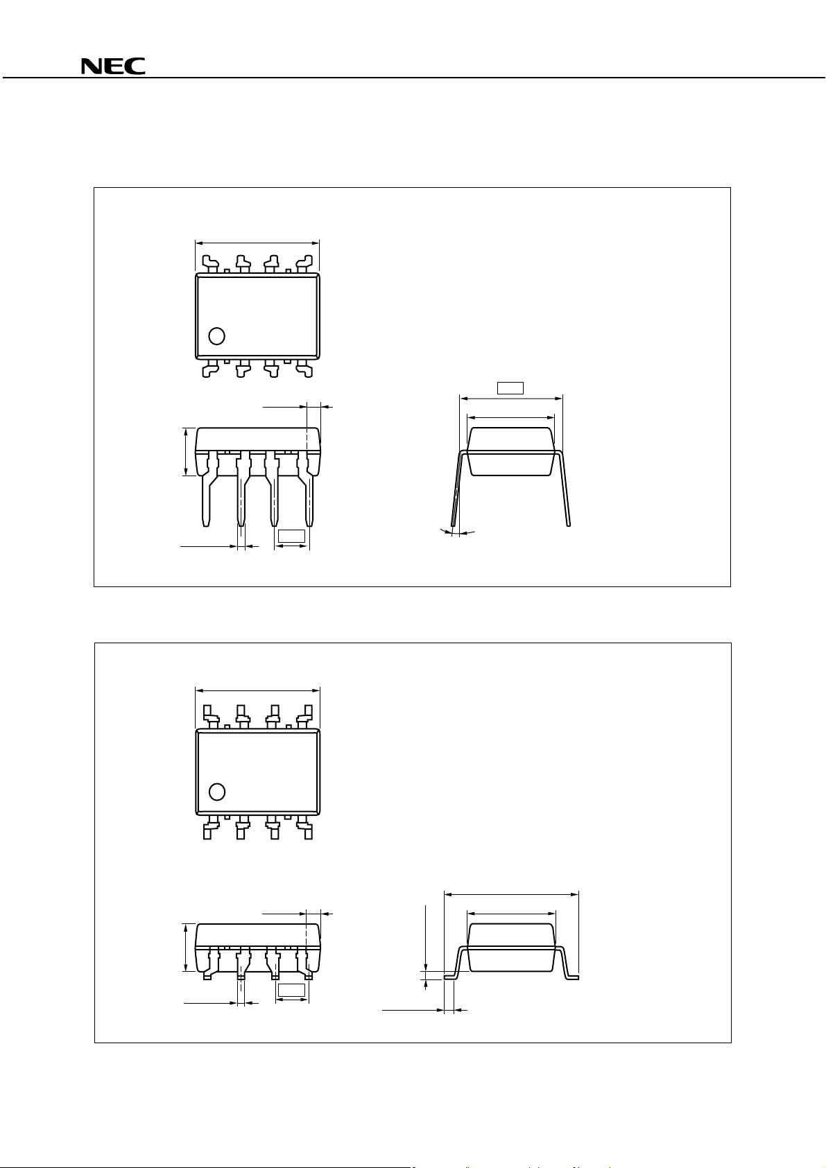
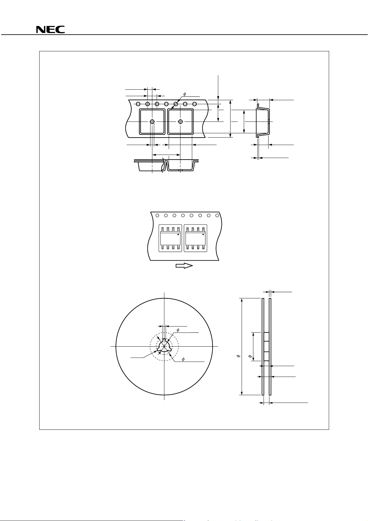
PACKAGE DIMENSIONS (UNIT: mm)
DIP Type
+0.5
9.25
–0.25
PS9513,PS9513L1,PS9513L2 PS9513L3
PS9513
+0.4
1.01
–0.2
3.5±0.2
0.5±0.15
2.54
Lead Bending Type (Gull-wing) For Surface Mount
PS9513L3
9.25
+0.5
–0.25
7.62
6.5
0 to 15˚
+0.5
–0.1
2
3.5±0.2
0.5±0.15
1.01
+0.4
–0.2
2.54
0.635±0.15
0.74±0.25
Data Sheet PN10679EJ02V0DS
9.65±0.4
+0.5
6.5
–0.1
PS9513,PS9513L1,PS9513L2 PS9513L3
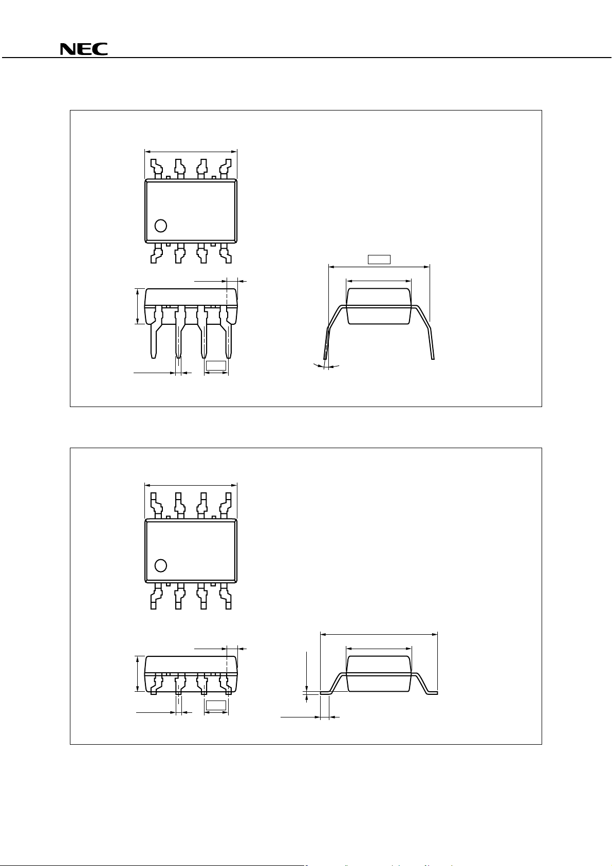
Lead Bending Type For Long Creepage Distance
PS9513L1
+0.5
9.25
–0.25
+0.4
1.01
–0.2
3.5±0.2
10.16
6.5
+0.5
–0.1
0.5±0.15
2.54
0 to 15˚
Lead Bending Type For Long Creepage Distance (Gull-wing) For Surface Mount
PS9513L2
11.8±0.4
+0.5
6.5
–0.1
9.25
+0.5
–0.25
1.01
+0.4
–0.2
3.5±0.2
0.5±0.15
2.54
0.25±0.2
0.9±0.25
Data Sheet PN10679EJ02V0DS
3
PS9513,PS9513L1,PS9513L2 PS9513L3
FUNCTIONAL DIAGRAM
8
2
6
3
5
Shield
<R>
LED
ON L
OFF
MARKING EXAMPLE
No. 1 pin
Mark
N 831
N
Output
H
9513
8
31
Year Assembled
(Last 1 Digit)
In-house Code
(L or T)
Rank Code
Type Number
Assembly Lot
Week Assembled
PHOTOCOUPLER CONSTRUCTION
Parameter PS9513, PS9513L3 PS9513L1, PS9513L2
Air Distance (MIN.) 7 mm 8 mm
Outer Creepage Distance (MIN.) 7 mm 8 mm
Isolation Distance (MIN.) 0.4 mm 0.4 mm
4
Data Sheet PN10679EJ02V0DS
PS9513,PS9513L1,PS9513L2 PS9513L3
ORDERING INFORMATION
Part Number Order Number Solder Plating
Specification
PS9513 PS9513-AX Pb-Free Magazine case 50 pcs Standard products PS9513
PS9513L1 PS9513L1-AX (Ni/Pd/Au) (UL, CSA, BSI, PS9513L1
PS9513L2 PS9513L2-AX SEMKO, NEMKO, PS9513L2
PS9513L3 PS9513L3-AX DEMKO, FIMKO PS9513L3
PS9513L2-E3 PS9513L2-E3-AX Embossed Tape 1 000 pcs/reel approved) PS9513L2
PS9513L3-E3 PS9513L3-E3-AX PS9513L3
PS9513-V PS9513-V-AX Magazine case 50 pcs DIN EN60747-5-2 PS9513
PS9513L1-V PS9513L1-V-AX (VDE0884 Part2) PS9513L1
PS9513L2-V PS9513L2-V-AX Approved (Option) PS9513L2
PS9513L3-V PS9513L3-V-AX PS9513L3
PS9513L2-V-E3 PS9513L2-V-E3-AX
PS9513L3-V-E3 PS9513L3-V-E3-AX PS9513L3
Embossed Tape 1 000 pcs/reel PS9513L2
*1 For the application of the Safety Standard, following part number should be used.
Packing Style Safety Standard
Approval
Application Part
Number*
1
Data Sheet PN10679EJ02V0DS
5
PS9513,PS9513L1,PS9513L2 PS9513L3
ABSOLUTE MAXIMUM RATINGS (TA = 25°C, unless otherwise specified)
Parameter Symbol Ratings Unit
Diode Forward Current
Reverse Voltage VR 5.0 V
Detector
Output Voltage VO −0.5 to +35 V
Output Current IO 15 mA
Power Dissipation
Isolation Voltage
Operating Ambient Temperature TA −40 to +100 °C
Storage Temperature Tstg −55 to +125 °C
Supply Voltage VCC −0.5 to +35 V
*3
BV 5 000 Vr.m.s.
*1 Reduced to 0.33 mA/°C at T
*2 Reduced to 2.0 mW/°C at T
*3 AC voltage for 1 minute at T
Pins 1-4 shorted together, 5-8 shorted together.
RECOMMENDED OPERATING CONDITIONS
Parameter Symbol MIN. TYP. MAX. Unit
*1
IF 25 mA
*2
PC 100 mW
A = 70°C or more.
A = 70°C or more.
A = 25°C, RH = 60% between input and output.
Forward Current IF 10 20 mA
Output Voltage VO 0 30 V
Supply Voltage VCC 4.5 15 30 V
Input Voltage VF 0 0.8 V
6
Data Sheet PN10679EJ02V0DS
PS9513,PS9513L1,PS9513L2 PS9513L3
ELECTRICAL CHARACTERISTICS (TA = −40 to +100°C, VCC = 15 V, unless otherwise specified)
Parameter Symbol Conditions MIN. TYP.*1 MAX. Unit
Diode Forward Voltage VF IF = 10 mA 1.3 1.65 2.1 V
Reverse Current IR VR = 3 V 200
Terminal Capacitance Ct V = 0 V, f = 1 MHz, TA = 25°C 30 pF
Detector Low Level Output Voltage VOL IF = 10 mA, IOL = 2.4 mA 0.13 0.6 V
High Level Output Current IOH VCC = 30 V, VF = 0.8 V 1.0 50
High Level Supply Current ICCH VCC = 30 V, VF = 0.8 V, VO = open 0.6 1.3 mA
Low Level Supply Current ICCL VCC = 30 V, IF = 10 mA, VO = open 0.6 1.3 mA
Coupled Threshold Input Current
IFHL VO = 0.8 V, IO = 0.75 mA 0.86 5.0 mA
(H → L)
Current Transfer Ratio (IC/IF) CTR IF = 10 mA, VO = 0.6 V 44 110 %
11
Isolation Resistance RI-O VI-O = 1 kVDC, RH = 40 to 60%,
A = 25°C
T
10
Isolation Capacitance CI-O V = 0 V, f = 1 MHz, TA = 25°C 0.7 pF
Propagation Delay Time
Propagation Delay Time
(H → L)
(L → H)
*2
*2
Maximum Propagation
t
PHL IF = 10 mA, RL = 20 kΩ, CL = 100 pF,
THHL = 1.5 V, VTHLH = 2.0 V
V
t
PLH
tPLH−tPHL −200 270 650
250 500 ns
520 750
Delays
Pulse Width Distortion
(PWD)
*2
Common Mode
Transient Immunity at High
Level Output
*3
Common Mode
Transient Immunity at Low
Level Output
*3
|t
PHL−tPLH| 270 650
H TA = 25°C, IF = 0 mA, VO > 3.0 V,
CM
CM = 1.5 kV, RL = 20 kΩ,
V
L = 100 pF
C
L TA = 25°C, IF = 10 mA, VO < 1.0 V,
CM
CM = 1.5 kV, RL = 20 kΩ,
V
L = 100 pF
C
15 kV/
15 kV/
μ
A
μ
A
Ω
μ
s
μ
s
Data Sheet PN10679EJ02V0DS
7
*1 Typical values at TA = 25°C.
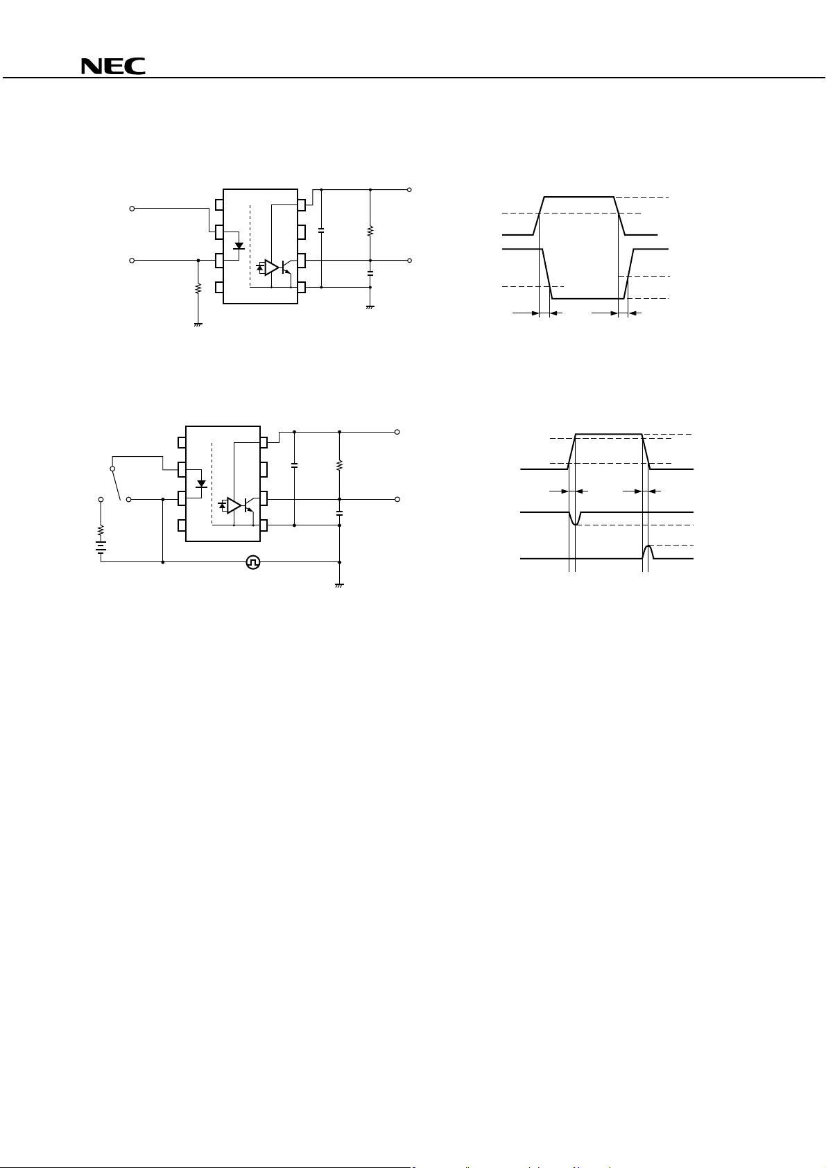
*2 Test circuit for propagation delay time
Pulse input (I
(PW = 10 s,
Duty cycle = 1/10)
Input
(monitor)
F
μ
= 10 mA)
47 Ω
GND
μ
0.1 F
PS9513,PS9513L1,PS9513L2 PS9513L3
CC
= 15 V
V
RL = 20 kΩ
V
O
CL = 100 pF
(monitor)
THHL
= 1.5 V
V
Input
Output
t
PHL
t
PLH
50% I
IF (ON)
F
(ON)
15 V
V
THLH
OL
V
= 2.0 V
CL includes probe and stray wiring capacitance.
*3 Test circuit for common mode transient immunity
V
CC
F
SW I
BA
GND
0.1 F
μ
R
L
= 20 kΩ
CL = 100 pF
= 15 V
VO (monitor)
VCM 90%
10%
t
V
O
(Switch A: IF = 0 mA)
O
V
(Switch B: IF = 10 mA)
r
t
f
1.5 kV
0 V
V
3.0 V
1.0 V
V
CL includes probe and stray wiring capacitance.
USAGE CAUTIONS
1. This product is weak for static electricity by designed with high-speed integrated circuit so protect against static
electricity when handling.
2. By-pass capacitor of more than 0.1
distance between the leads of the photocoupler and capacitor is no more than 10 mm.
3. Avoid storage at a high temperature and high humidity.
μ
F is used between VCC and GND near device. Also, ensure that the
OH
OL
8
Data Sheet PN10679EJ02V0DS

PS9513,PS9513L1,PS9513L2 PS9513L3
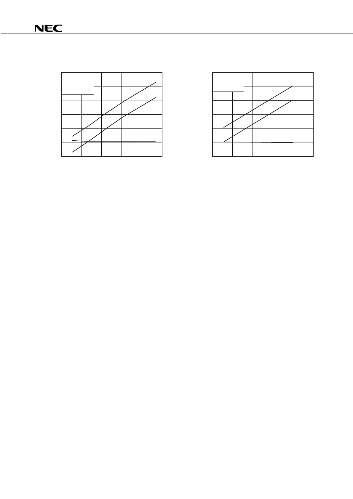
TYPICAL CHARACTERISTICS (TA = 25°C, unless otherwise specified)
MAXIMUM FORWARD CURRENT
vs. AMBIENT TEMPERATURE
40
35
30
25
20
DETECTOR POWER DISSIPATION
vs. AMBIENT TEMPERATURE
150
100
15
10
Maximum Forward Current IF (mA)
100
10
0.1
Forward Current IF (mA)
0.01
5
25 50 75 100 1250
Ambient Temperature TA (˚C)
FORWARD CURRENT vs.
FORWARD VOLTAGE
TA = +100˚C
+85˚C
1
1.0
1.2 1.4 1.6 1.8 2.0 2.2 2.4
Forward Voltage VF (V)
+50˚C
+25˚C
0˚C
–20˚C
–40˚C
50
Detector Power Dissipation PC (mW)
25 50 75 100 1250
Ambient Temperature TA (˚C)
SUPPLY CURRENT vs.
AMBIENT TEMPERATURE
1.20
1.00
CCL (mA)
0.80
0.60
0.40
0.20
High Level Supply Current ICCH (mA),
Low Level Supply Current I
0
–50 –25 0 25 50 75 100
Ambient Temperature TA (˚C)
V
V
CCH : VF = 0.8 V,
I
CCL : IF = 10 mA
I
CC = 30 V,
O = Open,
I
CCL
ICCH
THRESHOLD INPUT CURRENT vs.
AMBIENT TEMPERATURE
5
4
3
2
1
Threshold Input Current IFHL (mA)
0
–50 –25 0 25 50 75 100
Ambient Temperature TA (˚C)
Remark The graphs indicate nominal characteristics.
VCC = 15 V,
O = 0.8 V,
V
O = 0.75 mA
I
Data Sheet PN10679EJ02V0DS
LOW LEVEL OUTPUT VOLTAGE vs.
AMBIENT TEMPERATURE
0.6
0.5
0.4
0.3
0.2
0.1
Low Level Output Voltage VOL (V)
0
–50 –25
Ambient Temperature TA (˚C)
250 50 75 100
CC = 15 V,
V
F = 10 mA,
I
O = 2.4 mA
I
9

OUTPUT CURRENT vs. FORWARD CURRENT
14
A
= +100˚C
12
10
(mA)
O
T
+25˚C
8
6
–40˚C
4
Output Current I
2
0 5 10 15 20
Forward Current IF (mA)
O
V
= 0.6 V
PROPAGATION DELAY TIME,
MAXIMUM PROPAGATION DELAYS
vs. FORWARD CURRENT
700
(ns)
PHL
600
– t
(ns),
PLH
PLH
500
, t
PHL
400
t
PLH
t
PLH
– t
PHL
300
200
100
0 5 10 15 20
Maximum Propagation Delays t
Propagation Delay Time t
t
PHL
VCC = 15 V,
C
L
= 100 pF,
R
L
= 20 kΩ
Forward Current IF (mA)
PROPAGATION DELAY TIME,
PULSE WIDTH DISTORTION
vs. AMBIENT TEMPERATURE
700
(ns)
PLH
600
– t
(ns),
PHL
PLH
500
, t
PHL
400
300
200
V
CC
= 15 V,
I
F
= 10 mA,
100
L
= 100 pF,
C
R
L
= 20 kΩ
0
Pulse Width Distortion (PWD) t
Propagation Delay Time t
–40 –20 0 20 40 60 80 100
Ambient Temperature TA (˚C)
Remark The graphs indicate nominal characteristics.
t
PLH
PWD
PHL
t
PS9513,PS9513L1,PS9513L2 PS9513L3
OUTPUT CURRENT vs.
AMBIENT TEMPERATURE
1.10
F
= 10 mA,
I
V
O
1.05
1.00
0.95
0.90
(Value relative to 25˚C)
O
0.85
0.80
0.75
0.70
Output Current I
1 800
(ns)
PHL
1 600
– t
(ns),
1 400
PLH
PLH
, t
1 200
PHL
1 000
800
600
400
200
Maximum Propagation Delays t
Propagation Delay Time t
1 800
1 600
(ns)
PLH
1 400
, t
PHL
1 200
1 000
800
600
400
200
Propagation Delay Time t
= 0.6 V
–40 –20 0 20 40 60 80 100
Ambient Temperature TA (˚C)
PROPAGATION DELAY TIME,
MAXIMUM PROPAGATION DELAYS
vs. SUPPLY VOLTAGE
IF = 10 mA,
C
L
= 100 pF,
R
L
= 20 kΩ
t
PLH
t
PHL
t
PLH
– t
PHL
010203040
Supply Voltage VCC (V)
PROPAGATION DELAY TIME vs.
LOAD CAPACITANCE
VCC = 15 V,
I
F
= 10 mA,
R
L
= 20 kΩ
0 100 200 300 400
Load Capacitance CL (pF)
t
PLH
PHL
t
500
10
Data Sheet PN10679EJ02V0DS
PS9513,PS9513L1,PS9513L2 PS9513L3
PROPAGATION DELAY TIME,
MAXIMUM PROPAGATION DELAYS
vs. LOAD RESISTANCE
1 200
(ns)
VCC = 15 V,
PHL
I
F
800
= 10 mA,
C
L
= 100 pF
(ns),
PLH
, t
PHL
1 000
– t
PLH
600
400
200
010203040
Maximum Propagation Delays t
Propagation Delay Time t
Load Resistance RL (kΩ)
Remark The graphs indicate nominal characteristics.
t
PLH
t
PLH
– t
PHL
PHL
t
50
PROPAGATION DELAY TIME,
MAXIMUM PROPAGATION DELAYS
vs. LOAD RESISTANCE
600
(ns)
VCC = 5 V,
PHL
– t
(ns),
PLH
PLH
, t
PHL
Maximum Propagation Delays t
Propagation Delay Time t
F
= 10 mA,
I
500
C
L
= 15 pF
400
300
200
100
0 5 10 15 20
Load Resistance RL (kΩ)
t
PLH
t
PLH
– t
PHL
PHL
t
25
Data Sheet PN10679EJ02V0DS
11

TAPING SPECIFICATIONS (UNIT: mm)
Outline and Dimensions (Tape)
PS9513,PS9513L1,PS9513L2 PS9513L3
2.0±0.1
4.0±0.1
2.05±0.05
Tape Direction
12.0±0.1
+0.1
1.5
–0
10.7±0.1
PS9513L2-E3
1.75±0.1
11.5±0.1
24.0±0.3
4.5 MAX.
12.8±0.1
4.1±0.1
0.3±0.05
Pull-out direction
Outline and Dimensions (Reel)
2.0±0.5
13.0±0.2
R 1.0
Packing: 1 000 pcs/reel
21.0±0.8
330±2.0
100±1.0
2.0±0.5
25.5±1.0
29.5±1.0
23.9 to 27.4
Outer edge of
flange
12
Data Sheet PN10679EJ02V0DS
Outline and Dimensions (Tape)
PS9513,PS9513L1,PS9513L2 PS9513L3
Tape Direction
2.0±0.1
4.0±0.1
1.55±0.1
12.0±0.1
PS9513L3-E3
1.5
+0.1
–0
10.3±0.1
1.75±0.1
7.5±0.1
16.0±0.3
5.3 MAX.
10.4±0.1
4.75±0.1
0.35±0.05
Outline and Dimensions (Reel)
R 1.0
Packing: 1 000 pcs/reel
2.0±0.5
13.0±0.2
21.0±0.8
330±2.0
100±1.0
2.0±0.5
17.5±1.0
21.5±1.0
15.9 to 19.4
Outer edge of
flange
Data Sheet PN10679EJ02V0DS
13

PS9513,PS9513L1,PS9513L2 PS9513L3
RECOMMENDED MOUNT PAD DIMENSIONS (UNIT: mm)
D
CB
Part Number
PS9513L2
PS9513L3
A
Lead Bending
lead bending type (Gull-wing)
for long creepage distance (surface mount)
lead bending type (Gull-wing)
for surface mount
A
10.2
8.2
B
2.54
2.54
C
1.7
1.7
D
2.2
2.2
14
Data Sheet PN10679EJ02V0DS
PS9513,PS9513L1,PS9513L2 PS9513L3
NOTES ON HANDLING
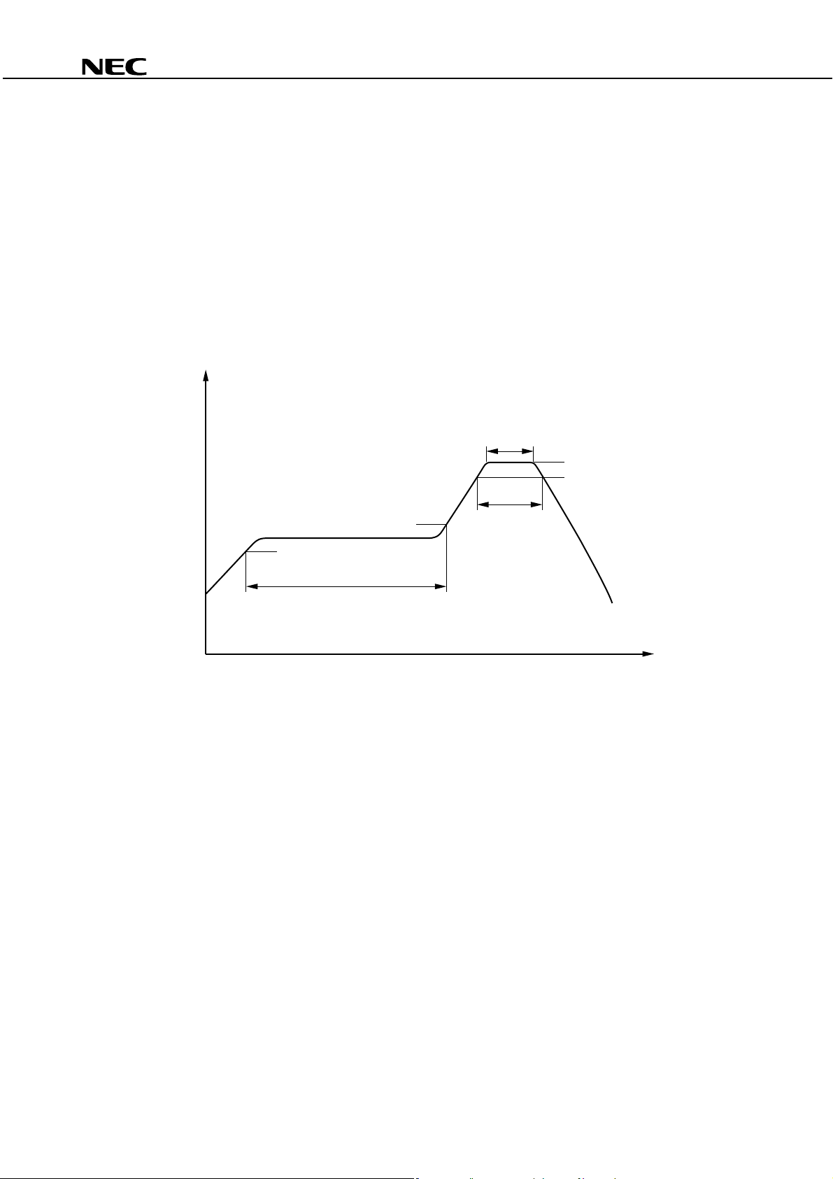
1. Recommended soldering conditions
(1) Infrared reflow soldering
• Peak reflow temperature 260°C or below (package surface temperature)
• Time of peak reflow temperature 10 seconds or less
• Time of temperature higher than 220°C 60 seconds or less
• Time to preheat temperature from 120 to 180°C 120±30 s
• Number of reflows Three
• Flux Rosin flux containing small amount of chlorine (The flux with a
maximum chlorine content of 0.2 Wt% is recommended.)
Recommended Temperature Profile of Infrared Reflow
(heating)
to 10 s
260˚C MAX.
220˚C
to 60 s
180˚C
120˚C
Package Surface Temperature T (˚C)
120±30 s
(preheating)
Time (s)
(2) Wave soldering
• Temperature 260°C or below (molten solder temperature)
• Time 10 seconds or less
• Preheating conditions 120°C or below (package surface temperature)
• Number of times One (Allowed to be dipped in solder including plastic mold portion.)
• Flux Rosin flux containing small amount of chlorine (The flux with a maximum chlorine
content of 0.2 Wt% is recommended.)
(3) Soldering by soldering iron
• Peak temperature (lead part temperature) 350°C or below
• Time (each pins) 3 seconds or less
• Flux Rosin flux containing small amount of chlorine (The flux with a
maximum chlorine content of 0.2 Wt% is recommended.)
(a) Soldering of leads should be made at the point 1.5 to 2.0 mm from the root of the lead.
(b) Please be sure that the temperature of the package would not be heated over 100°C.
Data Sheet PN10679EJ02V0DS
15

<R>
PS9513,PS9513L1,PS9513L2 PS9513L3
(4) Cautions
• Fluxes
Avoid removing the residual flux with freon-based and chlorine-based cleaning solvent.
2. Cautions regarding noise
Be aware that when voltage is applied suddenly between the photocoupler’s input and output or between
collector-emitters at startup, the output transistor may enter the on state, even if the voltage is within the absolute
maximum ratings.
USAGE CAUTIONS
1. Protect against static electricity when handling.
2. Avoid storage at a high temperature and high humidity.
16
Data Sheet PN10679EJ02V0DS
PS9513,PS9513L1,PS9513L2 PS9513L3
SPECIFICATION OF VDE MARKS LICENSE DOCUMENT
Parameter Symbol Speck Unit
<R>
Application classification (DIN EN 60664-1 VDE0110 Part 1)
for rated line voltages ≤ 300 Vr.m.s.
for rated line voltages ≤ 600 Vr.m.s.
IV
III
Climatic test class (DIN EN 60664-1 VDE0110) 55/100/21
Dielectric strength
maximum operating isolation voltage
Test voltage (partial discharge test, procedure a for type test and random test)
pr = 1.5 × UIORM, Pd < 5 pC
U
Test voltage (partial discharge test, procedure b for all devices)
pr = 1.875 × UIORM, Pd < 5 pC
U
IORM
U
Upr
U
pr 2 119 Vpeak
1 130
1 695
peak
V
Vpeak
Highest permissible overvoltage UTR 8 000 Vpeak
Degree of pollution (DIN EN 60664-1 VDE0110 Part 1) 2
Clearance distance >8.0 mm
Creepage distance >8.0 mm
Comparative tracking index (DIN IEC 112/VDE 0303 Part 1) CTI 175
Material group (DIN EN 60664-1 VDE0110 Part 1) III a
Storage temperature range Tstg –55 to +125 °C
Operating temperature range TA –40 to +100 °C
Isolation resistance, minimum value
IO = 500 V dc at TA = 25°C
V
IO = 500 V dc at TA MAX. at least 100°C
V
Safety maximum ratings (maximum permissible in case of fault, see thermal
derating curve)
Package temperature
Current (input current I
F, Psi = 0)
Power (output or total power dissipation)
Isolation resistance
V
IO = 500 V dc at TA = Tsi
Ris MIN.
Ris MIN.
Tsi
Isi
Psi
Ris MIN.
10
10
175
400
700
10
12
11
Ω
Ω
°C
mA
mW
9
Ω
Data Sheet PN10679EJ02V0DS
17

PS9513,PS9513L1,PS9513L2 PS9513L3
•
The information in this document is current as of August, 2008. The information is subject to
change without notice. For actual design-in, refer to the latest publications of NEC Electronics data
sheets or data books, etc., for the most up-to-date specifications of NEC Electronics products. Not
all products and/or types are available in every country. Please check with an NEC Electronics sales
representative for availability and additional information.
No part of this document may be copied or reproduced in any form or by any means without the prior
•
written consent of NEC Electronics. NEC Electronics assumes no responsibility for any errors that may
appear in this document.
•
NEC Electronics does not assume any liability for infringement of patents, copyrights or other intellectual
property rights of third parties by or arising from the use of NEC Electronics products listed in this document
or any other liability arising from the use of such products. No license, express, implied or otherwise, is
granted under any patents, copyrights or other intellectual property rights of NEC Electronics or others.
Descriptions of circuits, software and other related information in this document are provided for illustrative
•
purposes in semiconductor product operation and application examples. The incorporation of these
circuits, software and information in the design of a customer's equipment shall be done under the full
responsibility of the customer. NEC Electronics assumes no responsibility for any losses incurred by
customers or third parties arising from the use of these circuits, software and information.
•
While NEC Electronics endeavors to enhance the quality, reliability and safety of NEC Electronics products,
customers agree and acknowledge that the possibility of defects thereof cannot be eliminated entirely. To
minimize risks of damage to property or injury (including death) to persons arising from defects in NEC
Electronics products, customers must incorporate sufficient safety measures in their design, such as
redundancy, fire-containment and anti-failure features.
•
NEC Electronics products are classified into the following three quality grades: "Standard", "Special" and
"Specific".
The "Specific" quality grade applies only to NEC Electronics products developed based on a customerdesignated "quality assurance program" for a specific application. The recommended applications of an NEC
Electronics product depend on its quality grade, as indicated below. Customers must check the quality grade of
each NEC Electronics product before using it in a particular application.
"Standard":
"Special":
"Specific":
Computers, office equipment, communications equipment, test and measurement equipment, audio
and visual equipment, home electronic appliances, machine tools, personal electronic equipment
and industrial robots.
Transportation equipment (automobiles, trains, ships, etc.), traffic control systems, anti-disaster
systems, anti-crime systems, safety equipment and medical equipment (not specifically designed
for life support).
Aircraft, aerospace equipment, submersible repeaters, nuclear reactor control systems, life
support systems and medical equipment for life support, etc.
The quality grade of NEC Electronics products is "Standard" unless otherwise expressly specified in NEC
Electronics data sheets or data books, etc. If customers wish to use NEC Electronics products in applications
not intended by NEC Electronics, they must contact an NEC Electronics sales representative in advance to
determine NEC Electronics' willingness to support a given application.
(Note)
(1)
"NEC Electronics" as used in this statement means NEC Electronics Corporation and also includes its
majority-owned subsidiaries.
(2)
"NEC Electronics products" means any product developed or manufactured by or for NEC Electronics (as
defined above).
M8E 02. 11-1
18
Data Sheet PN10679EJ02V0DS

PS9513,PS9513L1,PS9513L2 PS9513L3
Caution GaAs Products
This product uses gallium arsenide (GaAs).
GaAs vapor and powder are hazardous to human health if inhaled or ingested, so please observe
the following points.
• Follow related laws and ordinances when disposing of the product. If there are no applicable laws
and/or ordinances, dispose of the product as recommended below.
1. Commission a disposal company able to (with a license to) collect, transport and dispose of
materials that contain arsenic and other such industrial waste materials.
2. Exclude the product from general industrial waste and household garbage, and ensure that the
product is controlled (as industrial waste subject to special control) up until final disposal.
• Do not burn, destroy, cut, crush, or chemically dissolve the product.
• Do not lick the product or in any way allow it to enter the mouth.
 Loading...