


PRELIMINARY DATA SHEET
Solid State Relay
OCMOS FET
PS7241E-1A
4-PIN SOP 400 V BREAK DOWN VOLTAGE
1-ch Optical Coupled MOS FET
DESCRIPTION
The PS7241E-1A is an optically coupled element that combines a GaAs infrared LED on the input side with a
normally-open MOS FET on the output side to realize an excellent cost performance.
The small, thin package and high sensitivity of this element makes it ideal for battery-driven mobile devices, and its
small offset voltage at power-on and good linearity are also make it suitable for controlling micro analog signals.
FEATURES
• Small and thin package (4-pin SOP, Height = 2.1 mm)
• 1 channel type (1 a output)
• Designed for AC/DC switching line changer
• Low offset voltage
• Ordering number of taping product: PS7241E-1A-E3, E4, F3, F4
• UL awaiting approval
• BSI awaiting approval
APPLICATIONS
• Laptop PC, PDA
• Modem card
• Telephone, FAX
• Measurement equipment
The information in this document is subject to change without notice. Before using this document, please confirm that
this is the latest version.
Not all devices/types available in every country. Please check with local NEC Compound Semiconductor Devices
representative for availability and additional information.
Document No. PN10459EJ01V0DS (1st edition)
Date Published January 2004 CP(K)
Printed in Japan
NEC Compound Semiconductor Devices 2004
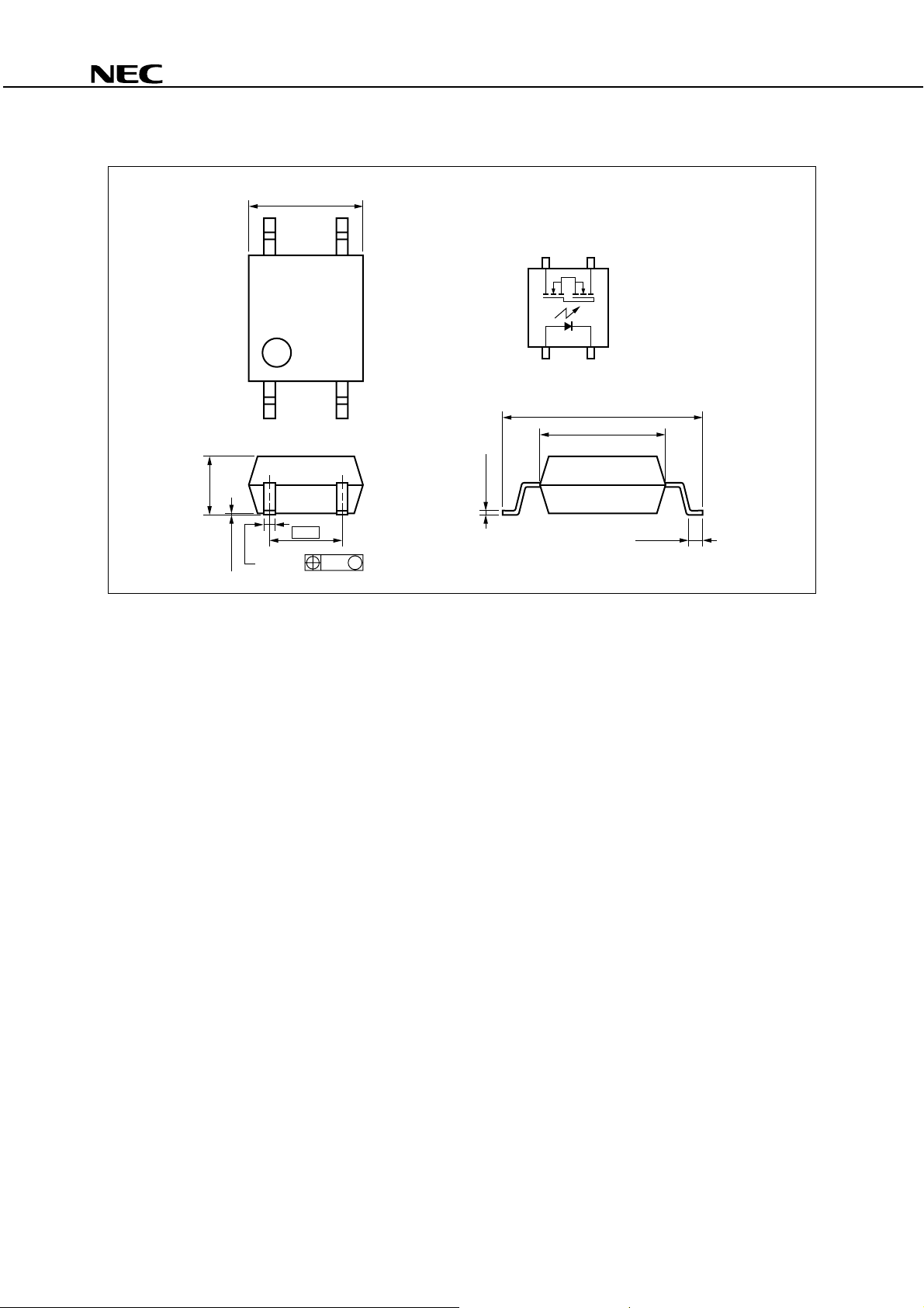
PACKAGE DIMENSIONS (UNIT: mm)
4.0±0.5
–0.05
+0.08
2.05
–0.05
+0.10
0.15
PS7241E-1A
TOP VIEW
43
1. LED Anode
2. LED Cathode
3. MOS FET
4. MOS FET
12
7.0±0.3
4.4
–0.05
+0.08
0.05
0.40
+0.10
–0.05
2.54
0.25 M
0.5±0.3
2
Preliminary Data Sheet PN10459EJ01V0DS
ORDERING INFORMATION
Part Number Package Packing Style
PS7241E-1A 4-pin SOP Magazine case 100 pcs PS7241E-1A
PS7241E-1A-E3 Embossed Tape 900 pcs/reel
PS7241E-1A-E4
PS7241E-1A-F3 Embossed Tape 3 500 pcs/reel
PS7241E-1A-F4
Application Part Number
*1 For the application of the Safety Standard, following part number should be used.
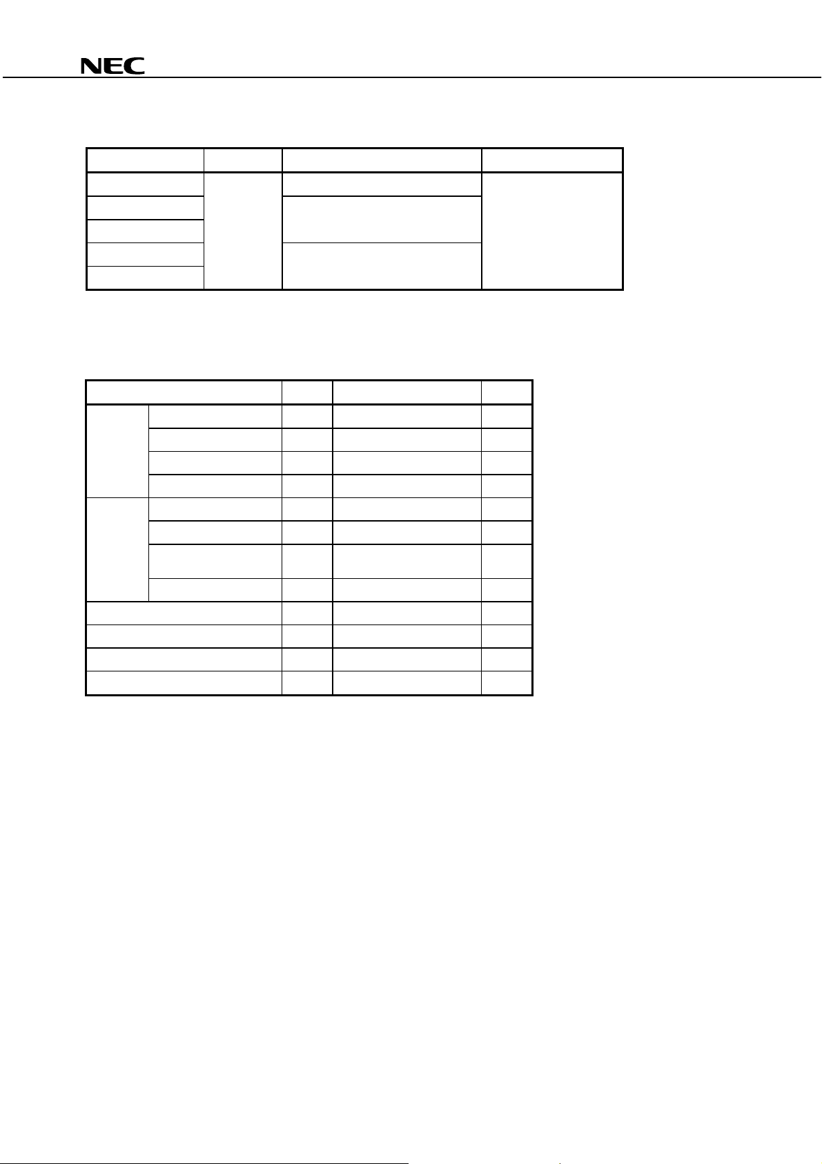
ABSOLUTE MAXIMUM RATINGS (TA = 25°C, unless otherwise specified)
Parameter Symbol Ratings Unit
Diode Forward Current (DC) IF 50 mA
Reverse Voltage VR 5.0 V
Power Dissipation PD 50 mW
Peak Forward Current
MOS FET Break Down Voltage V L 400 V
Continuous Load Current IL 120 mA
Power Dissipation PD 300 mW
Isolation Voltage
Total Power Dissipation PT 350 mW
Operating Ambient Temperature TA −40 to +85 °C
Storage Temperature Tstg −40 to +100 °C
Pulse Load Current
(AC/DC Connection)
*3
BV 1 500 Vr.m.s.
*1 PW = 100
µ
s, Duty Cycle = 1%
*2 PW = 100 ms, 1 shot
*3 AC voltage for 1 minute at T
*1
IFP 1 A
*2
I
LP 240 mA
A = 25°C, RH = 60% between input and output
PS7241E-1A
*1
Preliminary Data Sheet PN10459EJ01V0DS
3

PS7241E-1A
RECOMMENDED OPERATING CONDITIONS (TA = 25°C)
Parameter Symbol MIN. TYP. MAX. Unit
LED Operating Current IF 4 10 20 mA
LED Off Voltage VF 0 0.5 V
ELECTRICAL CHARACTERISTICS (TA = 25°C)
Parameter Symbol Conditions MIN. TYP. MAX. Unit
Diode Forward Voltage VF IF = 10 mA 1.2 1.4 V
Reverse Current IR VR = 5 V 5.0
MOS FET Off-state Leakage
Current
Output Capacitance Cout VD = 0 V, f = 1 MHz 18 pF
Coupled LED On-state Current IFon IL = 120 mA 4.0 mA
On-state Resistance Ron1 IF = 10 mA, IL = 10 mA 22 35
Ron2 IF = 10 mA, IL = 120 mA, t ≤ 10 ms 17 23
Turn-on Time*1 ton IF = 10 mA, VO = 5 V, RL = 500 Ω, 0.5 1.0 ms
Turn-off Time*1 toff PW ≥ 10 ms 0.07 0.2
Isolation Resistance RI-O VI-O = 1.0 kVDC 109
Isolation Capacitance CI-O V = 0 V, f = 1 MHz 0.5 pF
ILoff VD = 400 V 1.0
*1 Test Circuit for Switching Time
µ
A
µ
A
Ω
Ω
I
F
Pulse Input
Input monitor monitorV
R
in
50%
0
90%
10%
Input
VO = 5 V
Output
t
on
t
off
V
L
O
R
L
4
Preliminary Data Sheet PN10459EJ01V0DS

TAPING SPECIFICATIONS (in millimeters)
Outline and Dimensions (Tape)
PS7241E-1A
2.0±0.05
Tape Direction
PS7241E-1A-E3 PS7241E-1A-E4
4.0±0.1
1.55±0.1
8.0±0.1
1.5
+0.1
–0
4.6±0.1
1.75±0.1
5.5±0.05
12.0±0.2
2.9 MAX.
7.4±0.1
2.4±0.1
0.3
Outline and Dimensions (Reel)
2.0±0.5
13.0±0.2
φ
R 1.0
Packing: 900 pcs/reel
21.0±0.8
φ
+0
–1.5
180
φ
2.0±0.5
–0
+1
60
φ
13.5±1.0
17.5±1.0
11.9 to 15.4
Outer edge of
flange
Preliminary Data Sheet PN10459EJ01V0DS
5

Outline and Dimensions (Tape)
PS7241E-1A
2.0±0.05
4.0±0.1
1.55±0.1
Tape Direction
PS7241E-1A-F3
8.0±0.1
1.5
+0.1
–0
4.6±0.1
1.75±0.1
5.5±0.05
12.0±0.2
2.9 MAX.
7.4±0.1
2.4±0.1
0.3
PS7241E-1A-F4
Outline and Dimensions (Reel)
2.0±0.5
2.0±0.5
13.0±0.2
φ
330±2.0
φ
100±1.0
R 1.0
21.0±0.8
φ
Packing: 3 500 pcs/reel
φ
13.0±0.2
φ
13.5±1.0
17.5±1.0
11.9 to 15.4
Outer edge of
flange
6
Preliminary Data Sheet PN10459EJ01V0DS

PS7241E-1A
RECOMMENDED SOLDERING CONDITIONS
(1) Infrared reflow soldering
• Peak reflow temperature 260°C or below (package surface temperature)
• Time of peak reflow temperature 10 seconds or less
• Time of temperature higher than 220°C 60 seconds or less
• Time to preheat temperature from 120 to 180°C 120±30 s
• Number of reflows Three
• Flux Rosin flux containing small amount of chlorine (The flux with a
maximum chlorine content of 0.2 Wt% is recommended.)
Recommended Temperature Profile of Infrared Reflow
(heating)
to 10 s
260˚C MAX.
220˚C
to 60 s
180˚C
120˚C
Package Surface Temperature T (˚C)
120±30 s
(preheating)
Time (s)
(2) Wave soldering
• Temperature 260°C or below (molten solder temperature)
• Time 10 seconds or less
• Preheating conditions 120°C or below (package surface temperature)
• Number of times One
• Flux Rosin flux containing small amount of chlorine (The flux with a maximum chlorine
content of 0.2 Wt% is recommended.)
(3) Cautions
• Fluxes
Avoid removing the residual flux with freon-based and chlorine-based cleaning solvent.
Preliminary Data Sheet PN10459EJ01V0DS
7

PS7241E-1A
•
The information in this document is current as of January, 2004. The information is subject to
change without notice. For actual design-in, refer to the latest publications of NEC's data sheets or
data books, etc., for the most up-to-date specifications of NEC semiconductor products. Not all
products and/or types are available in every country. Please check with an NEC sales representative
for availability and additional information.
•
No part of this document may be copied or reproduced in any form or by any means without prior
written consent of NEC. NEC assumes no responsibility for any errors that may appear in this document.
•
NEC does not assume any liability for infringement of patents, copyrights or other intellectual property rights of
third parties by or arising from the use of NEC semiconductor products listed in this document or any other
liability arising from the use of such products. No license, express, implied or otherwise, is granted under any
patents, copyrights or other intellectual property rights of NEC or others.
•
Descriptions of circuits, software and other related information in this document are provided for illustrative
purposes in semiconductor product operation and application examples. The incorporation of these
circuits, software and information in the design of customer's equipment shall be done under the full
responsibility of customer. NEC assumes no responsibility for any losses incurred by customers or third
parties arising from the use of these circuits, software and information.
•
While NEC endeavours to enhance the quality, reliability and safety of NEC semiconductor products, customers
agree and acknowledge that the possibility of defects thereof cannot be eliminated entirely. To minimize
risks of damage to property or injury (including death) to persons arising from defects in NEC
semiconductor products, customers must incorporate sufficient safety measures in their design, such as
redundancy, fire-containment, and anti-failure features.
•
NEC semiconductor products are classified into the following three quality grades:
"Standard", "Special" and "Specific". The "Specific" quality grade applies only to semiconductor products
developed based on a customer-designated "quality assurance program" for a specific application. The
recommended applications of a semiconductor product depend on its quality grade, as indicated below.
Customers must check the quality grade of each semiconductor product before using it in a particular
application.
"Standard": Computers, office equipment, communications equipment, test and measurement equipment, audio
and visual equipment, home electronic appliances, machine tools, personal electronic equipment
and industrial robots
"Special": Transportation equipment (automobiles, trains, ships, etc.), traffic control systems, anti-disaster
systems, anti-crime systems, safety equipment and medical equipment (not specifically designed
for life support)
"Specific": Aircraft, aerospace equipment, submersible repeaters, nuclear reactor control systems, life
support systems and medical equipment for life support, etc.
The quality grade of NEC semiconductor products is "Standard" unless otherwise expressly specified in NEC's
data sheets or data books, etc. If customers wish to use NEC semiconductor products in applications not
intended by NEC, they must contact an NEC sales representative in advance to determine NEC's willingness
to support a given application.
(Note)
(1) "NEC" as used in this statement means NEC Corporation, NEC Compound Semiconductor Devices, Ltd.
and also includes its majority-owned subsidiaries.
(2) "NEC semiconductor products" means any semiconductor product developed or manufactured by or for
NEC (as defined above).
M8E 00. 4 - 0110
8
Preliminary Data Sheet PN10459EJ01V0DS

PS7241E-1A
Caution GaAs Products
This product uses gallium arsenide (GaAs).
GaAs vapor and powder are hazardous to human health if inhaled or ingested, so please observe
the following points.
• Follow related laws and ordinances when disposing of the product. If there are no applicable laws
and/or ordinances, dispose of the product as recommended below.
1. Commission a disposal company able to (with a license to) collect, transport and dispose of
materials that contain arsenic and other such industrial waste materials.
2. Exclude the product from general industrial waste and household garbage, and ensure that the
product is controlled (as industrial waste subject to special control) up until final disposal.
• Do not burn, destroy, cut, crush, or chemically dissolve the product.
• Do not lick the product or in any way allow it to enter the mouth.
For further information, please contact
NEC Compound Semiconductor Devices, Ltd. http://www.ncsd.necel.com/
E-mail: salesinfo@ml.ncsd.necel.com (sales and general)
techinfo@ml.ncsd.necel.com (technical)
5th Sales Group, Sales Division TEL: +81-44-435-1588 FAX: +81-44-435-1579
NEC Compound Semiconductor Devices Hong Kong Limited
E-mail: ncsd-hk@elhk.nec.com.hk (sales, technical and general)
Hong Kong Head Office
Taipei Branch Office
Korea Branch Office
NEC Electronics (Europe) GmbH http://www.ee.nec.de/
TEL: +49-211-6503-01 FAX: +49-211-6503-487
California Eastern Laboratories, Inc. http://www.cel.com/
TEL: +1-408-988-3500 FAX: +1-408-988-0279
TEL: +852-3107-7303
TEL: +886-2-8712-0478
TEL: +82-2-558-2120
FAX: +852-3107-7309
FAX: +886-2-2545-3859
FAX: +82-2-558-5209
0310
 Loading...