

NEC NEC-FA150ATUA Service Manual

Service Manual
15-inch LCD Monitor
NEC-FA150ATUA

Service Manual Versions and Revision
No. Version Release Date Revision
1. 1.0 October 2, 2001 Original release
2 1.1 October 11, 2001 Circuit Description
9 (3) -- page 7
Trouble Shooting
4 -- page 6
6 -- page 8
14.3 -- page 20
3 1.2 October 16, 2001 Circuit Description
1.1 -- page 1
5 -- page 3
9.2.1 (2) -- page 6
9.2.1 (3) -- page 7
9.4.1 -- page 8
Trouble Shooting
3 -- page 5
13 -- page 17
Copyright
Copyright 2001 LiteOn Technology Corp.
All Rights Reserved
This manual may not, in whole or in part, be
copied, photocopied, reproduced, translated, or
converted to any electronic or machine readable
form without prior written permission of LiteOn
Technology Corp.
NEC FA150ATUA Service Manual.
Printed in Taiwan.
Trademarks
LiteOn is a registered trademark of LiteOn
Technology Corp.
All other trademarks are the property of their
respective owners.

Table of Contents
1. Audio circuit --------------------------------------------------------------------------------------------------------------- 1
1.1 Audio input ------------------------------------------------------------------------------------------------------------ 1
1.2 Audio output ---------------------------------------------------------------------------------------------------------- 1
2. Power supply -------------------------------------------------------------------------------------------------------------- 1
3. On-screen circuit ---------------------------------------------------------------------------------------------------------- 2
4. Video input circuit -------------------------------------------------------------------------------------------------------- 3
5. Definition converter LSI peripheral circuit ---------------------------------------------------------------------------- 3
6. System reset, LED control circuit --------------------------------------------------------------------------------------- 4
7. E2PROM for PNP --------------------------------------------------------------------------------------------------------- 5
8. E2PROM -------------------------------------------------------------------------------------------------------------------- 6
9. CPU circuit ----------------------------------------------------------------------------------------------------------------- 6
9.1 Dection of POWER switch status ---------------------------------------------------------------------------------- 6
9.2 Display mode identification ----------------------------------------------------------------------------------------- 6
9.3 User control ----------------------------------------------------------------------------------------------------------- 8
9.4 Control of identification converter MCU I306 ------------------------------------------------------------------- 8
9.5 I2C bus control -------------------------------------------------------------------------------------------------------- 9
9.6 Power ON sequence -------------------------------------------------------------------------------------------------10
9.7 Power OFF sequence ------------------------------------------------------------------------------------------------ 11
9.8 List of CPU Pin Assignments -------------------------------------------------------------------------------------- 12
10. Inverter -------------------------------------------------------------------------------------------------------------------- 15
11. USB circuit ---------------------------------------------------------------------------------------------------------------- 18
Circuit Description

NEC-FA150ATUA
1. Audio circuit (Circuit diagrams Main PWB) KT
1.1 Audio input
The audio signal input received from the audio input terminal (J301) is applied to the amplifier I314 of 4 (L-CH)
and 9 (R-CH) through the low-pass filter consisting of R374, R376, R378, R379, C464 and C465.
In this amplifier, controls of Volume, and mute are conducted. The audio signal controlled at the pin 6 deter-
mines the attenuation of output of the amplifiers. Since then, the signal is output to the jack P307.
1.2 Audio output
The audio signal is output from the jack output terminal (P307) of the jack board to the internal speaker system.
2. Power supply (Circuit daigrams MAIN PWB)
1. Line filter consists of C801, T801, C803, C804. It eliminates high frequency interference to meet EMIs
requirement.
2. Rec & Filter
Bridge diode D801 converts AC source into pulsed DC. This pulsed DC is smoothed and filtered by C805.
R802 is an NTC ( negative thermal coefficient ) resistor, used to reduce inrush current to be within safe range.
3. Power transformer :
T802 converts energy from power source C805 to secondary side to generate +12V and +5V.
4. Output :
When driver Q803 is driven on and off by I801, pin 6 and pin 9 of T802 induce a square wave. This square
wave is rectified by D809, D810, then filtered by C817, C822 to generate +12V and +5V respectively.
5. Driver : Q803
If the electrical potential of gate is larger than source by about 10 volts, Q803 turns on.
6. FB :
Negative feedback CKT consists of photo coupler I802 and adjustable regulator I803. It can maintain output
voltages +5V and +12V at a stable level.
7. PWM :
7.17.1
StartStart
7.1
7.17.1
7.27.2
7.2
7.27.2
: When power is turned on, Q801 conducts due to bias from C805 and R803. Q801 supplies a 17 volt : When power is turned on, Q801 conducts due to bias from C805 and R803. Q801 supplies a 17 volt
Start
: When power is turned on, Q801 conducts due to bias from C805 and R803. Q801 supplies a 17 volt
StartStart
: When power is turned on, Q801 conducts due to bias from C805 and R803. Q801 supplies a 17 volt : When power is turned on, Q801 conducts due to bias from C805 and R803. Q801 supplies a 17 volt
and a starting current about 0.3mA to pin 7 of I801. I801 starts to oscillate (R816, C813) and outputs a pulseand a starting current about 0.3mA to pin 7 of I801. I801 starts to oscillate (R816, C813) and outputs a pulse
and a starting current about 0.3mA to pin 7 of I801. I801 starts to oscillate (R816, C813) and outputs a pulse
and a starting current about 0.3mA to pin 7 of I801. I801 starts to oscillate (R816, C813) and outputs a pulseand a starting current about 0.3mA to pin 7 of I801. I801 starts to oscillate (R816, C813) and outputs a pulse
train through pin 6 to drive Q803.train through pin 6 to drive Q803.
train through pin 6 to drive Q803.
train through pin 6 to drive Q803.train through pin 6 to drive Q803.
OPPOPP
: When Q803 turns on, C805 supplies a linearly increasing triangle current through the primary induc- : When Q803 turns on, C805 supplies a linearly increasing triangle current through the primary induc-
OPP
: When Q803 turns on, C805 supplies a linearly increasing triangle current through the primary induc-
OPPOPP
: When Q803 turns on, C805 supplies a linearly increasing triangle current through the primary induc- : When Q803 turns on, C805 supplies a linearly increasing triangle current through the primary induc-
tance of T802 to the driver Q803, once the peak value of this current multiplied by R81tance of T802 to the driver Q803, once the peak value of this current multiplied by R81
tance of T802 to the driver Q803, once the peak value of this current multiplied by R81
tance of T802 to the driver Q803, once the peak value of this current multiplied by R81tance of T802 to the driver Q803, once the peak value of this current multiplied by R81
train will be shut down immediately to protect Q803, T802 from being burned out.train will be shut down immediately to protect Q803, T802 from being burned out.
train will be shut down immediately to protect Q803, T802 from being burned out.
train will be shut down immediately to protect Q803, T802 from being burned out.train will be shut down immediately to protect Q803, T802 from being burned out.
1 exceeds1 volt, pulse1 exceeds1 volt, pulse
1 exceeds1 volt, pulse
1 exceeds1 volt, pulse1 exceeds1 volt, pulse
7.37.3
RegulationRegulation
7.3
Regulation
7.37.3
RegulationRegulation
tor and photo diode flows more current. The voltage of pin 2 goes up too, making the pulse width of pin 6 totor and photo diode flows more current. The voltage of pin 2 goes up too, making the pulse width of pin 6 to
tor and photo diode flows more current. The voltage of pin 2 goes up too, making the pulse width of pin 6 to
tor and photo diode flows more current. The voltage of pin 2 goes up too, making the pulse width of pin 6 totor and photo diode flows more current. The voltage of pin 2 goes up too, making the pulse width of pin 6 to
become narrower. So the output voltage +5V will be pulled down to a stable value.become narrower. So the output voltage +5V will be pulled down to a stable value.
become narrower. So the output voltage +5V will be pulled down to a stable value.
become narrower. So the output voltage +5V will be pulled down to a stable value.become narrower. So the output voltage +5V will be pulled down to a stable value.
: If output voltage +5V goes up, the R terminal of I803 gets more bias, accordingly photo transis- : If output voltage +5V goes up, the R terminal of I803 gets more bias, accordingly photo transis-
: If output voltage +5V goes up, the R terminal of I803 gets more bias, accordingly photo transis-
: If output voltage +5V goes up, the R terminal of I803 gets more bias, accordingly photo transis- : If output voltage +5V goes up, the R terminal of I803 gets more bias, accordingly photo transis-
Page 1Circuit Description
NEC-FA150ATUA
7.47.4
OVPOVP
7.4
7.47.4
7.57.5
7.5
7.57.5
: If +5V goes up too much, the induced voltage on pin 4 of T802 becomes lar : If +5V goes up too much, the induced voltage on pin 4 of T802 becomes lar
OVP
: If +5V goes up too much, the induced voltage on pin 4 of T802 becomes lar
OVPOVP
: If +5V goes up too much, the induced voltage on pin 4 of T802 becomes lar : If +5V goes up too much, the induced voltage on pin 4 of T802 becomes lar
over 22 volts, ZD803 conducts, Q806 is triggered on, pin 1 of I801 is pulled down to ground, the pulse trainover 22 volts, ZD803 conducts, Q806 is triggered on, pin 1 of I801 is pulled down to ground, the pulse train
over 22 volts, ZD803 conducts, Q806 is triggered on, pin 1 of I801 is pulled down to ground, the pulse train
over 22 volts, ZD803 conducts, Q806 is triggered on, pin 1 of I801 is pulled down to ground, the pulse trainover 22 volts, ZD803 conducts, Q806 is triggered on, pin 1 of I801 is pulled down to ground, the pulse train
at pin 6 goes down to zero, shutting Q803 ofat pin 6 goes down to zero, shutting Q803 of
at pin 6 goes down to zero, shutting Q803 of
at pin 6 goes down to zero, shutting Q803 ofat pin 6 goes down to zero, shutting Q803 of
SCPSCP
: If output terminal is short to ground, photo transistor does not conduct, hence Q805 does not conduct : If output terminal is short to ground, photo transistor does not conduct, hence Q805 does not conduct
SCP
: If output terminal is short to ground, photo transistor does not conduct, hence Q805 does not conduct
SCPSCP
: If output terminal is short to ground, photo transistor does not conduct, hence Q805 does not conduct : If output terminal is short to ground, photo transistor does not conduct, hence Q805 does not conduct
neitherneither
. The reference voltage +5V at pin 8 begins to char. The reference voltage +5V at pin 8 begins to char
neither
. The reference voltage +5V at pin 8 begins to char
neitherneither
. The reference voltage +5V at pin 8 begins to char. The reference voltage +5V at pin 8 begins to char
pin 1 down to ground, shutting Q803 ofpin 1 down to ground, shutting Q803 of
pin 1 down to ground, shutting Q803 of
pin 1 down to ground, shutting Q803 ofpin 1 down to ground, shutting Q803 of
LCD 1550M Power Board Block Diagram
f completelyf completely
f completely
f completelyf completely
f completelyf completely
f completely
f completelyf completely
..
.
..
ge on C829 and activates Q806 to conduct, pullingge on C829 and activates Q806 to conduct, pulling
ge on C829 and activates Q806 to conduct, pulling
ge on C829 and activates Q806 to conduct, pullingge on C829 and activates Q806 to conduct, pulling
..
.
..
ge also. Suppose that it isge also. Suppose that it is
ge also. Suppose that it is
ge also. Suppose that it isge also. Suppose that it is
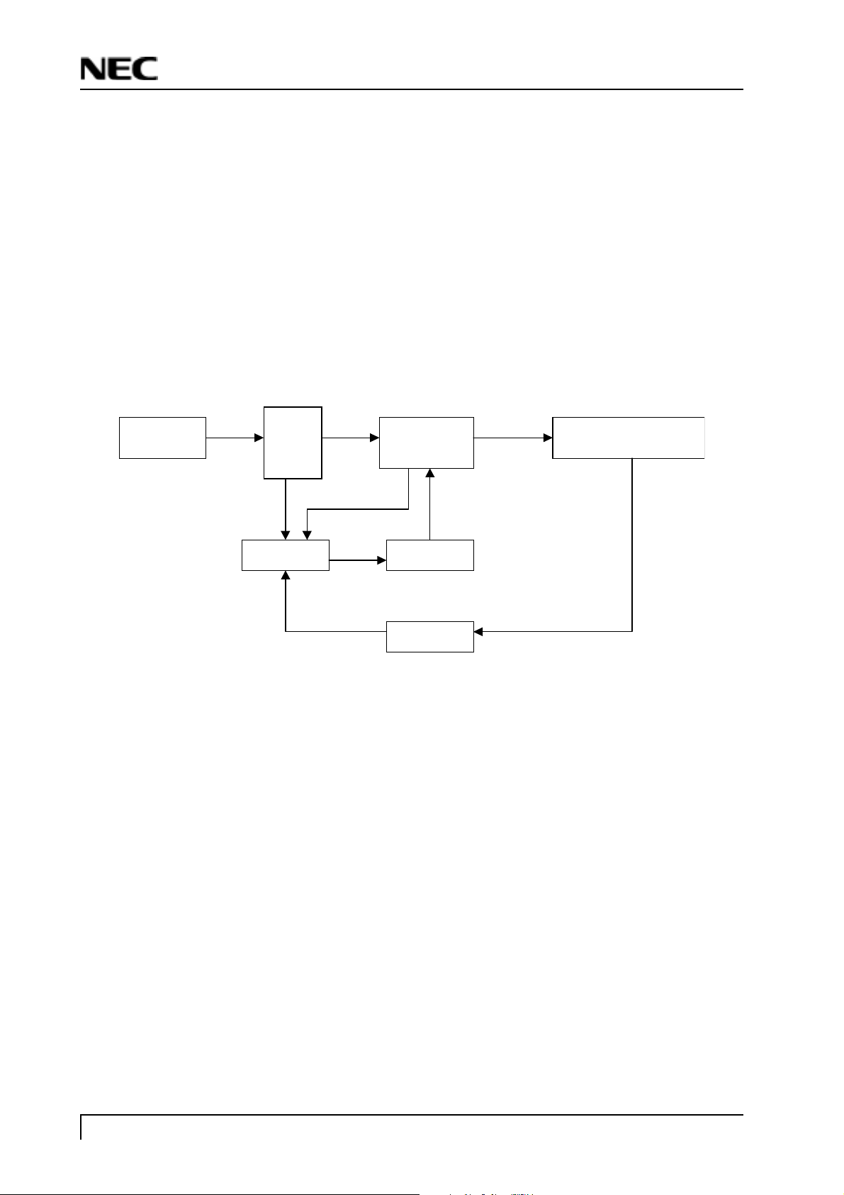
Line Filter
Rec.
&
Filter
PWM Driver
Power
Transformer
FB
Output Rec. & Filter
3. On-screen circuit (Circuit diagrams Main PWB 3/6)
I305 (M66611) Embeded function.
OSD (character pattern display controller) is a module by which the character data beforehand prepared on the normal
display data is inserted (display) in an arbitrary position. SRAM can be built into internally for the character storage
and it is possible to compose the flexible data of the user side.
The outline is shown in Table 1.1.
Page 2 Circuit Description
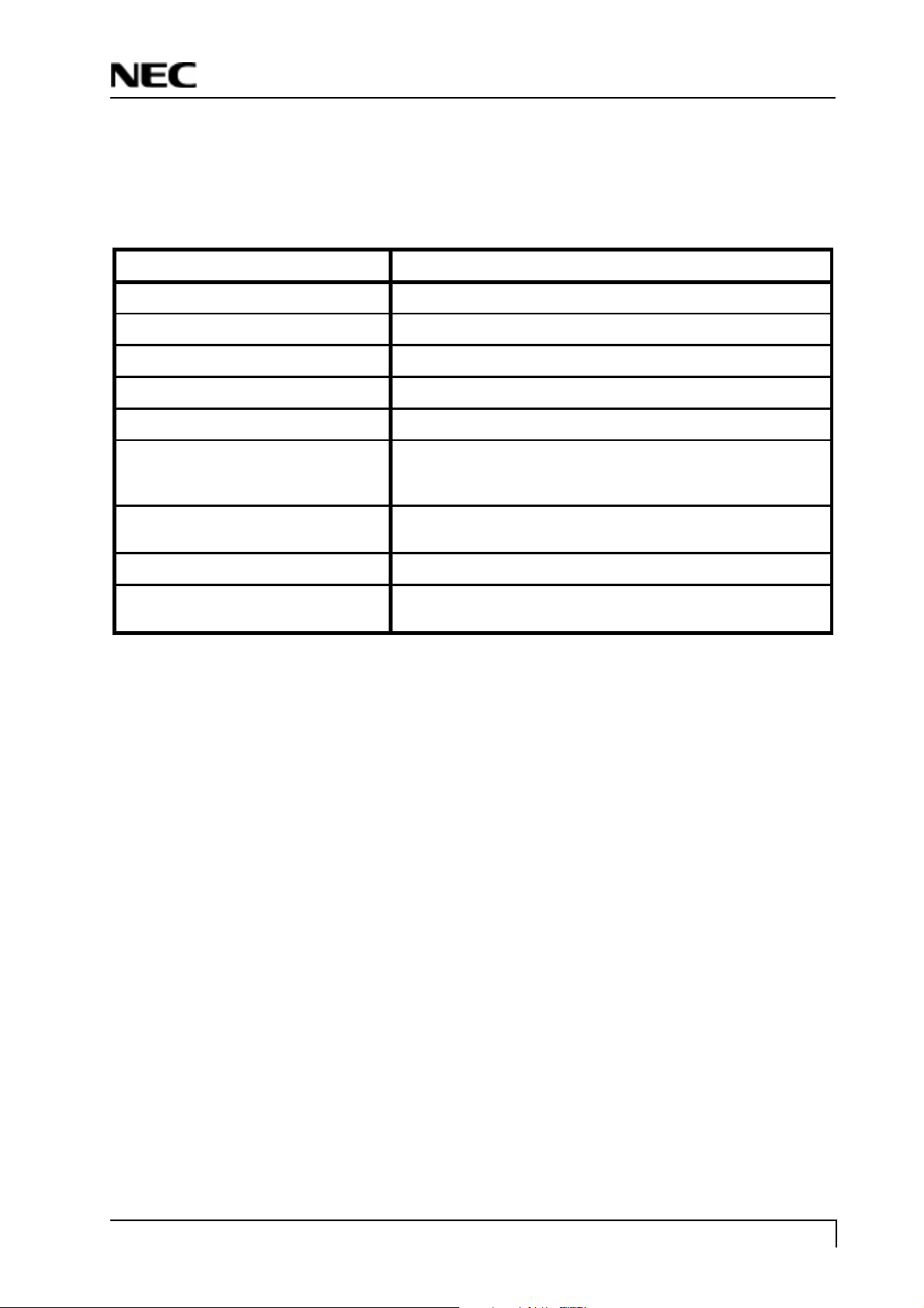
Table 1.1 Outline for OSD
Item Outline
Screen Composition 24 digits x 12 lines x 1 page
Number of display characters Max. 288 characters
Character composition 12 x 180 dots
Kind of character 64 kinds
Character size 4 (Ver. Direction) x 2 kind (Hor. Direction)
Character unit
Blinking
(32/64 viding frequency of vertical synchronization, duty: 25, 50
and 75%)
NEC-FA150ATUA
Coloring
Blanking Character size / Border size / Matrix-outline size / All blanking
Function of deletion of batch of display
RAM
Character color (character unit)/
Character background color (character unit)
Built-in (field memory)
4. Video input circuit (Circuit diagram MAIN PWB 2/6)
RAIN Analog Input for RED Channel
GAIN Analog Input for GREEN Channel
BAIN Analog Input for BLUE Channel
High-impedance inputs that accept the RED, GREEN, and BLUE channel graphics signals, respectively. (The three
channels are identical, and can be used for any colors, but colors are assigned for convenient reference.)
They accommodate input signals ranging from 0.5V to 1.0V full scale. Signals should be ac-coupled to these pins to
support clamp operation.
5. Definition converter LSI peripheral circuit (Circuit diagram MAIN PWB)
I305 M66611FP is the definition converter LSI.
DESCRIPTION
M66611FP Series is a picture processor for the flat panel displays, it have unique picture processing function that high
quality picture scaling and color coversion with keeping white balance. Low cost chip-set solution is provided.
FEATURES
l Input and output format compatibility:
-16.7 million colors in all formats
-VGA to SXGA inputs
-SXGA output (Available for B grade ver.)
Page 3Circuit Description

NEC-FA150ATUA
l Input port:
-Up to 135 Mpixels/sec (Available for B grade ver.)
-24/48-bit RGB programmable, (one or two pixel-per-clock respectively)
-Seperate / composite syncs
-Glue-less interface to analog front end ICs
-TMDS receiver interface
-Interface to NTSC-digital decode ICs (YUV to RGB conversion, simplified inter less processing.)
lDisplay port:
-Up to 135 Mpixels/sec (by 48bit RGB port/B grade ver.)
-24/48-bit RGB programmable. (one or two pixel-per-clock LCD panel respectively)
-Supports 18-bit and 24-bit display
-Programmable timing generator
l PICT clock rate conversion:
-50Hz to 75Hz input refresh rates for VGA to SXGA
-50Hz to 75Hz output refresh rate (must be the same as input rate)
-No extermal frame memory required
l Programmable picture processing:
-High quality picture scaling
-Up/down scaling from VGA, SVGA, XGA, or SXGA to XGA
-Indenpendent horizontal and vertical scaling
-Edge enhancement / smoothing (M66611)
-Color conversion with keeping white balance (M66611)
-Color space expanding to 24-bit full color for 18-bit LCD panel
-1024-extry gamma table for each R,G, B color (M66611)
6. System reset, LED control circuit (Circuit diagram MAIN PWB 4/6)
6.1 System reset
System reset is performed by detecting the rising and falling of the 3.3V source voltage at I309.
There are two kinds of resets;hardware and software. In both cases, operation is the same after the reset. (See Software
Reset for details of software resets.) This section explains on hardware resets.
When the supply voltage is in the range where operation is guaranteed, a reset is effected by holding the reset pin level
L (0.2Vcc max.) for at least 20 cycles. When the reset pin level is then returned to the H level while main clock is
stable, the reset status is cancelled and program execution resumes from the address in the reset vector table.
Figure 6.1 showns the example reset circuit. Figure 6.2 shows the reset sequence.
6.2 LED control circuit
Green / amber is lit with the control signal of the LED GREEN and LED AMBER signal pin 66, 65 from I306 (Circuit
diagram MAIN PWB 4/6).
Page 4 Circuit Description
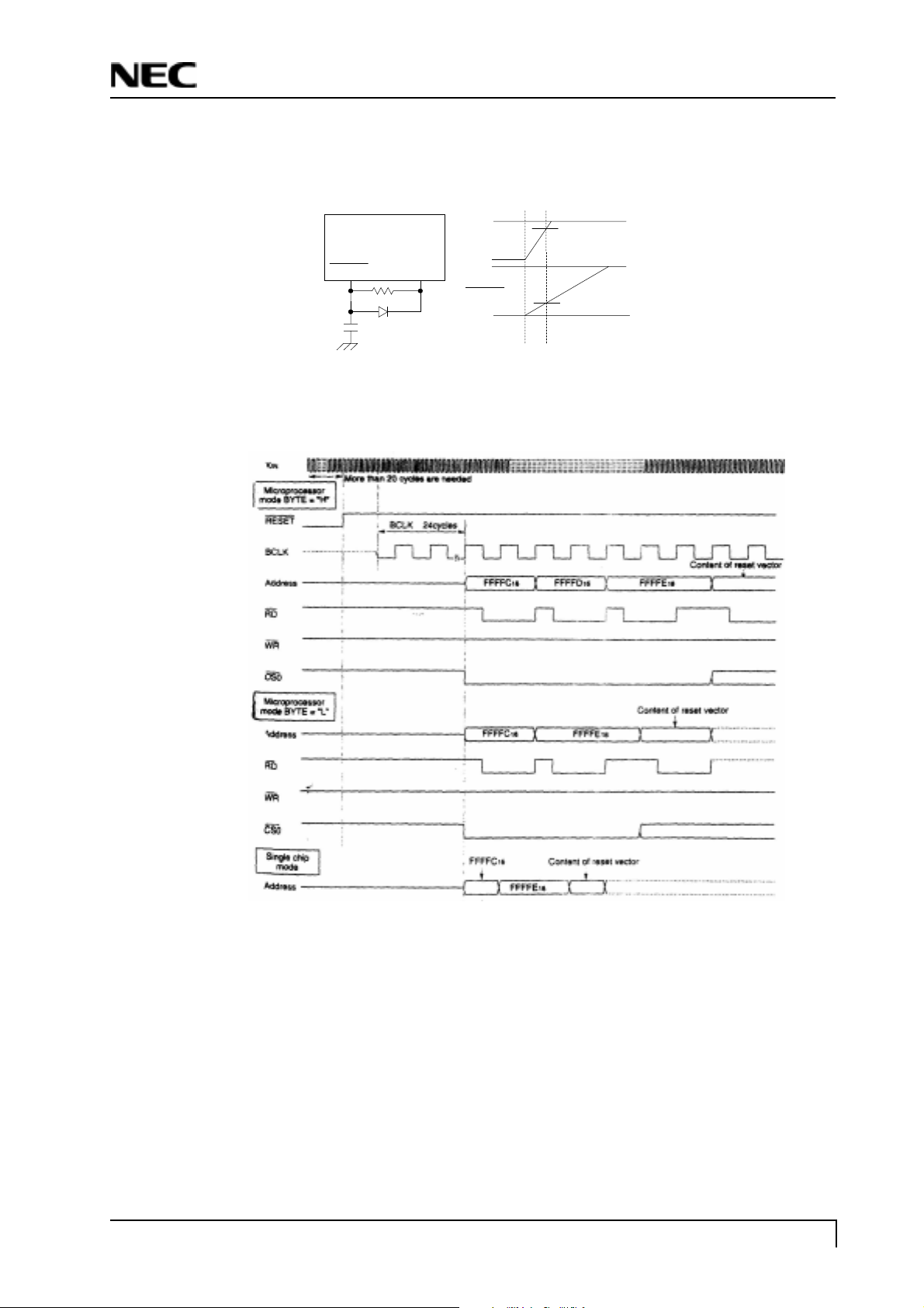
Figure 6.1 Example reset circuit
NEC-FA150ATUA
Figure 6.2 RESET sequence
RESET Vcc
Example when Vcc=3.3V
3.3V
Vcc
0V
5V
RESET
0V
2.75V
0.8V
7. E2PROM for PnP (Circuit diagram MAIN PWB)
Data transfer between I304 and host.
There are two forms of communications protocal. In both, display capabilities are retrieved by the system software
during the boot-up and configuration time.
For the PC platform, this software layer is defined in the VESA BIOS Extension / Display Data Channel, VBE/DDC,
standard.
Page 5Circuit Description

NEC-FA150ATUA
8. E2PROM (Circuit diagram MAIN PWB 4/6)
Data transfer between I308 (24LC32) and CPU (I306) is effected through the IIC bus SCL (pin 80) and SDA (pin
81) of I306. The data to be transferred to each device are stored in I308.
l I303 control data.
9. CPU circuit (Circuit diagram MAIN PWB 4/6)
I306 (M30620FGMGP) functions as the CPU.
The source voltage for the device is 3.3V and the system clock frequency is 10MHz.
9.1 Detection of POWER switch status
The CPU identifies the ON status of the two power supplies. The identification is made when the power supply
is turned off. For example, if the power supply is turned off with the POWER switch, the POWER switch must be
turned on when activating the power supply again. If the power supply is turned off by pulling out the power
cord, then this power supply can be turned on by connecting the power cord, without pressing the POWER
switch.
9.2 Display mode identification
9.2.1 Functions
(1) Display mode identification
l The display mode of input signal is identified based on Table 1, and according to the frequency and polarity
(HPOL, VPOL) of horizontal or vertical sync signal, presence of the horizontal or vertical sync signal, and the
discrimination signal (HSYNC_DETECT, VSYNC_DETECT).
l When the mode has been identified through the measurement of horizontal and vertical frequencies, the total
number of lines is determined with a formula of Horizontal frequency / Vertical frequency = Total number
of lines. Final identification can be made by examining the coincidence of the obtained figure with the
number of lines for the mode identified from the frequency.
l When the detected frequency if the sync signal has changed, the total number of lines should be counted even
through it identified frequency in the same mode. Then, it is necessary to examine whether the preset value for
the vertical display position has exceeded the total number of lines. If exceeded, a maximum value should be
set up.
(2) Power save mode.
The power save mode is assumed when the horizontal / vertical signals are as specified below.
l If there is no horizontal sync signal input or below 10KHz.
l If there is no vertical sync signal input or below 10Hz.
Page 6 Circuit Description

Table 1 Preset Timing Chart
NEC-FA150ATUA
Preset Resolution
0 Non-interlaced PAL* 31.25 27 - -
1 VGA 720 x 350 70Hz 31.47 28.322 + -
2 PC98 640 x 400 56Hz * 24.83 21.053 +/- +/-
3 VGA 720 x 400 70Hz 31.47 28.322 - +
4 VGA 640 x 480 60Hz 31.47 25.175 +/- +/-
5 MAC 640 x 480 66Hz 35 30.24 +/- +/-
6 VESA 640 x 480 72Hz 37.86 31.5 +/- +/-
7 VESA 640 x 480 75Hz 37.5 31.5 - -
8 VESA 800 x 600 56Hz 35.16 36 +/- +/-
9 VESA 800 x 600 60Hz 37.88 40 +/- +/-
10 VESA 800 x 600 75Hz 46.88 49.5 +/- +/-
11 VESA 800 x 600 72Hz 48.08 50 +/- +/-
H-freq
(KHz)
Band Width
(MHz)
Polarity
HV
12 MAC 832 x 624 75Hz 49.72 57.283 +/- +/-
13 VESA 1024 x 768 60Hz 48.36 65 +/- +/-
14 SUN 1024 x 768 65Hz 52.45 70.49 +/- +/-
15 VESA 1024 x 768 70Hz 56.48 75 +/- +/-
16 VESA 1024 x 768 75Hz 60.02 78.75 +/- +/-
(3) Out of range
When resolution beyond 1024 x 768 is inputted, resolution is lowered with Down scaling to 1024 x 768, and
indicated, and OSD should indicate OUT of Range.
l If the horizontal sync signal is outside the measuring range 31.5KHz - 60KHz
l If the vertical syna signal is outside the measuring range 56.2Hz - 75.1Hz
Page 7Circuit Description
NEC-FA150ATUA
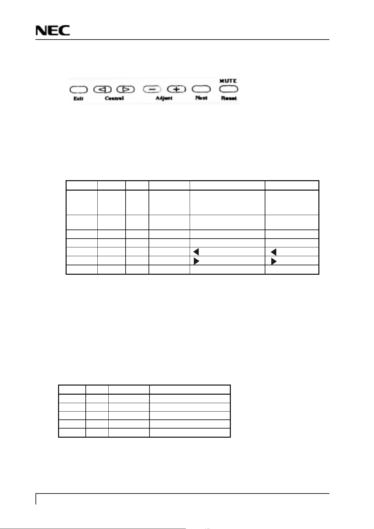
9.3 User Control
General Key Description
Exit: Turn off OSM menu, Exit sub menu.
Control: Move the green cursor amd select control items.
Adjust: Change the value of each function / Enter to submenu / Proceed auto adjust / Proceed reset
Next: Move the NEXT tag
Reset: Reset the select item (Open reset warning before reset) / Mute the speaker / headphone sound (short cut: when
no OSM menu is shown)
9.3.1 Related ports of I306
Port Pin No. I/O Signal name Function Remarks
P3.5 55 1 RESET /
Mute
P3.1 59 1 EXIT EXIT switch input Withdraw from
P3.4 56 1 DOWN - switch input ( - ) key
P3.3 57 1 UP + switch input ( + ) key
P3.2 58 1 LEFT switch input ( ) key
P3.6 54 1 RIGHT switch input ( ) key
P3.7 53 1 NEXT NEXT switch input
RESET switch input
MUTE switch input
The set value is
returned to the
initial value
OSD
9.3.2 Functions
Control is effected for the push-switches to be used when the user changes the parameters, in order to modify the
respective setting values. Whether the switch has been pressed is identified with the switch input level that is
turned L.
Each switch input port is pulled up at outside of MCU.
Each parameter is stored in the EEPROM, the contents of which are updated as required.
9.4 Control of definition converter MCU I306.
9.4.1 Ports related to control
Pin No. I/O Signal name Function
33 O SSI Serial data Input to M66611
34 I SSO Serial data Output to M66611
35 O SCK Serial clock Input to M66611
36 O SCSB Chip select to M66611
37 I SRDYB Ready output
Page 8 Circuit Description
9.4.2 Functions
Major function of I305 are as follows:
(1) Expansion of the display screen.
(2) Timing control for various signal types.
(3) Power-supply sequence (LCD panel).
9.5 I2C bus control
9.5.1 Related ports of I306
Port Pin No. I/O Signal name Function
P0.6 80 I IICCLK IIC bus clock
P0.5 81 I/O IICDATA IIC bus data
9.5.2 I2C-controlled functions
The following functional controls are effected by I2C.
(1) Control of EEPROM I308f for parameter setting.
(2) Control of audio preamplifier.
NEC-FA150ATUA
Page 9Circuit Description
NEC-FA150ATUA
9.6 Power ON sequence
When the POWER switch is pressed, the POWER OFF signal is turned H. When this H potential is detected,
the CPU begins to establish the respective power supplies according to the sequence shown below.
uP POWER
Panel_VCTL
Panel_CLK
BLON
LED
Panel Data
Page 10 Circuit Description
NEC-FA150ATUA
9.7 Power OFF sequence
When the POWER switch is pressed while the power supply is ON, the POWER ON signal is turned H. When
tshown below.his H potential is detected, the CPU begins to turn off the respective power supplies according
to the sequence
uP Power
Panel-VCTL
Panel-CLK
BLON
LED
Panel Data
Page 11Circuit Description
NEC-FA150ATUA
9.8 List of CPU Pin Assignments
Port Pin No Signal Name Initial SeetingFunction Remark
P9.4
P9.3
P9.2
P9.1
P9.0
P8.7
P8.6
P8.5
P8.4
P8.3
P8.2
P8.1
P8.0
P7.7
P7.6
P7.5
P7.4
P7.3
P7.2
P7.1
P7.0
P6.7
P6.6
P6.5
P6.4
P6.3
P6.2
P6.1
1
Bright ~ Inverter Luminance Control
2
Vo l u m e ~ A u d i o Vo l u me C on t r ol
3
Nc ~ ~
4
Nc ~ ~
5
Nc ~ ~
6
Byte ~ ISP Byte Function
7
CNVss ~ Switches change between processor mode
8
Nc ~ ~
9
Nc ~ ~
10
Reset L Reset Signal at Lower Level with 20 Clock Active L
11
Xout ~ uP Clock Output
12
Vss ~ GND
13
Xin ~ uP Clock Input
14
Vcc ~ uP_Vcc 3.3V
15
NMI ~ uP Interrupt generator When Hi to Low
16
Nc ~ ~
17
V1_Detect ~ VS_ASIC
18
Nc ~ ~
19
H1_Detect ~ HS_ASIC
20
NC ~ ~
21
DE_Detec t ~ DDC_GND
22
BLON H Inverter Enable Control
23
Nc ~ ~
24
Nc ~ ~
25
Nc ~ ~
26
Nc ~ ~
27
DDC_SCL ~ uP_DDC_SCL
28
DDC_SDA ~ uP_DDC_SDA
29
TXD ~ ISP TXD
30
RXD ~ ISP RXD
31
SCLK ~ ISP SCLK
32
BUSY ~ ISP BUSY
33
SSI ~ uP_Clock Serial Data Input
34
SSO ~ uP_Clock Serial Data Output
35
SCK ~ uP_Clocled Serial clock Input
Page 12 Circuit Description
 Loading...