NEC NE960R200, NE961R200 Datasheet

PRELIMINARY DATA SHEET
N-CHANNEL GaAs MES FET
NE960R2 SERIES
0.2 W X, Ku-BAND POWER GaAs MES FET
DESCRIPTION
The NE960R2 Series are 0.2 W GaAs MES FETs designed for middle power transmitter applications for X, Kuband microwave communication systems. It is capable of delivering 0.2 watt of output power (CW) with high linear
gain, high efficiency and low distortion and are suitable as driver amplifiers for our X, Ku-band NEZ Series amplifiers
etc. The NE961R200 and the NE960R200 are available in chip form. The NE960R200 has a via hole source
grounding and PHS (Plated Heat Sink) for superior RF performance. The NE960R275 is available in a hermetically
sealed ceramic package. Reliability and performance uniformity are assured by NEC’s stringent quality and control
procedures.
FEATURES
• High Output Power : P
• High Linear Gain : 10.0 dB TYP.
• High Power Added Efficiency: 35 % TYP. @VDS = 9 V, I
o (1 dB)
= +25.0 dBm TYP.
ORDERING INFORMATION
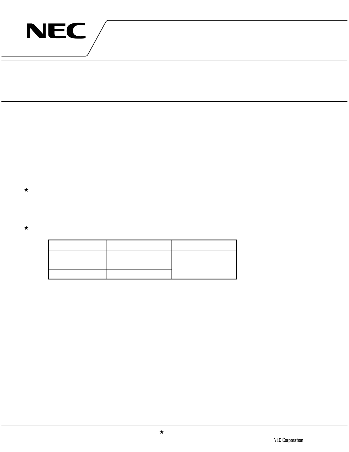
Part Number Package Supplying Form
NE960R200
NE961R200
NE960R275 75
Remark
To order evaluation samples, please contact your local NEC sales office.
(Part number for sample order: NE960R200, NE960R275, NE961R200)
00 (CHIP)
ESD protective envelope
Dset
= 90 mA, f = 14.5 GHz
Caution Please handle this device at static-free workstation, because this is an electrostatic sensitive
device.
The information in this document is subject to change without notice. Before using this document, please
confirm that this is the latest version.
Not all devices/types available in every country. Please check with local NEC representative for
availability and additional information.
Document No. P13775EJ2V0DS00 (2nd edition)
Date Published July 1999 N CP(K)
Printed in Japan
The mark shows major revised points.
1998, 1999©

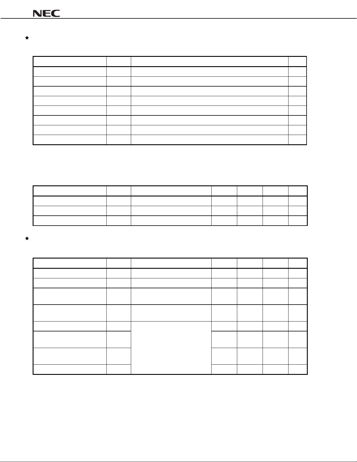
ABSOLUTE MAXIMUM RATINGS (TA = +25°°°°C)
Operation in excess of any one of these parameters may result in permanent damage.
Parameter Symbol Ratings Unit
NE960R2 SERIES
Drain to Source Voltage V
Gate to Source Voltage V
Drain Current I
Gate Forward Current I
Gate Reverse Current I
Total Power Dissipat i on P
Channel Temperature T
Storage Temperature T
NE961R200
Note
DS
GSO
D
GF
GR
T
ch
stg
RECOMMENDED OPERATING CONDITIONS
Parameter Symbol Test Condition MIN. TYP. MAX. Unit
Drain to Source Voltage V
DS
Gain Compression Gcomp
Channel Temperature T
ch
ELECTRICAL CHARACTERISTICS
(TA = +25
°°°°
C, Unless otherwise specified, using NEC standard test fixture.)
15 V
–7 V
0.35 A
+2.5 mA
–2.5 mA
Note
2.5 (2.1
)
175
–65 to +175
−
−−
−−
9.0 9.0 V
3.0 dB
+130
W
°
C
°
C
°
C
Parameter Symbol Test Conditions MIN. TYP. MAX. Unit
Saturated Drain Current I
Pinch-off Voltage V
Gate to Drain Break Down
BV
Voltage
Thermal Resistance R
Output Power at Pin = +15 dBm P
Output Power at 1 dB Gain
P
Compression Point
Power Added Efficiency at
O (1dB)
P
η
Linear Gain G
NE961R200
Note
Remark
DC and RF performance is 100 % testing.
DSS
p
gd
th
out
o (1 dB)
add
L
VDS = 1.5 V, VGS = 0 V 0.09 0. 2 0.35 A
VDS = 2.5 V, ID = 1 mA –2.5 –1.8 –0. 5 V
Igd = 1 mA 15
Channel to Case
f = 14.5 GHz, VDS = 9.0 V
Ω
g
= 1 k
R
Dset
I
= 90 mA (RF OFF)
22.0 24.0
8.0 10.0
−−
−
−
−−
60
Note
)
(70
−
25.0
35
−
−
−
°
C/W
dBm
dBm
V
%
dB
2
Preliminary Data Sheet P13775EJ2V0DS00

TYPICAL CHARACTERISTICS (TA = +25°°°°C)
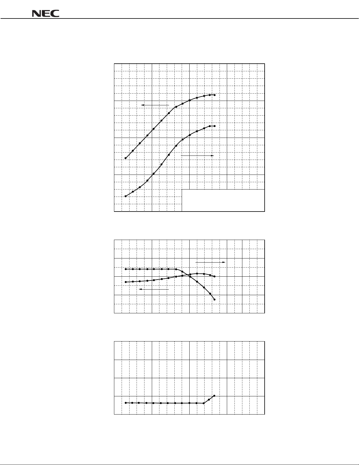
OUTPUT POWER AND POWER ADDED EFFICIENCY vs. INPUT POWER
NE960R2 SERIES
30
25
(dBm)
out
20
Output Power P
15
10
51015
200
f = 14.5 GHz (1 tone),
DS
= 9 V, I
Dset
V
g
= 1 kΩ
R
= 90 mA
20 25
Input Power Pin (dBm)
DRAIN CURRENT AND GAIN vs. INPUT POWER
60
45
(%)
add
η
30
Power Added Efficiency
15
0
14
150
(mA)
D
100
50
Drain Current I
0
5 10152025
1.5
1.0
(mA)
g
0.5
0.0
Gate Current I
–0.5
5 10152025
in
Input Power P
(dBm)
GATE CURRENT vs. INPUT POWER
in
Input Power P
(dBm)
12
10
Gain (dB)
8
6
Preliminary Data Sheet P13775EJ2V0DS00
3

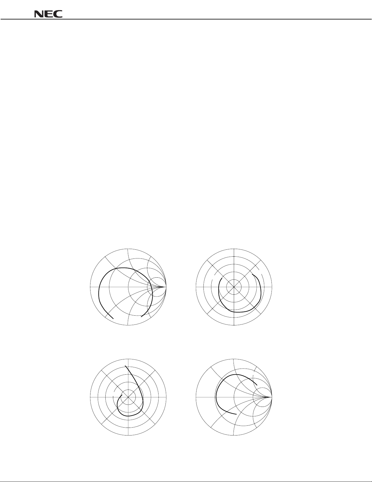
TYPICAL S-PARAMETER
[NE960R275]
NE960R2 SERIES
TEST CONDITIONS: VDS = 9 V, I
FREQUENCY S
11
Dset
= 90 mA
21
S
12
S
22
S
GHz MAG. ANG. (deg.) MAG. ANG. (deg.) MAG. ANG. (deg.) MAG. ANG. (deg.)
2.0
3.0
4.0
5.0
6.0
7.0
8.0
9.0
10.0
11.0
12.0
13.0
14.0
15.0
16.0
0.89
0.86
0.85
0.84
0.81
0.83
0.81
0.75
0.71
0.62
0.48
0.54
0.69
0.80
0.81
–113
–129
–138
–140
–144
–152
–163
–176
166
140
86
20
–20
–45
–66
3.99
2.88
2.29
1.99
1.78
1.77
1.82
1.89
2.12
2.42
2.50
2.32
1.77
1.30
1.03
98
80
65
51
39
27
15
–19
–44
–78
–113
–144
–166
167
0.057
0.058
0.057
0.057
0.059
0.060
0.062
0
0.062
0.064
0.072
0.074
0.065
0.049
0.040
0.039
34
15
10
–17
–46
–88
–132
–176
149
0.42
0.46
0.43
7
5
3
3
1
0
0.41
0.44
0.49
0.53
0.52
0.47
0.45
0.50
0.56
0.59
0.61
0.67
START 2 GHz, STOP 16 GHz, STEP 1 GHz
11
0.5
S
1.0
2.0
+135° +45°
S
+90°
12
–79
–85
–94
–110
–125
–135
–141
–150
–167
164
129
94
68
44
27
0.5 1.0 2.0
0
16 GHz
2 GHz
–0.5
–1.0
S
21
+90°
+135° +45°
±180° 0°
–135°
2 GHz
16 GHz
–90°
–2.0
R
max.
max.
R
= 1
–45°
= 5
16 GHz
∞
±180° 0
–135°
–90°
22
S
1.0
0.5
16 GHz
0.5 1.0 2.0
0
2 GHz
–0.5
–1.0
2 GHz
–45°
R
max.
2.0
–2.0
R
max.
= 0.1
∞
= 1
4
Preliminary Data Sheet P13775EJ2V0DS00
 Loading...