

Page 1
MM54HC181/MM74HC181
Arithmetic Logic Units/Function Generators
General Description
These arithmetic logic units (ALU)/function generators utilize advanced silicon-gate CMOS technology. They possess
the high noise immunity and low power consumption of
standard CMOS integrated circuits, as well as the ability to
drive 10 LS-TTL loads.
The MM54HC181/MM74HC181 are arithmetic logic unit
(ALU)/function generators that have a complexity of 75
equivalent gates on a monolithic chip. These circuits perform 16 binary arithmetic operations on two 4-bit words as
shown in Tables 1 and 2. These operations are selected by
the four function-select lines (S0, S1, S2, S3) and include
addition, subtraction, decrement, and straight transfer.
When performing arithmetic manipulations, the internal carries must be enabled by applying a low-level voltage to the
mode control input (M). A full carry look-ahead scheme is
made available in these devices for fast, simultaneous carry
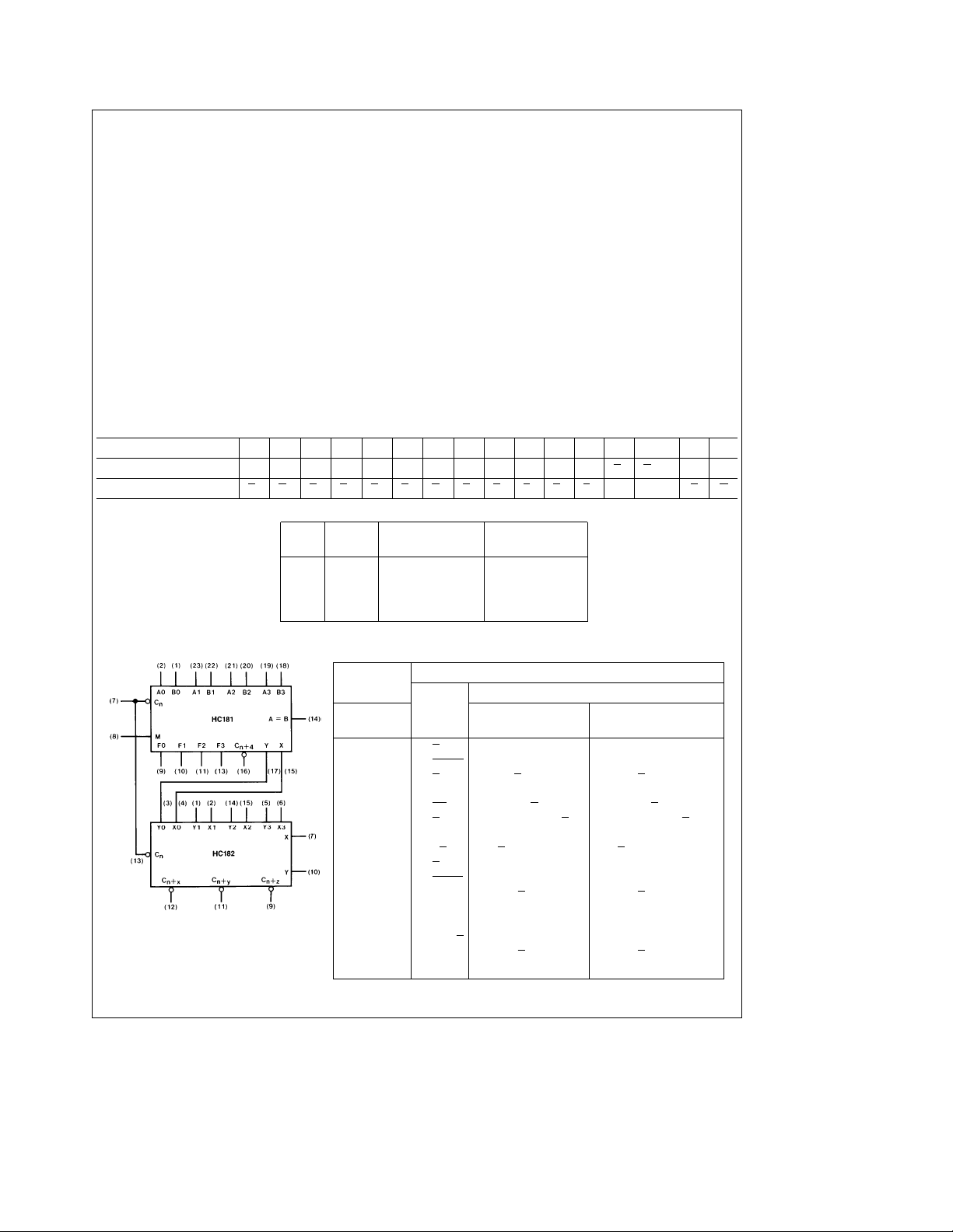
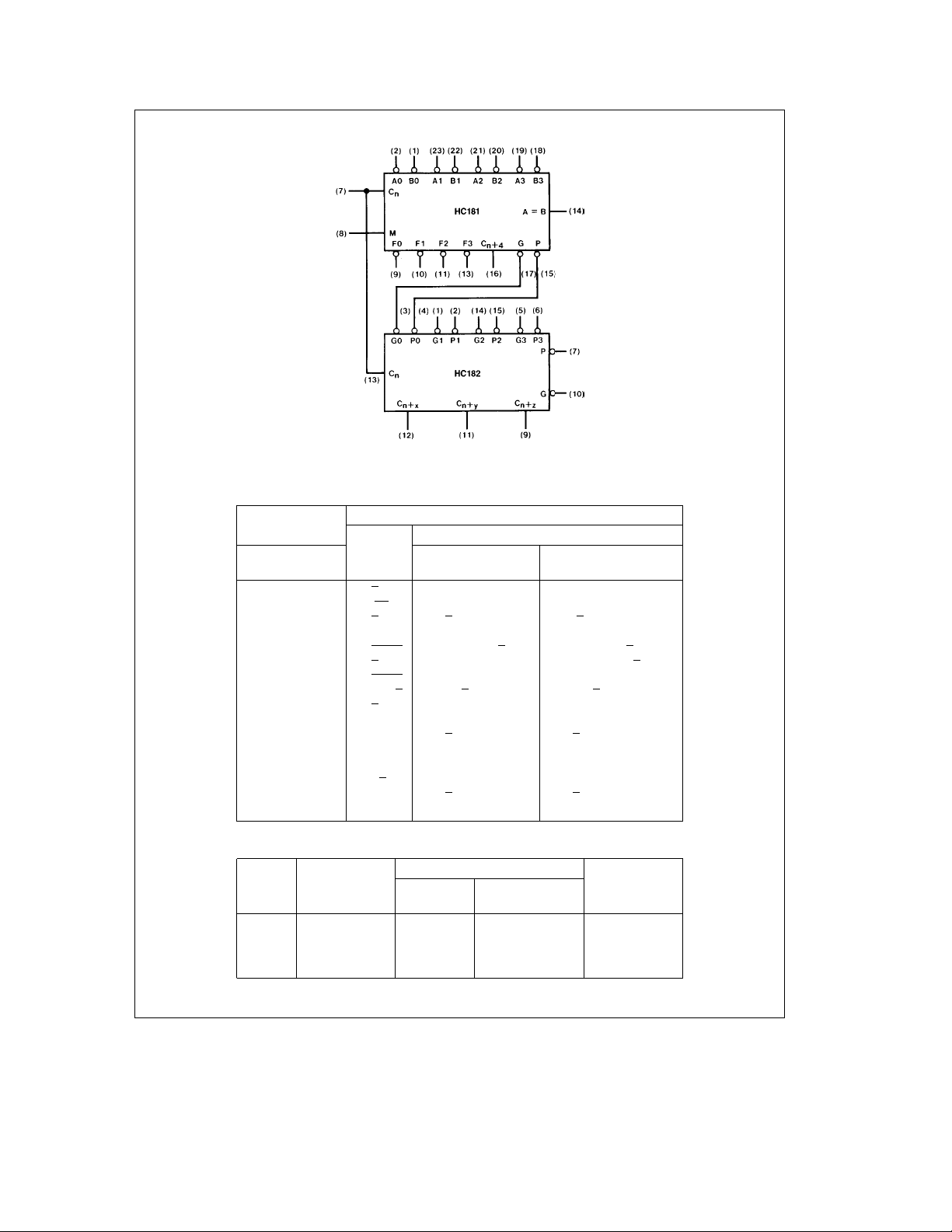
generation by means of two cascade-outputs (pins 15 and
17) for the four bits in the package. When used in conjunction with the MM54HC182 or MM74HC182, full carry lookahead circuits, high-speed arithmetic operations can be performed. The method of cascading HC182 circuits with these
ALU’s to provide multi-level full carry look-ahead is illustrated under typical applications data for the MM54HC182/
MM74HC182.
If high speed is not of importance, a ripple-carry input (C
and a ripple-carry output (C
the ripple-carry delay has also been minimized so that arithmetic manipulations for small word lengths can be performed without external circuitry.
Features
Y
Full look-ahead for high-speed operations on
long words
Y
Arithmetic operating modes:
Addition
Subtraction
Shift operand a one position magnitude comparison
Plus twelve other arithmetic operations
Y
Logic function modes:
Exclusive-OR
Comparator
AND, NAND, OR, NOR
Plus ten other logic operations
Y
Wide operating voltage range: 2V –6V
Y
Low input current: 1 mA maximum
Y
Low quiescent current: 80 mA maximum
January 1988
a
4) are available. However,
n
MM54HC181/MM74HC181 Arithmetic Logic Units/Function Generators
)
n
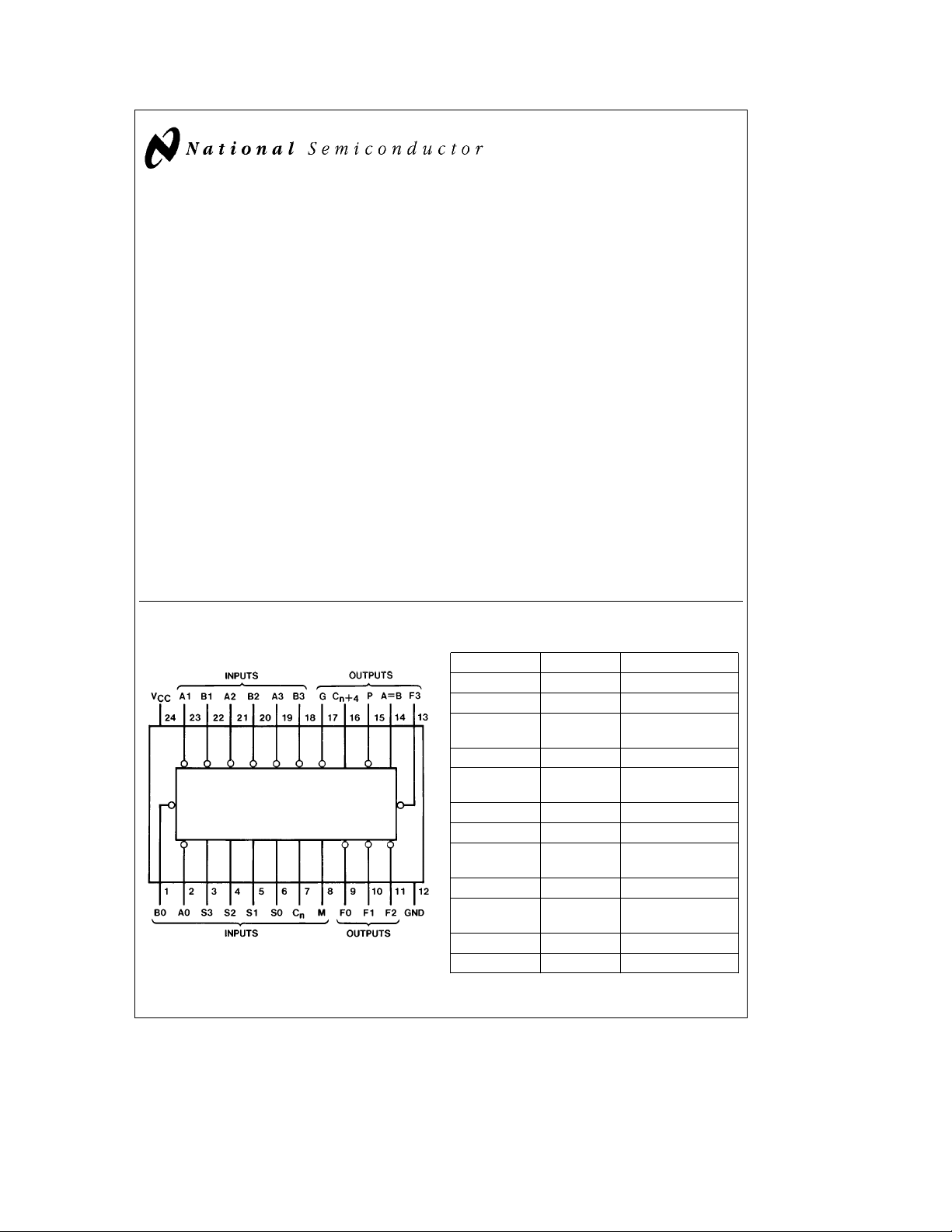
Connection Diagram
Dual-In-Line Package
Top View
Order Number MM54HC181 or MM74HC181
C
1995 National Semiconductor Corporation RRD-B30M105/Printed in U. S. A.
TL/F/5320
TL/F/5320– 1
Pin Designations
Designation Pin Nos. Function
A3, A2, A1, A0 19, 21, 23, 2 Word A Inputs
B3, B2, B1, B0 18, 20, 22, 1 Word B Inputs
S3, S2, S1, S0 3, 4, 5, 6
C
n
M8
F3, F2, F1, F0 13, 11, 10, 9 Function Outputs
AeB 14 Comparator Outputs
P15
a
C
4 16 Inv. Carry Output
n
G17
V
CC
GND 12 Ground
7 Inv. Carry Input
24 Supply Voltage
Function-Select
Inputs
Mode Control
Input
Carry Propagate
Output
Carry Generate
Output
Page 2
General Description (Continued)
These circuits will accommodate active-high or active-low
data, if the pin designations are interpreted as shown below.
Subtraction is accomplished by 1’s complement addition
where the 1’s complement of the subtrahend is generated
internally. The resultant output is AÐBÐ1, which requires
an end-around or forced carry to produce AÐB.
The 181 can also be utilized as a comparator. The A
e
output is internally decoded from the function outputs (F0,
F1, F2, F3) so that when two words of equal magnitude are
applied at the A and B inputs, it will assume a high level to
indicate equality (A
mode with C
e
A
B output is open-drain so that it can be wire-AND con-
e
B). The ALU should be in the subtract
e
H when performing this comparison. The
n
nected to give a comparison for more than four bits. The
carry output (C
magnitude information. Again, the ALU should be placed in
) can also be used to supply relative
na4
the subtract mode by placing the function select inputs S3,
S2, S1, S0 at L, H, H, L, respectively.
These circuits have been designed to not only incorporate
all of the designer’s requirements for arithmetic operations,
Pin Number 2 1 23 22 21 20 19 18 9 10 11 13 7 16 15 17
Active-High Data (Table 1) A0 B0 A1 B1 A2 B2 A3 B3 F0 F1 F2 F3 CnC
Active-Low Data (Table 1) A0B0A1B1A2B2A3B3F0F1F2F3CnC
but also to provide 16 possible functions of two Boolean
variables without the use of external circuitry. These logic
functions are selected by use of the four function-select inputs (S0, S1, S2, S3) with the mode-control input (M) at a
high level to disable the internal carry. The 16 logic functions are detailed in Tables 1 and 2 and include exclusiveOR, NAND, AND, NOR, and OR functions.
B
ALU SIGNAL DESIGNATIONS
The MM54HC181/MM74HC181 can be used with the signal
designations of either
Figure 1orFigure 2
The logic functions and arithmetic operations obtained with
signal designations as in
Figure 1
are given in Table 1; those
obtained with the signal designations of
in Table 2.
The 54HC/74HC logic family is speed, function, and pinout
compatible with the standard 54LS/74LS logic family. All
inputs are protected from damage due to static discharge by
internal diode clamps to V
and ground.
CC
.
Figure 2
na4
na4
are given
XY
P G
FIGURE 1
Input Output Active-High Data Active-Low Data
C
n
HH A
HL A
LH A
LL A
a
C
4 (Figure 1) (Figure 2)
n
s
BA
l
BA
k
BA
t
BA
Selection
MeHM
Logic
S3 S2 S1 S0 Functions C
e
H (no carry) C
n
LLLLFeA FeAF
LLLHF
LLHLFeABF
LLHHFe0F
LHLLF
eAa
BFeAaBF
e
a
A
e
e
AB FeA Plus AB FeA Plus AB Plus 1
Minus 1 (2’s Compl) FeZero
LHLHFeB Fe(AaB) Plus AB Fe(AaB) Plus AB Plus 1
LHHLF
LHHHF
e
AZBFeA Minus B Minus 1 FeA Minus B
e
AB FeAB Minus 1 FeAB
HLL LFeAaBFeA Plus AB FeA Plus AB Plus 1
HLLHFeAZBFeA Plus B FeA Plus B Plus 1
TL/F/5320– 2
HLHLF
e
BF
HLHHFeAB FeAB Minus 1 FeAB
HHL LFe1F
HHL HF
HHHLF
HHHHF
*Each bit is shifted to the next more significant position.
eAa
eAa
e
AF
e(Aa
e
A Plus A* FeA Plus A Plus 1
BFe(AaB) Plus A Fe(AaB) Plus A Plus 1
BFe(AaB) Plus A Fe(AaB) Plus A Plus 1
e
A Minus 1 FeA
t
B
k
B
l
B
s
B
Table I
Active High Data
e
L; Arithmetic Operations
e
L (with carry)
n
e
A Plus 1
e
(AaB) Plus 1
B F
e(Aa
B) Plus 1
B) Plus AB Fe(AaB) Plus AB Plus 1
2
Page 3
General Description (Continued)
Selection
S3 S2 S1 S0 Functions C
LLLLFeA FeA Minus 1 FeA
LLLHF
LLHLFeAaBFeAB Minus 1 Fe(AB)
LLHHFe1F
LHLLF
LHLHFeB FeAB Plus (AaB) FeAB Plus (AaB) Plus 1
LHHLF
LHHHF
HLLLF
HLLHFeAaBFeA Plus B FeA Plus B Plus 1
HLHLF
HLHHFeAaBFeAaBF
HHL LFe0F
HHLHF
HHHLF
HHHHF
*Each bit is shifted to the next more significant position.
eAa
eAa
eAa
e
e
e
e
e
TL/F/5320– 3
FIGURE 2
Table II
Active Low Data
MeHM
e
L; Arithmetic Operations
Logic
e
L (no carry) C
n
e
AB FeAB Minus 1 FeAB
e
Minus 1 (2’s Compl) FeZero
BFeA Plus (AaB)F
e
H (with carry)
n
e
A Plus (AaB) Plus 1
BFeA Minus B Minus 1 FeA Minus B
BFeAaB Fe(AaB Plus 1
ABF
BF
e
A Plus (AaB) FeA Plus (AaB) Plus 1
e
AB Plus (AaB) FeAB Plus (AaB) Plus 1
e
A Plus A* FeA Plus A Plus 1
e
(AaB) Plus 1
AB FeAB Plus A FeAB Plus A Plus 1
AB FeAB Plus A FeAB Plus A Plus 1
AF
e
AF
e
A Plus 1
Number Package Count Carry Method
of
Bits
Typical
Addition Times
Arithmetic/ Look Ahead
Logic Units Carry Generators
Between
ALU’s
1 to 4 20 ns 1 0 None
5 to 8 30 ns 2 0 Ripple
9 to 16 30 ns 3 or 4 1 Full Look-Ahead
17 to 64 50 ns 5 to 16 2 to 5 Full Look-Ahead
3
Page 4

Absolute Maximum Ratings (Notes1&2)
Operating Conditions
If Military/Aerospace specified devices are required,
please contact the National Semiconductor Sales
Office/Distributors for availability and specifications.
Supply Voltage (V
CC
)
DC Input Voltage (VIN)
DC Output Voltage (V
OUT
)
Clamp Diode Current (IIK,IOK)
DC Output Current, per pin (I
OUT
)
DC VCCor GND Current, per pin (ICC)
Storage Temperature Range (T
STG
b
b
)
b
0.5 toa7.0V
1.5 to V
CC
0.5 to V
CC
g
g
b
g
65§Ctoa150§C
a
1.5V
a
0.5V
20 mA
25 mA
50 mA
Supply Voltage (V
)26V
CC
DC Input or Output Voltage 0 V
(V
IN,VOUT
)
Operating Temp. Range (TA)
MM74HC
MM54HC
Input Rise or Fall Times
e
V
2.0V(tr,tf) 1000 ns
CC
e
V
4.5V 500 ns
CC
e
V
6.0V 400 ns
CC
Power Dissipation (PD)
(Note 3) 600 mW
S.O. Package only 500 mW
Lead Temperature (T
)
L
(Soldering 10 seconds) 260§C
DC Electrical Characteristics (Note 4)
e
T
25§C
Symbol Parameter Conditions V
CC
A
Typ Guaranteed Limits
V
Minimum High Level 2.0V 1.5 1.5 1.5 V
IH
Input Voltage 4.5V 3.15 3.15 3.15 V
6.0V 4.2 4.2 4.2 V
V
Maximum Low Level 2.0V 0.5 0.5 0.5 V
IL
Input Voltage** 4.5V 1.35 1.35 1.35 V
6.0V 1.8 1.8 1.8 V
V
I
LKG
V
Minimum High Level V
OH
Output Voltage
(any output except 4.5V 4.5 4.4 4.4 4.4 V
e
A
B) 6.0V 6.0 5.9 5.9 5.9 V
Maximum Leakage V
Open Drain Output Current V
(AeB Output)
Maximum Low Level V
OL
Output Voltage
e
VIHor V
l
V
l
l
l
IN
I
OUT
IN
I
OUT
I
OUT
IN
OUT
IN
I
OUT
e
e
e
IL
s
20 mA 2.0V 2.0 1.9 1.9 1.9 V
l
VIHor V
IL
s
4.0 mA 4.5V 4.2 3.98 3.84 3.7 V
l
s
5.2 mA 6.0V 5.7 5.48 5.34 5.2 V
l
VIHor V
e
V
CC
VIHor V
s
20 mA 2.0V 0 0.1 0.1 0.1 V
l
6.0V 0.5 5.0 10 mA
IL
IL
4.5V 0 0.1 0.1 0.1 V
6.0V 0 0.1 0.1 0.1 V
e
V
VIHor V
IN
I
l
OUT
I
l
OUT
I
IN
I
CC
Maximum Input V
Current
Maximum Quiescent V
Supply Current I
Note 1: Absolute Maximum Ratings are those values beyond which damage to the device may occur.
Note 2: Unless otherwise specified all voltages are referenced to ground.
Note 3: Power Dissipation temperature derating Ð plastic ‘‘N’’ package:
Note 4: For a power supply of 5V
with this supply. Worst case V
) occur for CMOS at the higher voltage and so the 6.0V values should be used.
I
OZ
** V
limits are currently tested at 20% of VCC. The above VILspecification (30% of VCC) will be implemented no later than Q1, CY’89.
IL
g
10% the worst case output voltages (VOH, and VOL) occur for HC at 4.5V. Thus the 4.5V values should be used when designing
and VILoccur at V
IH
IN
IN
OUT
CC
e
e
e
IL
s
4.0 mA 4.5V 0.2 0.26 0.33 0.4 V
l
s
5.2 mA 6.0V 0.2 0.26 0.33 0.4 V
l
VCCor GND 6.0V
g
0.1
VCCor GND 6.0V 8.0 80 160 mA
e
0 mA
b
12 mW/§C from 65§Cto85§C; ceramic ‘‘J’’ package:b12 mW/§C from 100§Cto125§C.
5.5V and 4.5V respectively. (The VIHvalue at 5.5V is 3.85V.) The worst case leakage current (IIN,ICC, and
74HC 54HC
eb
T
40 to 85§CT
A
g
1.0
Min Max Units
V
§
§
Units
b
b
40
55
A
eb
CC
a
85
a
125
55 to 125§C
g
1.0 mA
C
C
4
Page 5

AC Electrical Characteristics V
CC
e
5V, T
A
Symbol Parameter Conditions Typ
t
PHL,tPLH
t
PHL,tPLH
t
PHL,tPLH
t
PHL,tPLH
t
PHL,tPLH
t
PHL,tPLH
t
PHL,tPLH
t
PHL,tPLH
t
PHL,tPLH
t
PHL,tPLH
t
PHL,tPLH
t
PHL,tPLH
Maximum Propagation 13 20 ns
Delay from C
a
to C
4
n
n
Maximum Propagation Me0V, S0eS3eVCC30 45 ns
Delay from any S1
AorBtoC
a
4 (Sum mode)
N
eS0e
0V
Maximum Propagation Me0V, S0eS3e0V 30 45 ns
Delay from any S1
AorBtoC
a
4 (Diff. mode)
N
eS2e
V
CC
Maximum Propagation Me0V 20 30 ns
Delay from C
Maximum Propagation Me0V, S0
Delay from any S3
AorBtoG S1eS2e0V
Maximum Propagation Me0V, S0
Delay from any S3
AorBtoG S1
Maximum Propagation Me0V, S0
Delay from any S3
AorBtoP S1eS2e0V
Maximum Propagation Me0V, S0
Delay from any S3
AorBtoP S1eS2eV
Maximum Propagation Me0V, S0
Delay from A
Maximum Propagation Me0V, S0
Delay from A
Maximum Propagation MeV
Delay from A
Maximum Propagation Me0V, S0
to any F (Sum or
n
Diff.
e
(Sum
e
eS2e
mode)
V
CC
mode)
0V
(Diff mode)
e
V
CC
(Sum
mode)
e
0V
(Diff mode)
or BIto FIS3eV
I
or BIto FIS3e0V
I
CC
S1eS2e0V
(Sum
mode)
eS2e
S1
(Diff mode)
or BIto FI(Logic mode)
I
CC
e
e
V
CC
e
e
CC
e
e
V
CC
e
Delay from any S3e0V
AorBtoA
e
BS1
e
S2eV
(Diff mode)
CC
e
25§C, C
L
e
15 pF, t
Guaranteed
Limit
20 30 ns
20 30 ns
27 41 ns
24 37 ns
20 30 ns
19 29 ns
25 37 ns
25 37 ns
e
r
Units
e
t
6ns
f
5
Page 6

AC Electrical Characteristics C
e
L
Symbol Parameter Conditions V
t
PHL,tPLH
t
PHL,tPLH
t
PHL,tPLH
t
PHL,tPLH
t
PHL,tPLH
t
PHL,tPLH
t
PHL,tPLH
t
PHL,tPLH
t
PHL,tPLH
t
PHL,tPLH
t
PHL,tPLH
t
PHL,tPLH
t
TLH,tTHL
C
PD
C
IN
Note 5: CPDdetermines the no load dynamic power consumption, P
Maximum Propagation 2.0V 125 155 190 ns
Delay from C
Maximum Propagation Me0V, S0
Delay from any S3eV
AorBtoC
Maximum Propagation Me0V, S0
Delay from any S3e0V 4.5V 50 63 75 ns
AorBtoC
Maximum Propagation Me0V 2.0V 65 150 190 225 ns
Delay from Cnto any F (Sum or 4.5V 22 32 40 48 ns
Maximum Propagation Me0V, S0
Delay from any S3
AorBtoG S1eS2e0V 6.0V 12 30 38 45 ns
Maximum Propagation Me0V, S0
Delay from any S3
AorBtoG S1eS2 6.0V 16 29 37 44 ns
Maximum Propagation Me0V, S0
Delay from any S3
AorBtoP S1eS2e0V 6.0V 25 37 47 56 ns
Maximum Propagation Me0V, S0
Delay from any S3
AorBtoP S1eS2eVCC6.0V 24 34 43 51 ns
Maximum Propagation Me0V, S0
Delay from A
Maximum Propagation Me0V, S0
Delay from A
Maximum Propagation MeV
Delay from A
Maximum Propagation Me0V, S0
Delay from any S3
AorBtoA
Maximum Output Rise 2.0V 30 75 95 110 ns
and Fall Time 4.5V 8 15 19 22 ns
Power Dissipation 300 pF
Capacitance (Note 5)
Maximum Input 5 15 15 15 pF
Capacitance
a
to C
4 4.5V 25 31 38 ns
n
n
e
a
4S1
n
a
4S1
n
or BIto FIS3eV
I
or BIto FIS3e0V 4.5V 32 40 48 ns
I
or BIto FI(Logic mode) 4.5V 30 40 50 60 ns
I
e
BS1
CC
e
S2e0V 6.0V 30 43 53 65 ns
mode)
(Sum
e
e
S2eVCC6.0V 43 53 65 ns
mode)
(Diff
mode) 6.0V 14 28 35 42 ns
Diff
e
e
VCC, 4.5V 20 35 44 53 ns
mode)
(Sum
e
e
0V 4.5V 23 33 42 50 ns
mode)
(Diff
e
e
V
CC
mode)
(Sum
e
e
0V 4.5V 27 39 49 60 ns
mode)
(Diff
e
CC
S1eS2e0V 6.0V 21 31 39 47 ns
mode)
(Sum
e
S1eS2eVCC6.0V 27 34 41 ns
mode)
(Diff
CC
e
e
0V 4.5V 30 40 50 60 ns
e
S2eVCC6.0V 23 34 43 51 ns
(Diff mode)
D
e
50 pF, t
CC
e
t
6 ns (unless otherwise specified)
r
f
e
T
25§C
A
eb
T
A
74HC 54HC
40 to 85§CT
eb
A
55 to 125§C
Typ Guaranteed Limits
6.0V 22 28 33 ns
2.0V 110 250 325 375 ns
4.5V 35 50 63 75 ns
2.0V 250 325 375 ns
2.0V 70 175 220 263 ns
2.0V 65 165 210 250 ns
2.0V 80 220 275 330 ns
4.5V 30 44 55 66 ns
2.0V 75 195 244 293 ns
2.0V 70 180 225 270 ns
4.5V 26 36 45 54 ns
2.0V 160 200 290 ns
2.0V 180 200 250 300 ns
6.0V 23 34 43 51 ns
2.0V 180 200 250 300 ns
6.0V 7 13 16 19 ns
2
e
CPDV
faICCVCC, and the no load dynamic current consumption, I
CC
e
CPDVCCfaICC.
S
Units
6
Page 7

Parameter Measurement Information
Logic Mode Test Table Function Inputs: S1eS2eMeVCC,S0eS3e0V
Parameter Under
t
PHL,tPLH
t
PHL,tPLH
Input Same Bit Output
Test
A
I
B
I
Other Input
Apply Apply Apply Apply
V
CC
B
I
A
I
GND V
None None
None None
SUM Mode Test Table Function Inputs: S0eS3eV
Parameter Under
t
PHL,tPLH
t
PHL,tPLH
t
PHL,tPLH
t
PHL,tPLH
t
PHL,tPLH
t
PHL,tPLH
t
PHL,tPLH
t
PHL,tPLH
t
PHL,tPLH
Input Same Bit Output
Test
A
I
B
I
A
I
B
I
A
I
B
I
C
n
A
I
B
I
Other Input
Apply Apply Apply Apply
V
CC
B
I
A
I
B
I
A
I
None B
None A
GND V
None
None
None None
None None
I
I
None None
None B
None A
I
I
Diff Mode Test Table Function Inputs: S1eS2eVCC,S0eS3eMe0V
Parameter Under
t
PHL,tPLH
t
PHL,tPLH
t
PHL,tPLH
t
PHL,tPLH
t
PHL,tPLH
t
PHL,tPLH
t
PHL,tPLH
t
PHL,tPLH
t
PHL,tPLH
t
PHL,tPLH
t
PHL,tPLH
Input Same Bit Output
Test
A
I
B
I
A
I
B
I
A
I
B
I
A
I
B
I
C
n
A
I
B
I
Other Input
Apply Apply Apply Apply
V
CC
None B
A
I
None B
A
I
B
I
None A
None B
A
I
GND V
I
None
I
None None
None None
I
I
None
None None
B
I
None A
None None
I
Other Data Inputs
CC
S1eS2eMe0V
CC
Remaining
A and B, C
Remaining
A and B, C
Other Data Inputs
CC
Remaining
A and B
Remaining
A and B
Remaining
A and B, C
Remaining
A and B, C
Remaining Remaining
BA,C
Remaining Remaining
BA,C
All All Any F
A B or C
Remaining Remaining
BA,C
Remaining Remaining
BA,C
Other Data Inputs
CC
Remaining Remaining
AB,C
Remaining Remaining
AB,C
None
None
Remaining Remaining
AB,C
Remaining Remaining
AB,C
All
A and B or any F
Remaining
A and B, C
Remaining
A and B, C
Remaining
A and B, C
Remaining
A and B, C
Remaining
None
Remaining
7
GND
GND
C
n
C
n
n
n
n
n
GND
n
n
n
n
None
A, B, C
A, B, C
Under
Test
F
n
n
n
n
I
F
I
Under
Test
F
I
F
I
P In-Phase
P In-Phase
Output
Waveform
Out-of-Phase
Out-of-Phase
Output
Waveform
In-Phase
In-Phase
G In-Phase
G In-Phase
a
4
n
a
C
4 Out-of-Phase
n
a
C
4 Out-of-Phase
n
Under
Test
F
I
F
I
n
n
n
n
P In-Phase
P Out-of-Phase
G In-Phase
G Out-of-Phase
e
A
B In-Phase
In-Phase
Output
Waveform
In-Phase
Out-of-Phase
AeB Out-of-Phase
a
4
C
n
a
C
4 Out-of-Phase
n
n
n
a
C
4 In-Phase
n
In-Phase
Page 8

Logic Diagram
e
V
PIN 24
CC
e
GND
PIN 12
TL/F/5320– 4
8
Page 9

Physical Dimensions inches (millimeters)
Ceramic Dual-In-Line Package (J)
Order Number MM54HC181J or MM74HC181J
NS Package Number J24F
9
Page 10

Physical Dimensions inches (millimeters) (Continued)
Molded Dual-In-Line Package (N)
Order Number MM74HC181N
NS Package Number N24C
LIFE SUPPORT POLICY
MM54HC181/MM74HC181 Arithmetic Logic Units/Function Generators
NATIONAL’S PRODUCTS ARE NOT AUTHORIZED FOR USE AS CRITICAL COMPONENTS IN LIFE SUPPORT
DEVICES OR SYSTEMS WITHOUT THE EXPRESS WRITTEN APPROVAL OF THE PRESIDENT OF NATIONAL
SEMICONDUCTOR CORPORATION. As used herein:
1. Life support devices or systems are devices or 2. A critical component is any component of a life
systems which, (a) are intended for surgical implant support device or system whose failure to perform can
into the body, or (b) support or sustain life, and whose be reasonably expected to cause the failure of the life
failure to perform, when properly used in accordance support device or system, or to affect its safety or
with instructions for use provided in the labeling, can effectiveness.
be reasonably expected to result in a significant injury
to the user.
National Semiconductor National Semiconductor National Semiconductor National Semiconductor
Corporation Europe Hong Kong Ltd. Japan Ltd.
1111 West Bardin Road Fax: (
Arlington, TX 76017 Email: cnjwge@tevm2.nsc.com Ocean Centre, 5 Canton Rd. Fax: 81-043-299-2408
Tel: 1(800) 272-9959 Deutsch Tel: (
Fax: 1(800) 737-7018 English Tel: (
National does not assume any responsibility for use of any circuitry described, no circuit patent licenses are implied and National reserves the right at any time without notice to change said circuitry and specifications.
Fran3ais Tel: (
Italiano Tel: (
a
49) 0-180-530 85 86 13th Floor, Straight Block, Tel: 81-043-299-2309
a
49) 0-180-530 85 85 Tsimshatsui, Kowloon
a
49) 0-180-532 78 32 Hong Kong
a
49) 0-180-532 93 58 Tel: (852) 2737-1600
a
49) 0-180-534 16 80 Fax: (852) 2736-9960
 Loading...