

Page 1

查询DM8556供应商
DM7556/DM8556 TRI-STATEÉProgrammable
Binary Counters
DM7556/DM8556 TRI-STATE Programmable Binary Counters
August 1989
General Description
These circuits are synchronous, edge-sensitive, fully-programmable 4-bit counters. The counters feature both conventional totem-pole and TRI-STATE outputs; such that
when the outputs are in the high impedance mode, they can
be used to enter data from the bus lines. In addition, the
clear input operates completely independent of all other inputs. During the programming operation, data is loaded into
the flip-flops on the positive-going edge of the clock pulse.
To facilitate cascading of these counters, the MAX COUNT
output can be tied directly into the count enable input of the
next counter.
Connection Diagram
Dual-In-Line Package
Order Number DM7556J or DM8556N
See NS Package Number J16A or N16A
Features
Y
Typical clock frequency 35 MHz
Y
TRI-STATE outputs
Y
Fully independent clear
Y
Synchronous loading
Y
Cascading circuitry provided internally
TL/F/6588– 1
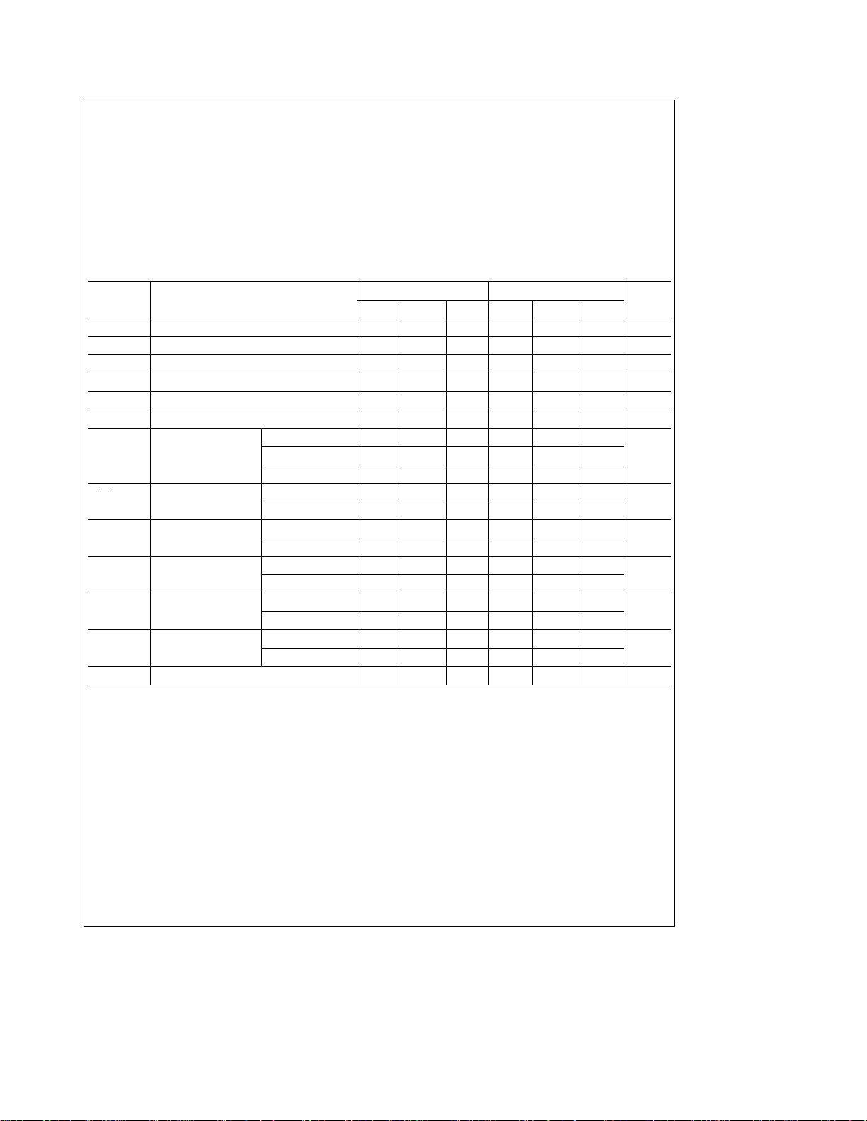
Function Table
Control Inputs I/O Ports Active Outputs
LOAD CE CLK OD Reset I/OAI/OBI/OCI/ODQAQBQCQ
HXXLH L L L LLLLL
HXXHH Z Z Z ZLLLL
HXLL LQ
HXLHL ZZZ ZQA0QB0QC0Q
LH
HL
HL
The I/O pins are used as inputs when they are TRI-STATED, and the LOAD input is Low. They are outputs and active
when LOAD
H
L
X
a, b, c, d
Q
TRI-STATEÉis a registered trademark of the National Semiconductor Corporation.
C
1995 National Semiconductor Corporation RRD-B30M105/Printed in U. S. A.
were established.
input is High and OD is Low.
e
High Level (Steady State)
e
Low Level (Steady State)
e
Don’t Care including transitions
e
The level of the steady state input at inputs A, B, C, D respectively
A0,QB0,QC0,QD0
LL ab cdABCD
u
L L COUNT COUNT
u
H L Z Z Z Z COUNT
u
e
The level of QA,QB,QC,QDrespectively, before the indicated steady state input conditions
TL/F/6588
A0QB0QC0QD0QA0QB0QC0QD0
D
D0
Page 2
Absolute Maximum Ratings (Note)
If Military/Aerospace specified devices are required,
please contact the National Semiconductor Sales
Office/Distributors for availability and specifications.
Supply Voltage 7V
Input Voltage 5.5V
Operating Free Air Temperature Range
DM75
DM85 0
Storage Temperature Range
b
55§Ctoa125§C
Ctoa70§C
§
b
65§Ctoa150§C
Recommended Operating Conditions
Symbol Parameter
V
CC
V
IH
V
IL
I
OH
I
OL
f
CLK
t
W
t
CE
t
SETUP(1)
t
HOLD(1)
t
SETUP(0)
t
HOLD(0)
T
A
Note 1: T
Supply Voltage 4.5 5 5.5 4.75 5 5.25 V
High Level Input Voltage 2 2 V
Low Level Input Voltage 0.8 0.8 V
High Level Output Current
Low Level Output Current 16 16 mA
Clock Frequency (Note 1) 0 25 0 25 MHz
Pulse Width Clock 25 25
(Note 1)
Clear 20 20 ns
Load 30 30
Count Enable Setup 30 30
Time (Note 1)
Hold
Setup Time High Data 25 25
Logic Level (Note 1)
Load 30 30
Hold Time High Data 5 5
Logic Level (Note 1)
Load
Setup Time Low Data 30 30
Logic Level (Note 1)
Load 25 25
Hold Time Low Data 5 5
Logic Level (Note 1)
Load
Free Air Operating Temperature
e
A
25§C and V
e
5V.
CC
Note:
The ‘‘Absolute Maximum Ratings’’ are those values
beyond which the safety of the device cannot be guaranteed. The device should not be operated at these limits. The
parametric values defined in the ‘‘Electrical Characteristics’’
table are not guaranteed at the absolute maximum ratings.
The ‘‘Recommended Operating Conditions’’ table will define
the conditions for actual device operation.
DM7556 DM8556
Min Nom Max Min Nom Max
b
2
b
10
b
10
b
10
b
55 125 0 70
b
10
b
10
b
10
b
Units
5.2 mA
ns
ns
ns
ns
ns
§
C
2
Page 3
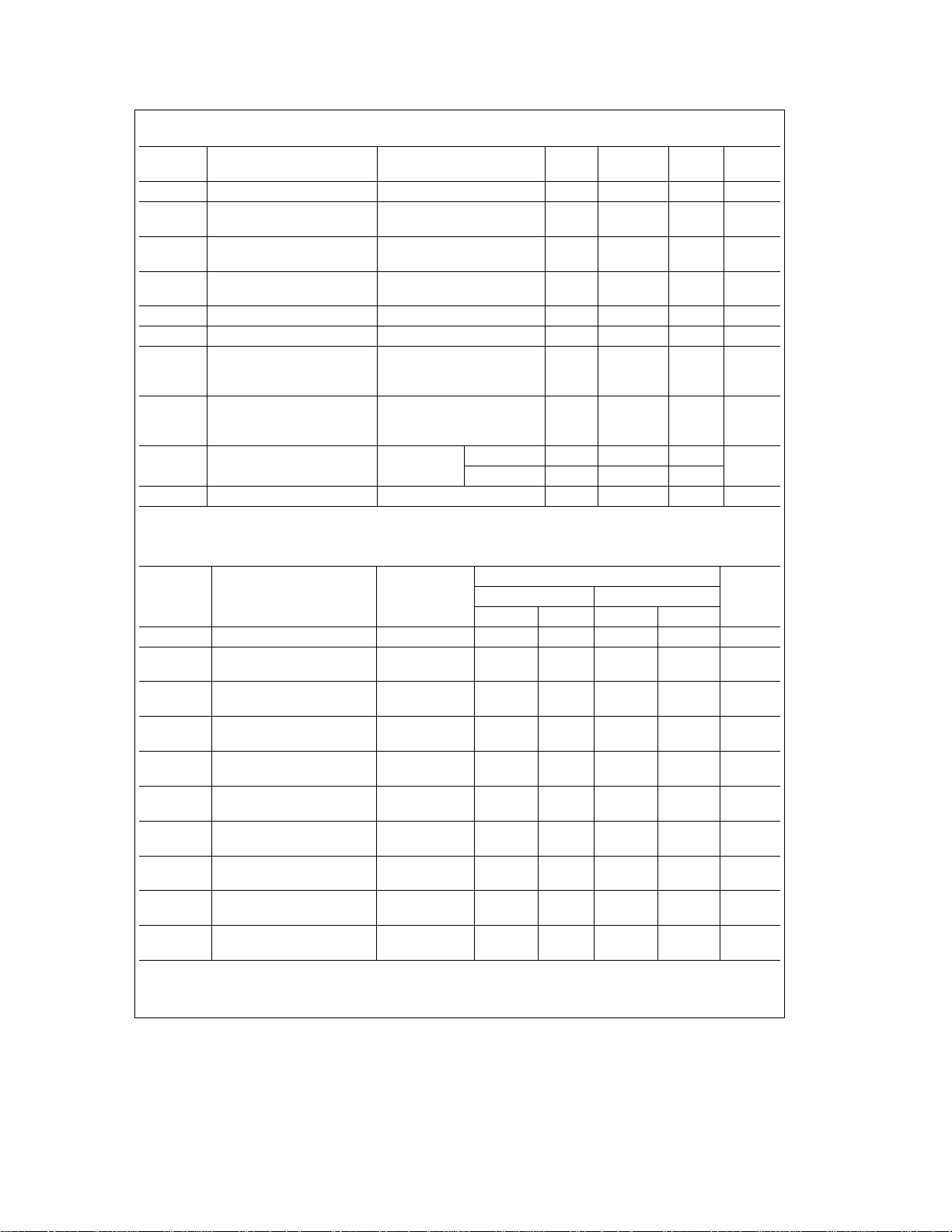
Electrical Characteristics over recommended operating free air temperature range (unless otherwise noted)
Symbol Parameter Conditions Min
e
V
V
V
I
I
I
IH
I
IL
I
OZH
I
OH
OL
Input Clamp Voltage V
High Level Output V
Voltage V
Low Level Output V
Voltage V
Input Current@Max V
Input Voltage
High Level Input Current V
Low Level Input Current V
Off-State Output Current with V
High Level Output V
Voltage Applied
I
OZL
Off-State Output Current with V
Low Level Output V
Voltage Applied
I
OS
I
CC
Note 1: All typicals are at V
Note 2: Not more than one output should be shorted at a time.
Short Circuit V
Output Current (Note 2)
Supply Current V
e
e
5V, T
CC
25§C.
A
CC
CC
IL
CC
IH
CC
CC
CC
CC
IH
CC
IH
CC
CC
e
e
e
e
eb
Min, I
e
Min, I
Max, V
e
Min, I
Min, V
e
Max, V
e
Max, V
e
Max, V
e
Max, V
Min, V
e
Max, V
Min, V
e
Max DM75
e
Max 75 100 mA
12 mA
I
e
Max
OH
e
Min
IH
e
Max
OL
e
Max
IL
e
5.5V
I
e
2.4V 40 mA
I
e
0.4V
I
e
2.4V
O
e
Max 40 mA
IL
e
0.4V
O
e
Max
IL
DM85
2.4 V
b
b
25
25
Typ
(Note 1)
Max Units
b
1.5 V
0.4 V
1mA
b
1.6 mA
b
40 mA
b
70
b
70
mA
Switching Characteristics at V
Symbol Parameter
f
MAX
t
PLH
t
PHL
t
PLH
t
PHL
t
PHL
t
PZH
t
PZL
t
PHZ
t
PLZ
Maximum Clock Frequency 25 MHz
Propagation Delay Time Clock to
Low to High Level Output Output
Propagation Delay Time Clock to
High to Low Level Output Output
Propagation Delay Time Clock to
Low to High Level Output MAX-CNT
Propagation Delay Time Clock to
High to Low Level Output MAX-CNT
Propagation Delay Time Reset to
High to Low Level Output Output
Output Enable Time Output
to High Level Output Disable to Q
Output Enable Time Output
to Low Level Output Disable to Q
Output Disable Time Output
from High Level Output Disable to Q
Output Disable Time Output
from Low Level Output Disable to Q
e
5V and T
CC
From (Input)
To (Output)
e
25§C (See Section 1 for Test Waveforms and Output Load)
A
e
400X
R
L
e
C
5pF C
L
e
50 pF Units
L
Min Max Min Max
22 ns
44 ns
33 ns
33 ns
44 ns
20 ns
20 ns
12 ns
20 ns
3
Page 4

Logic Diagram
TL/F/6588– 2
75/8556
4
Page 5

Timing Diagram
75/8556 Typical Clear, Preset, Count, Inhibit Sequence
Sequence
(1) Clear to zero.
(2) Load binary five.
(3) Count six, seven, eight, nine, ten, eleven, twelve, thirteen, fourteen, fifteen, zero.
(4) Disable TRI-STATE outputs.
(5) Disable counter.
(6) Count to one.
5
TL/F/6588– 3
Page 6

Switching Time Waveforms
Clock and Reset Voltage
Count Enable and Clock
Load, Data and Clock
Output Disable
TL/F/6588– 4
TL/F/6588– 5
TL/F/6588– 6
TL/F/6588– 7
6
Page 7

Physical Dimensions inches (millimeters)
Ceramic Dual-In-Line Package (J)
Order Number DM7556J
NS Package Number J16A
7
Page 8

Physical Dimensions inches (millimeters) (Continued)
Molded Dual-In-Line Package (N)
Order Number DM8556N
NS Package Number N16A
DM7556/DM8556 TRI-STATE Programmable Binary Counters
LIFE SUPPORT POLICY
NATIONAL’S PRODUCTS ARE NOT AUTHORIZED FOR USE AS CRITICAL COMPONENTS IN LIFE SUPPORT
DEVICES OR SYSTEMS WITHOUT THE EXPRESS WRITTEN APPROVAL OF THE PRESIDENT OF NATIONAL
SEMICONDUCTOR CORPORATION. As used herein:
1. Life support devices or systems are devices or 2. A critical component is any component of a life
systems which, (a) are intended for surgical implant support device or system whose failure to perform can
into the body, or (b) support or sustain life, and whose be reasonably expected to cause the failure of the life
failure to perform, when properly used in accordance support device or system, or to affect its safety or
with instructions for use provided in the labeling, can effectiveness.
be reasonably expected to result in a significant injury
to the user.
National Semiconductor National Semiconductor National Semiconductor National Semiconductor
Corporation Europe Hong Kong Ltd. Japan Ltd.
1111 West Bardin Road Fax: (
Arlington, TX 76017 Email: cnjwge@tevm2.nsc.com Ocean Centre, 5 Canton Rd. Fax: 81-043-299-2408
Tel: 1(800) 272-9959 Deutsch Tel: (
Fax: 1(800) 737-7018 English Tel: (
National does not assume any responsibility for use of any circuitry described, no circuit patent licenses are implied and National reserves the right at any time without notice to change said circuitry and specifications.
Fran3ais Tel: (
Italiano Tel: (
a
49) 0-180-530 85 86 13th Floor, Straight Block, Tel: 81-043-299-2309
a
49) 0-180-530 85 85 Tsimshatsui, Kowloon
a
49) 0-180-532 78 32 Hong Kong
a
49) 0-180-532 93 58 Tel: (852) 2737-1600
a
49) 0-180-534 16 80 Fax: (852) 2736-9960
 Loading...