

Page 1
DM9131
10/100 Mbps Fast Ethernet Physical Layer Si ngle Chi p Transceiver
Final 1
Version: DM9131-DS-F01
April 7, 2000
General Description
The DM9131 is a physical-layer, single-chip, lowpower transceiver for 100BASE-TX and 10BASE-T
operations. On the media side, it provides a direc t
interface either to Unshielded Twisted Pair Cable 5
(UTP5) for 100BASE-TX Fast Ethernet, or
UTP5/UTP3 Cable for 10BASE-T Ethernet, and it also
provides PECL interface to connect the external fiber
optical transceiver. Through the Media Independent
Interface (MII), the DM9131 connects to the Medium
Access Control (MAC) layer, ensuring a high interoperability among products from different vendors.
The DM9131 uses a low-power and high-performance
CMOS process. It contains the entire physical layer
functi ons of 100BASE-TX as defined by IEEE802.3u,
including the Physical Coding Sublayer (PCS),
Physical M edium A ttachm ent (PMA), Twisted Pair
Physical Medium Dependent Sublayer (T P-PMD),
10BASE-TX Encoder/Decoder (ENC/DEC), and
Twisted Pair Media Access Unit (TPMAU). The
DM9131 provides a strong support for the autonegotiation function utilizing automatic media speed
and protocol selection. Furthermore, due to the builtin wave-shaping filter, the DM9131 needs no external
filter to transport signals to the media in 100M or 10M
Ethernet operat ion.
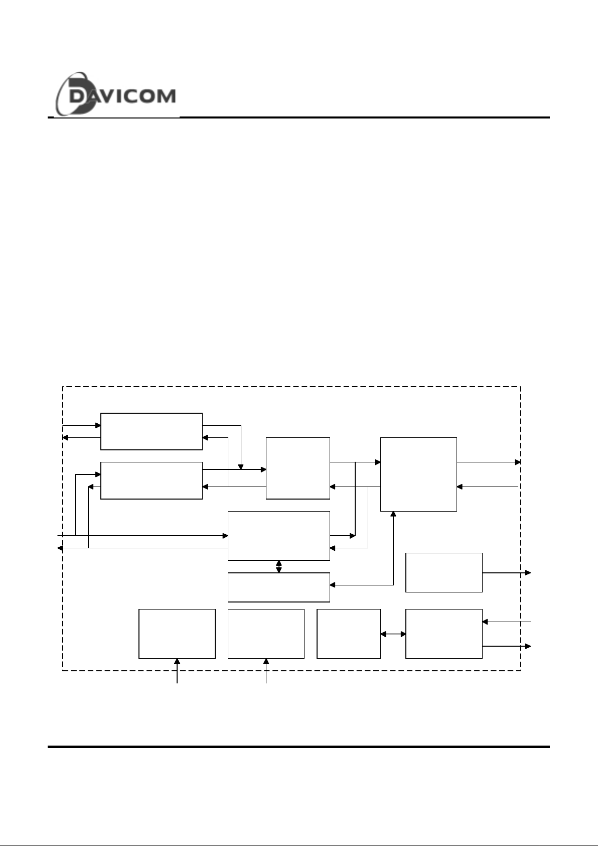
Block Diagram
MII
Management
Control
Biasing/
Power
Block
Clock
Circuit
Block
100Base-TX
Transceiver
100Base-FX
PECL
Interface
LED Driver
MII
Interface
MII
Register
100Base-
TX
PCS
10Base-T
TX/RX Module
Auto-Negotiation
Page 2

DM9131
10/100 Mbps Fast Ethernet Physical Layer Si ngle Chi p Transceiver
2 Final
Version: DM9131-DS-F01
April 7, 2000
Table of Contents
General Descri pt ion................................................1
Block Diagram........................................................1
Features.................................................................3
Pin Configuration: DM9101E LQFP ........................4
Pin Description.......................................................5
T
Normal MII Interface, 21 pins...............................5
T
Media Interface, 5 pi ns........................................6
T
LED Inte r face, 5 pins...........................................6
T
Mode, 11 pins......................................................7
T
Bias and Clock, 6 pins .........................................7
T
Power and Others, 52 pins...................................8
Functional Description
T
Transmit Section.................................................9
T
100Base-TX Operati on ........................................9
T
MII Serial Management Int er face.........................9
T
Management I nterfac e – Read Frame Structure ..9
T
Management I nterfac e – Write Frame Structure .9
MII Register Description........................................10
- Key To Default ...................................................10
Basic Mode Control Register (BMCR) - 00............ 11
Basic Mode Status Register (BMSR) - 01 .............12
PHY ID Identifier Register #1 (PHYIDR1) - 02 ......13
PHY ID Identifier Register #2 (PHYIDR2) - 03 ......13
Auto-negotiation Advertisement Register (ANAR)
- 04.......................................................................14
Auto-negotiation Link Partner Ability Register
(ANLPAR) - 05......................................................15
Auto-negotiation Expansion Register (ANER)
- 06.......................................................................16
DAVICOM Specified Configuration Register (DSCR)
- 16.......................................................................16
DAVICOM Specified Configuration and Status
Register (DSCSR) - 17 .........................................18
10Base-T Configuration / S tatus (10BTCSR) - 18 .19
DAVICOM Specified Interrupt Register - 21..........20
DAVICOM Specified Receive Error Counter Register
(RECR) - 22.........................................................20
DAVICOM Specified Disconnect Counter Register
(DISCR) - 23........................................................20
Abso lu te Maximum Ratings..................................21
T
Operating Conditions.........................................21
DC Electrical Characte r istics................................22
AC Electrical Char ac teristi cs & Timing Waveform s
............................................................................22
T
TP Interface......................................................22
T
Oscillator/Crystal Timing...................................22
T
MDC/MDIO Timing............................................23
T
MDIO Timing when OUTPUT by STA ...............23
T
MDIO Timing when OUTPUT by DM9131.........23
T
MII 100Base-TX Tr ansmit T iming Parameters... 24
T
MII 100Base-TX Tr ansmit T imi ng Diagram........24
T
MII 100Base-TX Receive Timing Parameters....24
T
MII 100Base-TX Receive Timing Diagram.........25
T
MII 10Base-T Nibble Transmit T iming Parameters
.........................................................................25
T
MII 10Base-T Nibble Transmit T iming Diagram.25
T
MII 10Base-T Receive Nibble Timing Parameters
.........................................................................26
T
MII-10Base-T Receive Nibble Timing Diagram..26
T
Auto-negotiation and Fast Link Pulse Timing
Parameters.......................................................26
T
Auto-negotiation and Fast Link Pulse Timing
Diagram............................................................27
Package Information ............................................28
Ordering Information............................................29
Disclaimer............................................................29
Company Overview..............................................29
Product ................................................................29
Warning...............................................................29
Contact Windows .................................................29
Page 3

DM9131
10/100 Mbps Fast Ethernet Physical Layer Si ngle Chi p Transceiver
Final 3
Version: DM9131-DS-F01
April 7, 2000
Page 4

DM9131
10/100 Mbps Fast Ethernet Physical Layer Si ngle Chi p Transceiver
4 Final
Version: DM9131-DS-F01
April 7, 2000
Features
T
Fully compliant with IEEE 802.3u 10Base-T/100Base-
TX
T
Compliant with ANSI X3T12 TP - PMD 1995
standard
T
Support Auto-Negotiation function, compliant to IEEE
802.3u
T
Single-chip fully integrated Physical layer interface -
directly to magnetic
T
Integrated 10Base-T and 100Base-TX transceiver
T
On-chip filtering, no need for external filter s
T
Selectable repeater or node mode
T
Far end fault signaling option in FX mode
T
Selectable twisted-pair or fiber mode output
T
Selectable f ul l -dupl ex or half -dupl ex operati on
T
MII management interface with maskable interrupts
output capability
T
Provides Loopback mode for easy system
diagnostics
T
Status LED ou tput p rovides Link & Activity,
Speed10/100 and Full-duplex/Collision LED
T
Low-Power, Single-Supply 3.3V CMOS technology
T
Compatible with 3.3V and 5.0V tolerant I/O
T
100-pin LQFP
Page 5

DM9131
10/100 Mbps Fast Ethernet Physical Layer Si ngle Chi p Transceiver
Final 5
Version: DM9131-DS-F01
April 7, 2000
Pin Configuration
11
DM9131
75
74
73
72
71
70
69
68
67
66
65
64
63
62
61
60
59
58
57
55
54
53
52
51
50
49
48
47
46
45
44
43
42
41
40
39
38
37
35
34
33
32
31
30
29
28
27
85
86
87
88
89
90
91
92
93
94
95
96
97
98
99
100
76
77
78
79
80
81
82
83
84
NC
NC
RESET#
NC
DVCC
RXER/RXD[4]/RPTR
RXDV
COL
NC
RXEN
CRS/BP4B5B
RXCLK
MDINTR#
NC
RXD[0]
RXD[1]
RXD[2]
RXD[3]
NC
DVCC
MDIO
MDC
NC
NC
1
2
3
4
5
6
7
8
9
10
12
13
14
15
16
17
18
19
20
21
22
23
24
25
NC
NC
DGND
NC
TXCLK
RMII
NC
DVCC
TXEN
TXD[0]
NC
TXD[1]
TXD[2]
TXER/TXD[4]
NC
DGND
TXD[3]
LINKLED
LINK&ACTLED#
FDX/COLLED#
TRFLED#
DVCC
SPEEDLED#
PWRDWN
NC
NC
TESTMODE
PHYADR4
PHYADR3
PHYADR2
PHYADR1
PHYADR0
NC
DGND
NC
XT2
OSCSEL
OSCIN/REF_CLK
NC
DVCC
NC
XT1
NC
DGND
AGND
NC
SD
NC
AVCC
NC
NC
BGRESG
BGRES
NC
AVCC
RX+/FXRD+
RX-/FXRD-
AVCC
AGND
AGND
AGND
AGND
TX+/FXTD+
TX-/FXTD-
NC
AVCC
PLLVCC
NC
PLLGND
DGND
NC
OPMODE0
OPMODE1
OPMODE2
NC
26
36
56
NC
Page 6

DM9131
10/100 Mbps Fast Ethernet Physical Layer Si ngle Chi p Transceiver
6 Final
Version: DM9131-DS-F01
April 7, 2000
Pin Description
I : Input, O : Output, LI : Latch input when power-up/reset, Z : Tri-State output
Normal MII interface, 21 pins
Pin No. Pin Name I/O Descriptio n
38 TXER/TXD[4] I Transmit Error/The fifth TXD data bit
In 100Mbps mode, when the signal actives high and TXEN actives, the
HALT symbol is sub stituted for the actual data nibble. In 10Mbps, the
input is ignored.
In bypass mode (bypass BP4B5B), TXER becomes the TXD[4] pin, the
fifth TXD data bit of the 5B symbol.
42,41,40,39 TXD[0:3] I Transmit Data
4 bits nibble data input (synchronous to the TXCLK) when in 10/100Mbps
nibble mode.
In 10Mbps serial mode, the TXD[0] pin is used as the serial data input pin,
and TXD[1:3] are ignored.
43 TXEN I Transmit Enable
Active high to indicate the presence of valid nibble data on the TXD[0:3]
for both 100Mbps and 10Mbps nibble mode.
In 10Mbps serial mode, active high indicates the presence of valid
10Mbps data on TXD[0].
47 TXCLK O,Z Transm it Clock
The transmitting clock provides the timing reference for the transfer of the
TXEN, TXD, and TXER. T XCLK i s provi ded by th e PH Y.
25MHz in 100Mbps nibble mode, 2.5MHz in 10Mbps nibble mode, 10MHz
in 10Mbps serial mode.
53 MDC I Management Data Clock
Synchronous clock for the MDIO management data. This clock i s
provided by management entity, and it is up t o 2.5 MH Z
54 MDIO I/O Management Dat a I/O
Bi-directional management data that may be provided by the station
management entit y or the PHY.
61,60,59,58 RXD[0:3] O,Z Receive Data Output
4 bits nibble data output (synchronous to RXCLK) when in 10/100Mbps
nibble mode.
In 10Mbps serial mode, the RXD[0] pin is used as the serial data output
pin, and the RXD[1:3] are ignored.
63 MDINTR# O Status Interrupt Output :
Asserted low whenever there is status change.(link, speed, duplex )
64 RXCLK O,Z Receive Clock,
The received clock provides the timing reference for the transfer of the
RXDV, RXD, and RXER. RXCLK is provided by PHY. The PH Y may
recover the RXCLK reference from the received data or it may derive the
RXCLK r efere nce from a nominal clock.
25MHz in 100Mbps nibble mode, 2.5MHz in 10Mbps nibble mode, 10MHz
in 10Mbps serial mode.
65 CRS/( BP4B5B ) O,Z
/LI
Carrier Sense Detect/Bypass 4B/5B encoder/decoder
Asserted high to indicate the presence of carrier dues to receive or
Page 7

DM9131
10/100 Mbps Fast Ethernet Physical Layer Si ngle Chi p Transceiver
Final 7
Version: DM9131-DS-F01
April 7, 2000
transmit activities in 10BASE-T or 100BASE-TX half-duplex mode. In
repeater mode or full-duplex mode, this signal is asserted high to indicate
the presence of carrier due only to the receive activity.
This pin is also used as bypass 4B/5B encoder/decoder.(power up reset
latch input)
0 = normal operation
1 = bypass 4B5B
66 COL O,Z Collisio n De t ectio n
Asserted high to indicate that detection of the collision conditions in
10Mbps and 100Mbps half-duplex mode. In full-duplex mode, this signal
is always logical 0.
67 RXDV O,Z Receive Data Valid
Asserted high to indicate that the valid data is present on the RXD[0:3].
68 RXER/RXD[4]
/(RPTR/NODE)
O,Z
/LI
Receive Data Error/The fifth RXD data bit of the 5B symbol
Asserted high to indicate that an invalid symbol has been detected.
In decoder bypass mode (bypass BP4B5B), RXER becomes RXD[4], the
fifth RXD data bit of the 5B symbol.
These pins are also used to select Repeater or Node mode. (power up
reset latch i nput).
0 = node mode (default)
1 = repeater mode
69 RXEN I Receive Enable :
Active high enable for receive signals RXD[0:3], RXCLK, R XDV and
RXCLK. A low on this input tri-states t hese output pins. For normal
operation in a node application, this pin should be pulled high. In repeater
application, this pin may be connected to a repeater controller.
73 RESET# I Reset
Active low input that initializes the DM9131.
Media interface, 5 pins
Pin No. Pin Name I/O Descript ion
7,8 RX+/FXRD+
RX-/FXRD-
I Differential receive pair/PECL receive pair
Differential data is received from the media.
Differential Pseudo ECL signal is received from the media in fiber mode.
13,14
TX+/FXTD+
TX-/FXTD-
O Differential t r ansmit pair/PECL transmit pair
Differential data is transmitted to the media in TP mode.
Differential Pseudo ECL signal transmits to the media in fiber mode.
97 SD I Fiber-optic signal detect
PECL signal which indicates whether or not the fiber-optic receive pair is
receiving valid signal levels.
LED interface, 5 pins
Pin No. Pin Name
I/O
Description
31 TRFLED# O Traffic LED
Active low. It flashes when the DM9131 is transmitting or receiving data.
32 FDXLED
/COLLED#
O Full-Duplex LED/Collision LED :
Active low. Indicates f ull-duplex mode for 100Mbps and 10Mbps
operation. It is changed to collision LED function when bit 4 of register 16
is set to 1.
Page 8

DM9131
10/100 Mbps Fast Ethernet Physical Layer Si ngle Chi p Transceiver
8 Final
Version: DM9131-DS-F01
April 7, 2000
33 SPEEDLED# O Speed LED:
Driven low when operating in 100Mbps and high when operating in
10Mbps.
When bit 6 of Register 16 is set, it controls the SPEEDLED as 100BaseTX SD signal output . For debug onl y.
34 LINK&ACT LED# O Link LED & Activity LED :
Active low to indicate good link for 10Mbps and 100Mbps operation. It i s
also a activity LED function when transmit or receive data.
35 LINKLED O Link LED
Active high to indicate good link for 10Mbps and 100Mbps operation
Mode, 11 pins
Pin No. Pin Name I/O Descript ion
22,23,24 OPMODE0~2 LI OPMODE0~OPMODE2 :
These pins are used to control the forced or advertised operating mode of
the DM9131 according to the following table. The value is latched into the
DM9131 registers at power-up/reset.
OP2 OP1 OP0 Function
0 0 0 auto negotiation enable with all capabilities
0 0 1 manual select 100TX FDX
0 1 0 manual select 100TX HDX
0 1 1 manual select 10TX FDX
1 0 0 manual select 10TX HDX
1 0 1 manual select 100FX FDX
1 1 0 manual select 100FX HDX
1 1 1 dual speed 100/10 HDX
27 RMII I Reduced MII enable:
This pin is used to select Normal MII or Reduced MII.
“0”= Normal MII, (default)
“1”= Reduced MII.
This pin always pull-low except that DM9131 is used as reduce d MII.
28 PWRDWN I Power down control
Assert high to force DM9131 into power down mode. When in power down
mode, most of the DM9131 circui t block’s power is truned off , only the MII
management interface (MDC, M DIO) logic is available (the PHY should
respond to management transactions and should not generate spurious
signals on the MII)). To leave power down mode, DM9131 need the
hardware or software reset with the PWRDWN pin to low.
77 T E S TMODE I Test mode control pi n.
0 = normal operation
1 = enable test mode
82~78 PHYADR[0:4] I
PHY address
PHY address sensing input pins.
Page 9

DM9131
10/100 Mbps Fast Ethernet Physical Layer Si ngle Chi p Transceiver
Final 9
Version: DM9131-DS-F01
April 7, 2000
Bias and clock, 6 pins
Pin No. Pin Name I/O Descript ion
2 BGRESG P Bandgap Ground
3 BGRES P Bandgap Voltage Reference Resistor 6.2K ohm
86 OSCSEL I Oscillator or Crystal selection. “0” = Crystal, “1” = Oscillator
87 OSCIN
/ REF_CLK
I Oscillator input (25MHz) or Reduced M II Ref erence Cl ock Input ( 50MHz
for Reduced MII only).
91 XT2 O Crystal Output
92 XT1 I Crystal I nput
Power and o thers, 52 pins
Pin No. Pin Name I/O Descript ion
5,6,16,99 AVCC P Analog Power
9,10,11,12,95 AGND P Analog Ground
30,45,56,71,
89
DVCC P Digital Power
20,36,49,84
,94
DGND P Digit al Ground
17 PLLVCC P Analog Power
19 PLLGND P Analog Ground
1,4,15,18,21,
25,26,29,37,
44,46,48,50,
51,52,55,57,
62,70,72,74,
75,76,83,85,
88,90,93,96,
98,100
NC Not connected.
Page 10
DM9131
10/100 Mbps Fast Ethernet Physical Layer Si ngle Chi p Transceiver
10 Final
Version: DM9131-DS-F01
April 7, 2000
Functional Description
The DM9131 Fast Ethernet single-chip PHY
transceiver, provides the functionali ty as specified in
IEEE802.3, int egrat es the com plete 100BASE-TX
module and the complete 10BASE-T module. The
DM9131 also provides a standard Media Independent
Interface (MII) to connect a media access controller
and a network media. The DM9131 performs all PCS,
PMA, and TP-P M D sub-lay er as defined by
specification.
Transmit Section
The transmit section consists of the following blocks:
- PCS Transmit
- Clock Generator
- NRZ to NRZI. MLT3 encoder and driver
- MANCHESTER encoder
- 10BASET-TX filter and driver
100BASE-TX Operation
The 100BASE-TX transmitter receives 4-bit nibbledata clocked in at 25MHz at the MII and outputs
scrambled 5-bit encoded MLT-3 signal t o the media at
100Mbps. The on-chip clock circuit converts 25MHz
clock into a 125MHz clock for internal use .
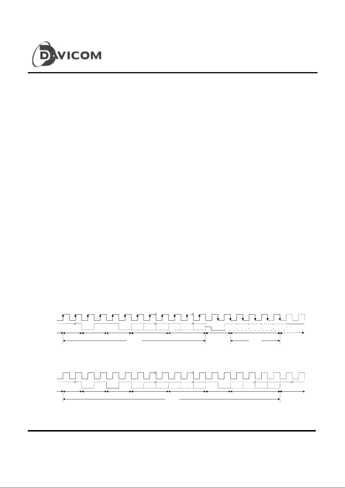
MII Serial Management Interface
The serial management interface uses a simple, twowired serial interface to obtain and control the status
of the physical layer through an MII interface (MDC
and MDIO pins). The Management Data Cl ock (MDC)
is equipped with a maximum clock rate of 2.5MHz,
while Management Data Input /Out put (MDIO) works
as a bi-directional, open-drain pi n shared by up to 32
devices.
DM9131’s management funct ions correspond to MII
specification for IEEE 802.3u-1995 (Clause 22) and
the registers 0 through 6 with vendor-specific
registers 11,15,16,17,18.
In read/write operation, the management data frame
is 64-bit long start with 32 cont iguous logic one bits
(preamble) synchronization clock cycles on MDC.
The S t art of Frame Delimite r (SFD ) is indicated by a
<01> pattern followed by the operation code
(OP):<10> indicates Read operation and <01>
indicat es Write operatio n. For read operation, a 2-bit
turnaround (TA) filing between Resistor Addres s f ield
and Data field is provided for MDIO to avoid
contention. “Z” stands for high im pedanc e state.
Following turnaround time, a 16-bit data is read from
or written onto management registers.
Management Interface - Read Frame Structure
32 "1"s
0110A4A3A0R4R3R0
Z
0
Idle Preamble SFD Op Code PHY Address Register Address Turn Around Data Idle
Read
Write
MDC
MDIO Read
D15 D14 D1 D0
/
/
/
/
Management Interface - Write Frame Structure
32 "1"s 0 1 10 A4 A3 A0 R4 R3 R0 1 0 D15 D14 D1 D0
Idle Preamble SFD Op Code PHY Address Register Address Turn Around Data Idle
Write
MDC
MDIO Write
Page 11

DM9131
10/100 Mbps Fast Ethernet Physical Layer Si ngle Chi p Transceiver
Final 11
Version: DM9131-DS-F01
April 7, 2000
MII Register Description
ADD Name 15 14 13 12 11 10 9 8 7 6 5 4 3 2 1 0
00 CONTROL Reset Loop
back
Speed
select
Auto-N
Enable
Power
Down
Isolate Restart
Auto-N
Full
Duplex
Coll.
Test
Reserved
01 STATUS T4
Cap.
TX FD X
Cap.
TX HDX
Cap.
10 FDX
Cap.
10 HDX
Cap.
Reserved Pream.
Supr.
Auto-N
Compl.
Remote
Fault
Auto-N
Cap.
Link
Status
Jabber
Detect
Extd
Cap.
02PHYID1000000011000000 0
03 PHYID2 1 0 1 1 1 0 Model No. Version No.
04 Auto-Neg.
Advertise
Next
Page
FLP Rcv
Ack
Remote
Fault
Reserved FC
AdvT4Adv
TX FD X
Adv
TX HDX
Adv
10 FDX
Adv
10 HDX
Adv
Advertised Protocol Selector Field
05 Link Part.
Ability
LP Next
PageLPAck
LP
RF
Reserved LP
FC
LP
T4LPTX FD XLPTX HDXLP10 FDXLP10 HDX
Link Partner Protocol Selector Field
06 Auto-Neg.
Expansion
Reserved Pardet
Fault
LP Next
Pg Able
Next Pg
Able
New Pg
Rcv
LP AutoN
Cap.
16 Aux.
Config.BP4B5BBPSCRBPALIGN
BP_AD
POK
Repeat
mode
TX/F X
Select
FEF
Enable
RMII
Enable
Force
100LNK
SPDLE
D_CTL
Rsvd FDXL E
D_CTL
Reset
St. Mch
Pream.
Supr.
Sleep
mode
Remote
LoopOut
17 Aux.
Conf/Stat
100
FDX
100
HDX10FDX
10 HDX Reserved PHY ADDR [4:0] Auto-N. Monitor Bit [3:0]
18 10T
Conf/Stat
Rsvd LP
Enable
HBE
Enable
SQUE
Enable
JAB
Enable
10T
Serial
Reserved Polarity
Reverse
21 MDINTR INTR
PEND
Rsvd Rsvd Rsvd FDX
Mask
SPD
Mask
Link
Mask
INTR
Mask
Rsvd Rsvd Rsvd FD X
Change
SPD
Change
Link
Change
INT
Enable
INTR
Status
22 Rcv Error
Counter
Receive Error Counter
23 Disconnect
Counter
Reserved Disconnect Counter
Key to Default
In the register description that follows, the default
column takes the form:
<Reset Value> , <Access Type> / <Att r ibute(s)>
Where
<Reset Value> :
1 Bit set t o l ogic one
0 Bit set t o l ogic zero
X No default value
(PIN#) Value latched in from pin # at reset
<Access Type>:
RO = Read onl y
RW = Read/Write
<Attribute (s)>:
SC = Self clearing
P = Value permanently set
LL = Latching low
LH = Latching high
Page 12

DM9131
10/100 Mbps Fast Ethernet Physical Layer Si ngle Chi p Transceiver
12 Final
Version: DM9131-DS-F01
April 7, 2000
Basic Mode Control Register (BMCR) - 00
Bit Bit Name Default Description
0.15 Reset 0, RW/SC
Reset:
1=Software reset
0=Normal operati on
This bit set s the status and controls the PHY registers to their
default states. This bit, which is self-clearing, will keep returning a
value of one until the reset pr oces s is completed
0.14 Loopback 0, RW
Loopback:
Loop-back control register
1 = Loop-back enabled
0 = Normal operation
When in 100Mbps operation mode, setting this bit may cause the
descrambler to lose synchronization and produce a 720ms "dead
time" before any valid data appear at the MII receive outputs
0.13 Speed selection 1, RW
Speed select:
1 = 100Mbps
0 = 10Mbps
Link speed may be selected either by this bit or by auto-negotiation.
When auto-negotiation is enabled and bit 12 is set, this bit will
return auto-negotiation selected media type.
0.12 Autonegotiation
enable
1, RW
Auto-negotiation enable:
1 = Auto-negotiation is enabl ed, bit 8 and 13 will be in autonegotiation status
0.11 Power down 0, RW
Power Down:
While in the power-down state, the PHY should respond to
management transactions. During the transition to power-down
state and while in the power-down state, the PHY should not
generate spurious signals on the MII.
1=Power down
0=Normal operati on
0.10 Isolate 0,RW
Isolate:
1 = Isolates the DM9131 from the MII with the exception of the
serial management. (When this bit is asserted, the DM9131 does
not respond to the TXD[0:3], TX_EN, and TX_ER inputs, and it
shall present a high impedance on its TX_CLK, RX_CLK, RX_DV,
RX_ER, RX[0:3], CO L and CRS outputs. When PHY is isolated
from the MII it shall respond to the management transactions)
0 = Normal operation
0.9 Restart autonegotiation
0,RW/SC
Restart auto-negotiation:
1 = Restart auto-negot iation. Re-ini t iates the auto-negotiation
process. W hen auto-negotiation is disabled (bit 12 of this register
cleared), this bit has no function and it should be cleared. This bit is
self-clearing and it will keep returning a value of 1 until autonegotiation is initiated by the DM9131. The operation of the autonegotiation process will not be affected by the management entity
that clear s t his bit
0 = Normal operation
Page 13

DM9131
10/100 Mbps Fast Ethernet Physical Layer Si ngle Chi p Transceiver
Final 13
Version: DM9131-DS-F01
April 7, 2000
0.8 Duplex mode 1, RW
Duplex mode:
1 = Full duplex operation. Duplex selection is allowed when Autonegotiation is disabled (bit 12 of this register is cleared). With
auto-negotiation enabled, this bit reflects the duplex capability
selected by auto-negotiation
0 = Normal operation
0.7 Collision t est 0,RW
Collision test:
1 = Collision test enabled. When set, this bit will cause t he C O L
signal to be asserted in response to the assertion of TX_EN
0 = Normal operation
0.6-0.0 Reserved 0,RO
Reserved:
Write as 0, ignore on read
Basic Mode Status Register (BMSR) - 01
Bit Bit Name Default Description
1.15 100BASE-T4 0,RO/P
100BASE-T4 capable:
1 = DM9131 is able to perform in 100BASE-T4 mode
0 = DM9131 is not able to perform in 100BASE-T4 mode
1.14 100BASE-TX
full duplex
1,RO/P
100BASE-TX full duplex capable:
1 = DM9131 is able to perform 100BASE-TX in full duplex mode
0 = DM9131 is not able to perform 100BASE-TX in full duplex mode
1.13 100BASE-TX
half dupl ex
1,RO/P
100BASE-TX half duplex capable:
1 = DM9131 is able to perform 100BASE-TX in half duplex mode
0 = DM9131 is not able to perform 100BASE-TX in half duplex
mode
1.12 10BASE-T
full duplex
1,RO/P
10BASE-T fu ll dup lex capable:
1 = DM9131 is able to perform 10BASE-T in full duplex mode
0 = DM9131 is not able to perform 10BASE-TX in full duplex mode
1.11 10BASE-T
half dupl ex
1,RO/P
10BASE-T half duplex capable:
1 = DM9131 is able to perform 10BASE-T in half duplex mode
0 = DM9131 is not able to perform 10BASE-T in half duplex mode
1.10-1.7 Reserved 0,RO
Reserved:
Write as 0, ignore on read
1.6 MF preamble
suppression
0,RO
MII frame preamble suppression:
1 = PHY w ill acce p t management frames with preamble suppressed
0 = PHY will not accept management f r ames with preamble
suppressed
1.5 Auto-
negotiation
Complete
0,RO
Auto-negotiation complete:
1 = Auto-negotiation process completed
0 = Auto-negotiation process not completed
1.4 Remote fault 0,
RO/LH
Remote fault:
1 = Remote fault condition detected (cleared on read or by a chip
reset). Fault criteria and detection method is DM9131
implementation specific. This bit will set after the RF bit in the
ANLPAR (bit 13, register address 05) is set
0 = No remote fault condition detected
1.3 Auto-
negotiation
ability
1,RO/P
Auto configuration ability:
1 = DM9131 is able to perform auto-negotiation
0 = DM9131 is not able to perform auto-negotiation
1.2 Link status 0,RO/LL
Link status:
Page 14

DM9131
10/100 Mbps Fast Ethernet Physical Layer Si ngle Chi p Transceiver
14 Final
Version: DM9131-DS-F01
April 7, 2000
1 = Valid link is established (for either 10Mbps or 100Mbps
operation)
0 = Link is not established
The link status bit is implemented with a latching function, so that
the occurrence of a link failure condition cau ses the link status bit to
be cleared and remain cleared until it is read via the management
interface
1.1 Jabber detect 0,
RO/LH
Jabber detect:
1 = Jabber condition detected
0 = No jabber
This bit is implemented with a latching function. Jabber conditions
will set this bit unle ss it is cleared by a read to this register through a
management interface or a DM9131 reset. This bit works only in
10Mbps mode
1.0 Extended
capability
1,RO/P
Extended capability:
1 = Extended register capable
0 = Basic register capable only
PHY ID Identifier Register #1 (PHYID1) - 02
The PHY Identifier Registers #1 and #2 work together in a single identifier of th e DM9131. The Identifi er consists
of a concatenation of the Organizationally Unique Identifier (OUI), a vendor's model number, and a model
revision number. DAVICOM Semiconductor's IEEE assigned OUI is 00606E.
Bit Bit Name Default Description
2.15-2.0 OUI_MSB <0181h>
OUI most significant bits:
This register stores bit 3 to 18 of the OUI (00606E) to bit 15 to 0 of
this register respe ctively. The most significant two bits of the OUI
are ignored (the IEEE standard refers to these as bit 1 and 2)
PHY Identifier Register #2 (PHYID2) - 03
Bit Bit Name Default Description
3.15-3.10 OUI_LSB <101110>,
RO/P
OUI least significant bits:
Bit 19 to 24 of the OUI (00606E) are mapped to bit 15 to 10 of this
register respectively
3.9-3.4 VNDR_MDL <000010>,
RO/P
Vendor mod el numb er:
Six bits of vendor model number mapped to bit 9 to 4 (most
signif icant bi t to bit 9)
3.3-3.0 MDL_REV <0000>,
RO/P
Model revision number:
Four bits of vendor model revision number mapped to bit 3 to 0
(most signifi cant bit to bit 3)
Page 15

DM9131
10/100 Mbps Fast Ethernet Physical Layer Si ngle Chi p Transceiver
Final 15
Version: DM9131-DS-F01
April 7, 2000
Auto-negotiation Advertisement Register(ANAR) - 04
This register contains the advert ise d abilities of this DM9131 device as they will be transmitted to its link partner
during Auto-negotiation.
Bit Bit Name Default Description
4.15 NP 0,RO/P
Next page indication:
0 = No next page available
1 = Next page available
The DM9131 has no next page, so this bit is permanently set to 0
4.14 ACK 0,RO
Acknowledge:
1 = Link partner ability data reception ackn owledged
0 = Not acknowledged
The DM9131's auto-negotiation state machine will automatically
control this bit in the outgoing FLP bursts and set it at the
appropriate time during the auto-negotiation process. Software
should not attempt to write to this bit.
4.13 RF 0, RW
Remote fault:
1 = Local device senses a fault condition
0 = No fault detected
4.12-4.11 Reserved X, RW
Reserved:
Write as 0, ignore on read
4.10 FCS 0, RW
Flow control support:
1 = Controller chip supports flow control ability
0 = Controller chip doesn’t support flow contr ol ability
4.9 T4 0, RO/P
100BASE-T4 support:
1 = 100BASE-T4 is supported by the local device
0 = 100BASE-T4 is not supported
The DM9131 does not support 100BASE-T4 so this bit is
permanently set to 0
4.8 TX_FDX 1, RW
100BASE-TX full duplex support:
1 = 100BASE-TX full duplex is supported by the local device
0 = 100BASE-TX full duplex is not supported
4.7 TX_HDX 1, RW
100BASE-TX support:
1 = 100BASE-TX is supported by the local device
0 = 100BASE-TX is not supported
4.6 10_FDX 1, RW
10BASE-T full duplex support:
1 = 10BASE-T full duplex is supported by the local device
0 = 10BASE-T ful l duplex is not supported
4.5 10_HDX 1, RW
10BASE-T support:
1 = 10BASE-T is supported by the local device
0 = 10BASE-T is not supported
4.4-4.0 Selector <00001>, RW
Protocol selection bits:
These bits contain the binary encoded protocol selector supported
by this node.
<00001> indicates that this device supports IEEE 802.3 CSMA/CD.
Page 16

DM9131
10/100 Mbps Fast Ethernet Physical Layer Si ngle Chi p Transceiver
16 Final
Version: DM9131-DS-F01
April 7, 2000
Auto-negotiation Link Partner Ability Register (ANLPAR) – 05
This register contains the advert ise d abilities of the li nk partner When received during Auto-negotiation.
Bit Bit Name Default Description
5.15 NP 0, RO
Next page indication:
0 = Link partner, no next page available
1 = Link partner, next page available
5.14 ACK 0, RO
Acknowledge:
1 = Link partner ability data reception ackn owledged
0 = Not acknowledged
The DM9131's auto-negotiation state machine will automatically
control this bit from the incoming FLP bursts. Software should not
attempt to w r ite to this bit.
5.13 RF 0, RO
Remote Fault:
1 = Remote fault indicated by link partner
0 = No remote fault indicated by link partner
5.12-5.11 Reserved X, RO
Reserved:
Write as 0, ignore on read
5.10 FCS 0, RW
Flow control support:
1 = Controller chip supports flow control ability by link partner
0 = Controller chip doesn’t support flow contr ol ability by link
partner
5.9 T4 0, RO
100BASE-T4 support:
1 = 100BASE-T4 is supported by the link partner
0 = 100BASE-T4 is not supported by the link partner
5.8 TX_FDX 0, RO
100BASE-TX full duplex support:
1 = 100BASE-TX full duplex is supported by the link partner
0 = 100BASE-TX full duplex is not supported by the link partner
5.7 TX_HDX 0, RO
100BASE-TX support:
1 = 100BASE-TX half duplex is supported by the link partner
0 = 100BASE-TX half duplex is not supported by the link partner
5.6 10_FDX 0, RO
10BASE-T full duplex support:
1 = 10BASE-T full duplex is supported by the link partner
0 = 10BASE-T full duplex is not supported by the link partner
5.5 10_HDX 0, RO
10BASE-T support:
1 = 10BASE-T half duplex is supported by the link partner
0 = 10BASE-T half duplex is not supported by the link partner
5.4-5.0 Selector <00000>, RO
Protocol selection bits:
Link partner’s binary encoded protocol selector
Page 17

DM9131
10/100 Mbps Fast Ethernet Physical Layer Si ngle Chi p Transceiver
Final 17
Version: DM9131-DS-F01
April 7, 2000
Auto-negotiation Expansion Register (ANER)- 06
6.15-6.5 Reserved X, RO
Reserved:
Write as 0, ignore on read
6.4 PDF 0, RO/LH
Local device parallel detection fault:
PDF = 1 : A fault detected via parallel detection function.
PDF = 0 : No fault detected via parallel detection function
6.3 LP_NP_ABLE 0, RO
Link partne r next page able:
LP_NP_ABLE = 1 : Link partner, next page available
LP_NP_ABLE = 0 : Link partner, no next page
6.2 NP_ABLE 0,RO/P
Local device next page able:
NP_ABLE = 1 : DM9131, next page available
NP_ABLE = 0 : DM9131, no next page
DM9131 does not support this function, so this bit is always 0.
6.1 PAGE_RX 0, RO/LH
New page received:
A new link code word page received. This bit will be automatically
cleared when the register (register 6) is read by management.
6.0 LP_AN_ABLE 0, RO
Link partne r auto-negot iation able:
A “1” in thi s bi t indic ates that the link partner supports Autonegotiation.
DAVICOM Specified Conf igurati on Regist er (DSCR) - 16
Bit Bit Name Default Description
16.15 BP_4B5B (Pin#xx), RW
Bypass 4B5B encoding and 5B4B decoding :
The value of the BP4B5B pin(xx) is latched into this bit at powerup/reset.
1 = 4B5B encoder and 5B4B decoder function bypassed
0 = Normal 4B5B and 5B4B operation
16.14 BP_SCR 0, RW
Bypass scrambler/descrambler function :
1 = Scrambler and descrambler function bypassed
0 = Normal scrambler and descrambler operation
16.13 BP_ALIGN 0, RW
Bypass symbol alignment function:
1 = Receive funct ions (descrambl er , symbol alignment and
symbol dec oding functions) bypassed. Transmi t functions
( symbol encoder and scrambler) bypassed
0 = Normal operation
16.12 BP_ADPOK 0, RW
BYPASS ADPOK :
Force signal detector (SD) active. This register is for debug only,
not release to customer.
1=Force SD is OK,
0=Normal operati on
16.11 REPEATER (Pin#xx),RW
Repeat er/Node mode :
The value of the Repeater/Node pin(xx) is latched into this bit at
power-up/reset.
1 = Repeater mode
0 = Node mode
16.10 T X 1, RW
100BASE-TX or FX mode control:
1 = 100BASE-TX operation
0 = 100BASE-FX operation
Page 18

DM9131
10/100 Mbps Fast Ethernet Physical Layer Si ngle Chi p Transceiver
18 Final
Version: DM9131-DS-F01
April 7, 2000
16.9 FEF 0, RW
Far End Fault enable :
Control the Far End Fault mechanism associated with 100Base-FX
operation.
1 = Enable
0 = Disable
16.8 RMII_Enable (Pin#xx), RW
Reduced MI I enable :
Select normal M II or reduced MII. The value of the RMII pin(xx) is
latched int o this bit at power-up/reset.
0 = Normal MII
1 = Enable Reduced MII
16.7 F_LINK_100 0, RW
Force good link in 100Mbps:
0 = Normal 100Mbps operation
1 = Force 100Mbps good link status
This bit is useful for diagnostic purposes.
16.6 SPLED_CTL 0, RW
Speed LED Disable :
0 : Normal SPEEDLED output to indicate speed status
1 : Disable SPEEDLED output and enable SD signal monitor (for
internal debug). W hen this bit is set, i t control t he SPEEDLED as
100BASE-X SD (not fiber mode) signal output .For debug only.
16.5 Reserv ed 0, RO
Reserved
16.4 FDXLED_CTL 0,RW
Full-duplex LED mode select :
0 = FDXLED output is configured to indicate full-duplex status
1 = COLLED output is configured to indicate the presence of
collision activity operation.
16.3 SMRST 0, RW
Reset state machine:
When writes 1 to this bit, all state machines of PHY will be reset.
This bit is self- c lear after reset is completed.
16.2 MFPSC 0, RW
MF preamble suppression control:
MII frame preamble suppression control bit
1 = MF preamble suppression bit on
0 = MF preamble suppression bit off
16.1 SLE E P 0, RW
Sleep mod e:
Writing a 1 to this bit will cause PHY entering the Sleep mode and
power down all circ ui t except oscillator and clock generator circuit.
When waking up from Sleep mode (write this bit to 0), the
config urat ion will go b ack to the state before sleep; but the state
machine will be reset
16.0 RLOUT 0, RW
Remote loopout c ont rol:
When this bit is set to 1, the received data will loop out to the
transmi t channel. T his is useful for bit error rate testing
Page 19
DM9131
10/100 Mbps Fast Ethernet Physical Layer Si ngle Chi p Transceiver
Final 19
Version: DM9131-DS-F01
April 7, 2000
DAVICOM Specified Conf igurati on and S t at us Register (DSCSR) - 17
Bit Bit Name Default Description
17.15 100FDX 1, RO
100M full duplex operation mode:
After auto-negotiation is completed, results will be written to this bit.
If this bit is 1, it means the operat ion 1 mode is a 100M full duplex
mode. The software can read bit[15:12] to see which mode is
selected after auto-negotiation. This bit is invalid when it is not in
the auto-negotiation mode.
17.14 100HDX 1, RO
100M half duplex operation mode:
After auto-negotiation is completed, results will be written to this bit.
If this bit is 1, it means the operat ion 1 mode is a 100M half duplex
mode. The software can read bit[15:12] to see which mode is
selected after auto-negotiation. This bit is invalid when it is not in
the auto-negotiation mode.
17.13 10FDX 1, RO
10M full duplex operation mode:
After auto-negotiation is completed, results will be written to this bit.
If this bit is 1, it means the operat ion 1 mode is a 10M Full Duple x
mode. The software can read bit[15:12] to see which mode is
selected after auto-negotiation. This bit is invalid when it is not in
the auto-negotiation mode.
17.12 10HDX 1, RO
10M half duplex operation mode:
After auto-negotiation is completed, results will be written to this bit.
If this bit is 1, it means the operat ion 1 mode is a 1 0M half duplex
mode. The software can read bit[15:12] to see which mode is
selected after auto-negotiation. This bit is invalid when it is not in
the auto-negotiation mode.
17.11-
17.9
Reserved 0, RO
Reserved:
Write as 0, ignore on read
17.8-17.4 PHYADR[4:0] (PHYADR),
RW
PHY address Bit 4:0:
The first PHY add ress bit tr ansmitted or receive d is the MSB of the
address (bit 4). A station management entity connected to multiple
PHY entities m ust know the appropriate address of each PHY.
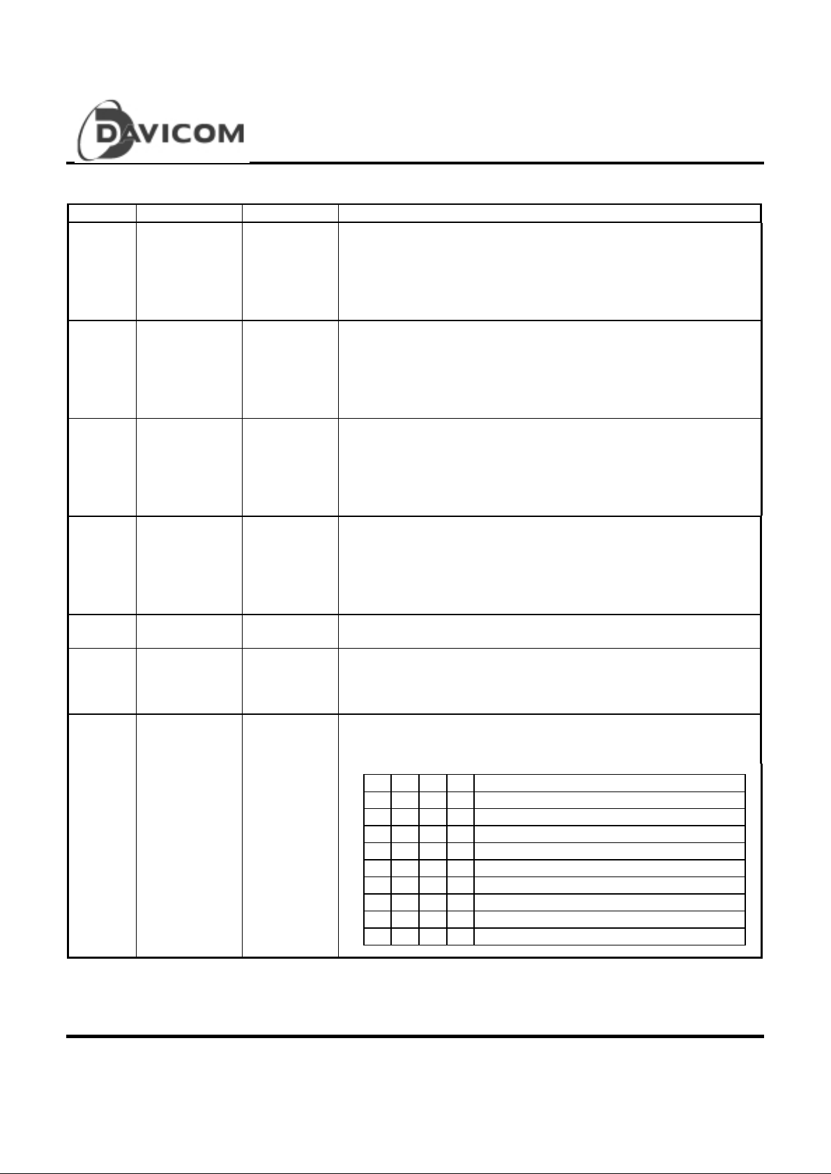
17.3-17.0 ANMB [3:0] 0, RO
Auto-negotiation monitor bits:
These bits are for debug only. The auto-negotiation status will be
written to these bits.
b3 b2 b1 b0
0 0 0 0 In IDLE state
0 0 0 1 Ability match
0 0 1 0 Acknowledge match
0 0 1 1 Acknowledge match fail
0 1 0 0 Consistency match
0 1 0 1 Consistency match fail
0 1 1 0 Parallel det ec t s signal_link_ready
0 1 1 1 Parallel det ec t s signal_link_ready f ail
1 0 0 0 Auto-negotiation completed successfully
Page 20

DM9131
10/100 Mbps Fast Ethernet Physical Layer Si ngle Chi p Transceiver
20 Final
Version: DM9131-DS-F01
April 7, 2000
10BASE-T Configuration/Status (10BTCSR) - 18
Bit Bit Name Default Description
18.15 Reserved 0, RO
Reserved:
Write as 0, ignore on read
18.14 LP _E N 1, RW
Link pulse enable :
1 = Transmission of link pulses enabled
0 = Link pulses disabled, good l ink condition forced
This bit is valid only in 10Mbps operation.
18.13 HBE 1,RW
Heartbeat enab le:
1 = Heartbeat function enabled
0 = Heartbeat function disabled
When the DM9131 is configured for full duplex operation, this bit will
be ignored (the collision/heartbeat function is invalid in full duplex
mode).
18.12 SQUELCH 1, RW
Squelch enable :
1 = normal squelch
0 = low squelch
18.11 JABEN 1, RW
Jabber Enable:
Enables or disables the Jabber function when the DM9131 is in
10BASE-T ful l duplex or 10BASE-T transceiver loopback mode
1 = Jabber function enabled
0 = Jabber function disabled
18.10 10BT_SER 0,RW
10BASE-T serial mode:
1 = 10BASE-T serial mode selected
0 = 10BASE-T nibble mode selected
Serial mode is not supported for 100Mbps operation.
18.9-18.1 Reserved 0, RO
Reserved:
Write as 0, ignore on read
18.0 POLR 0, RO
Polarity reversed:
When this bit is set to 1, it indicates that the 10Mbps cable polarity is
reversed. This bit is set and cleared by 10BASE-T module
automatically.
Page 21

DM9131
10/100 Mbps Fast Ethernet Physical Layer Si ngle Chi p Transceiver
Final 21
Version: DM9131-DS-F01
April 7, 2000
DAVICOM Specified Interrupt Register – 21
Bit Bit Name Default Description
21.15 INTR PEND 0, RO
Interrupt pending :
Indicates that the interr upt is pending and is cleared by the current
read. This bit shows the same result as bit 0. (I NTR Status)
21.14-
21.12
Reserved 0, RO
Reserved
21.11 FDX mask 1, RW
Full-duplex interrupt mask :
When this bit is set, the Duplex status change will not generate the
interrupt
21.10 SPD mask 1, RW
Speed in t errupt mask :
When this bit i s set, the Speed status change will not generate the
interrupt
21.9 LINK mask 1, RW
Link interrupt mask :
When this bit i s set, the link status change will not generate the
interrupt
21.8 INTR mask 1, RW
Master interrupt mask :
When this bit i s set, no interrupts will be generated under any
condition.
21.7-21.5 Reserved 0, RO
Reserved
21.4 FDX change 0,RO/ LH
Duplex status c ha nge int errupt :
“1” indicates a change of duplex since last register read. A read of
this register will clear this bit.
21.3 SPD change 0, RO/LH
Speed status change interrupt :
“1” indicates a change of speed since last register read. A read of
this register will clear this bit.
21.2 LINK change 0, RO/LH
Link status change interrupt :
“1” indicates a change of link since last register read. A read of this
register will clear this bit.
21.1 INTR enable 0, RW
Interrupt enable :
“1” = enable the interrupt mode,
“0” = disable
21.0 INTR status 0, RO/LH
Interrupt status :
The status of MDINTR# . “1” indicates that the interrupt mask is off
that one or more of the change bits are set. A read of this register
will clear this bit.
DAVICOM Specified Receive Error Counter Re gister (RECR) – 22
Bit Bit Name Default Description
22.15-0 Rcv_Er r _Cnt 0, RO
Receive error counter :
Receive error counter that increments upon detection of REER
DAVICOM Specified Disconnect Counter Register (DISCR) – 23
Bit Bit Name Default Description
23.15-
23.8
Reserved 0, RO
Reserved
23.7-23.0 Disconnect
Counter
0, RO Disconnect Count er t hat increments upon detection of
disconnection.
Page 22
DM9131
10/100 Mbps Fast Ethernet Physical Layer Si ngle Chi p Transceiver
22 Final
Version: DM9131-DS-F01
April 7, 2000
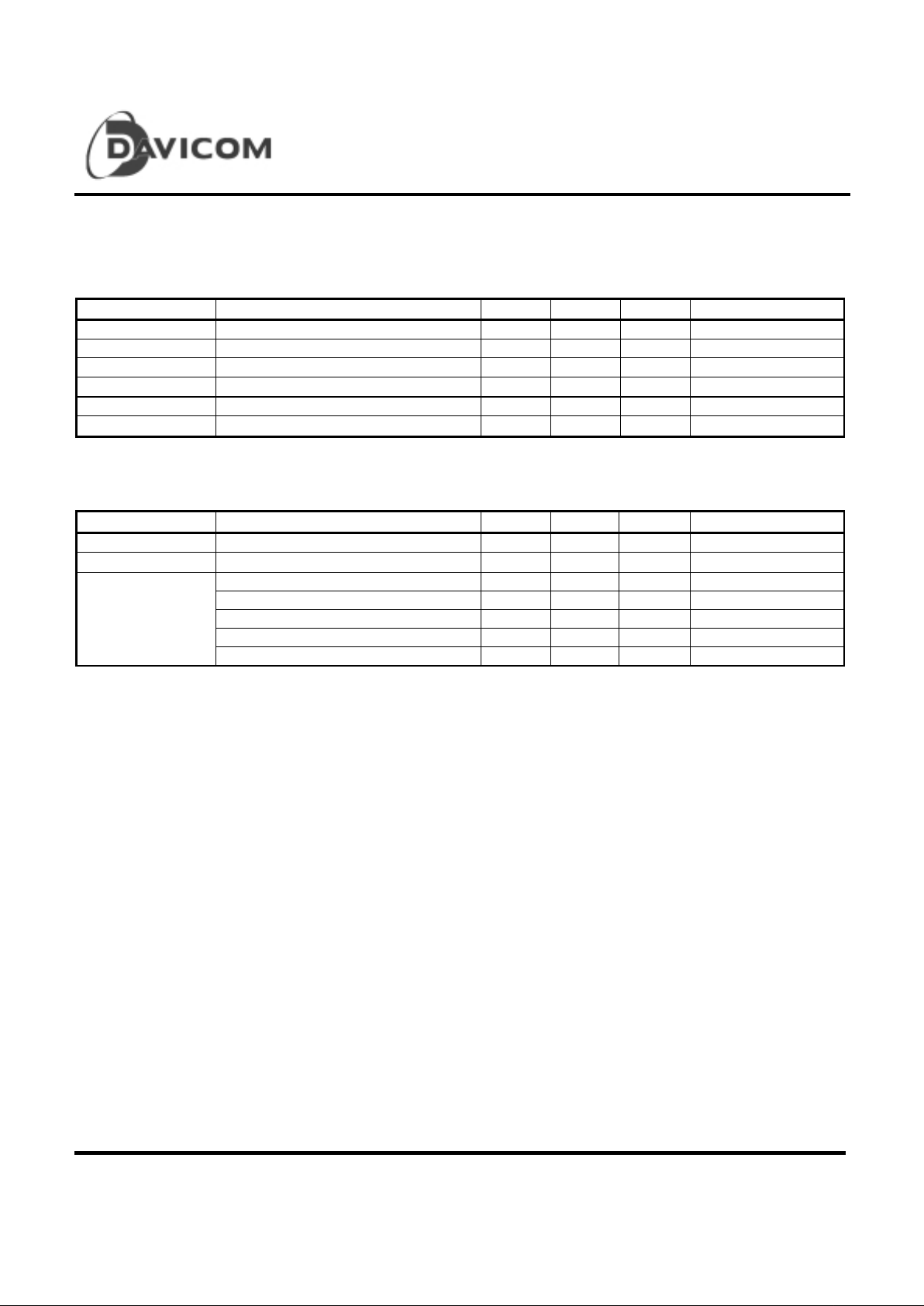
Absolute Maximum Ratings
Absolute Maximum Ratings ( 25°°°°C )
Symbol Param ete r Min. Max . Unit Conditions
D
VCC, AVCC
Supply Voltage -0.3 3.6 V
V
IN
DC Input Voltage (VIN)-0.55.5V
V
OUT
DC Output Voltage(V
OUT
)-0.33.6V
T
stg
Storage Temperature Rang (T
stg
) -40 +125
°C
P
D
Power Dissipation (PD) --- 0.43 W
L
T
Lead Temp. (TL, Soldering, 10 sec.) --- 240
°C
Operating C onditions
Symbol Para me ter Min. Max. Unit Conditions
D
VCC,AVCC
Supply Voltage 3.135 3.465 V
Tc Case Temperature --- 85
°C
100BASE-TX --- 115 m
A
3.3V
100BASE-FX --- 25 m
A
3.3V
10BASE-T TX --- 125 m
A
3.3V
10BASE-T idle --- 44 m
A
3.3V
P
D
(Power Dissipation)
Auto-negotiation --- 76 m
A
3.3V
Comments
Stresses above those listed under “Absolute
Maximum Ratings” may cause permanent damage to
the device. These are stress ratings only.
Functional operation of this device at these or any
other conditions above those indicated in the
operational sections of this specification is not
implied. Exposure to absolute maximum rating
conditions for extended periods may affect device
reliability.
Page 23
DM9131
10/100 Mbps Fast Ethernet Physical Layer Si ngle Chi p Transceiver
Final 23
Version: DM9131-DS-F01
April 7, 2000
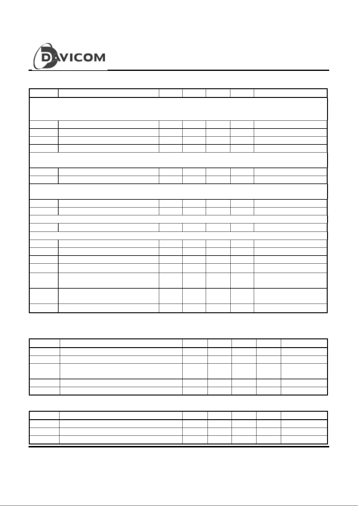
DC Electrical Ch aracteristics
(VCC = 3.3V)
Symbol Param ete r Min. Typ. Max. Unit Conditions
TTL Inputs
(TXD0 ~TXD 3, TX CL K, MD C, MDIO, TX E N, TX ER, R XE N, TESTM ODE, R MII, OSCS EL, PH YAD 0~4, OP MODE0 -2,
RPTR, BP4B5B, RESET# )
V
IL
Input Low Voltage --- --- 0.8 V
V
IH
Input High Voltage 2.0 --- --- V
I
IL
Input Low Leakage Current --- --- 10 u
A
VIN = 0.4V
I
IH
Input High Leakage Current --- --- -10 u
A
V
IN
= 2.7V
MII TTL Outputs
( RXD0-RXD3, RXDV, RXER, CRS, COL, MDIO)
V
OL
Output Low Voltage --- --- 0.4 V IOL = 4m
A
V
OH
Output High Voltage 2.4 --- --- V I
OH
= -4m
A
Non-MII TTL Outputs
(LINKLED#, SPEEDLED#, FDX LED#, MDINTR#)
V
OL
Output Low Voltage --- --- 0.4 V I
OL
= 1m
A
V
OH
Output High Voltage 2.4 --- --- V IOH = -0.1m
A
Receiver
V
ICM
RX+/RX- Common mode Input Voltage --- 0.9 --- V
100 Ω Termination Across
Transmitter
VTD100 100TX+/- Differential Output Voltage 1.9 2.0 2.1 V Peak to Peak
VTD10 10TX+/- Differential Output Voltage 4.4 5 5.6 V Peak to Peak
ITD100 100TX+/- Differential Output Current • 19• • 20• • 21• m
A
ITD10 10TX+/- Differential Output Current • 44• • 50• • 19• m
A
V
OH
PECL Output Voltage – High V
CC-
1.05
V
CC
-
0.88
V
V
OL
PECL Output Voltage – Low V
CC-
1.81
V
CC-
1.62
V
IFD100 100FX+/- Differential Output Current • 17• • 18• • 19• m
A
AC Electr ical Char acteristics & Timing Wav eforms
TP Interface
Symbol Param ete r Min. Typ. Max. Unit Conditions
t
TR/F
100TX+/- Differential Rise/Fall Time 3.0 --- 5.0 ns
t
TM
100TX+/- Differential Rise/Fall Time Mismatch 0 --- 0.5 ns
t
TDC
100TX+/- Differential Output Duty Cycle
Distortion
0 --- 0.5 ns
t
T/T
100TX+/- Differential Output Peak-to-Peak Jitter 0 --- 1.4 ns
XOST 100TX+/- Differential Voltage Overshoot 0 --- 5 %
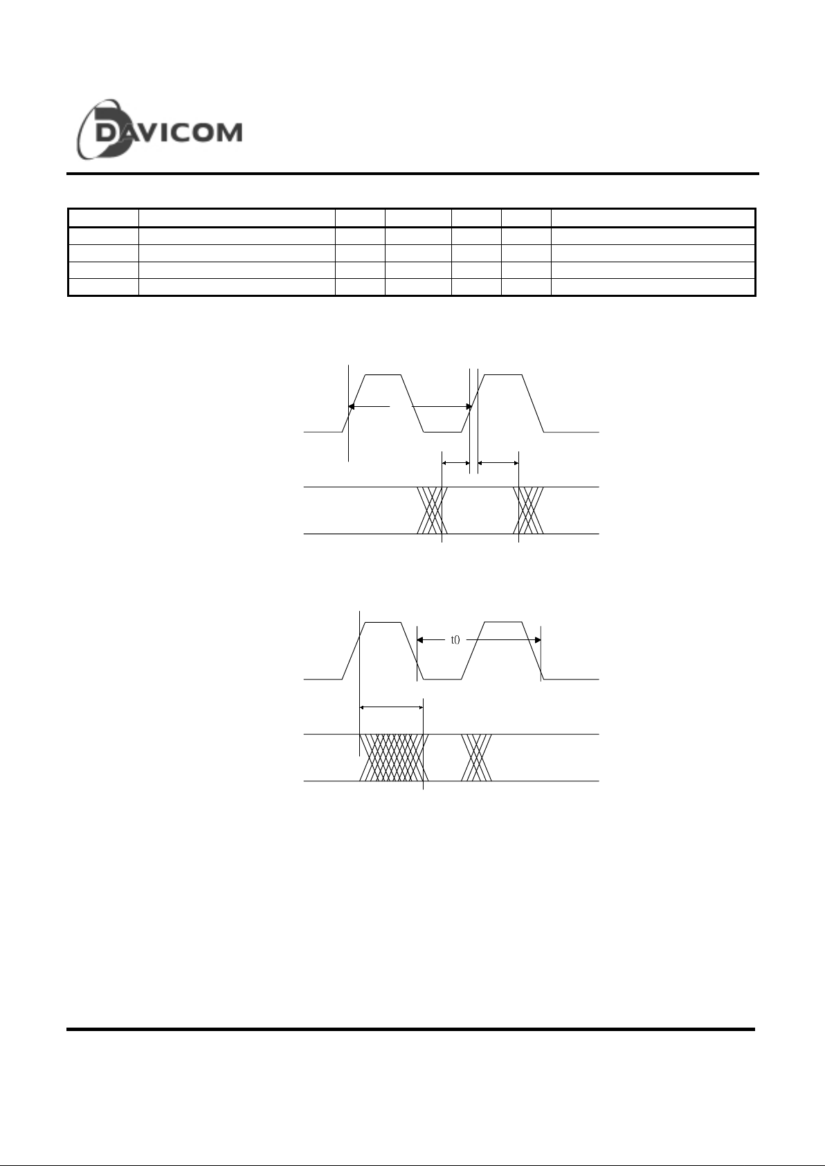
Oscillator /Cry sta l Timing
Symbol Param ete r Min. Typ. Max. Unit Conditions
t
CKC
OSC Cycle Time 39.998 40 40.002 ns 50ppm
t
PWH
OSC Pulse Width High 16 20 24 ns
t
PWL
OSC Pulse Width Low 16 20 24 ns
Page 24
DM9131
10/100 Mbps Fast Ethernet Physical Layer Si ngle Chi p Transceiver
24 Final
Version: DM9131-DS-F01
April 7, 2000
MDC/MDIO Timi ng
Symbol Paramete r Min. Typ. Max . Unit Conditions
t
0
MDC Cycle Time 80 --- --- ns
t
1
MDIO Setup Before MDC 10 --- --- ns When OUTPUT By STA
t
2
MDIO Hold After MDC 10 --- --- ns When OUTPUT By STA
t
3
MDC To MDIO Output Delay 0 --- 300 ns When OUTPUT By DM9131
MDIO timing when OUTPUT by STA
MDC
t
1
MDIO
10ns
(Min)
t
2
10ns
(Min)
t0
MDIO timing when OUTPUT by DM9131
MDC
t
3
MDIO
0 - 300 ns
Page 25
DM9131
10/100 Mbps Fast Ethernet Physical Layer Si ngle Chi p Transceiver
Final 25
Version: DM9131-DS-F01
April 7, 2000
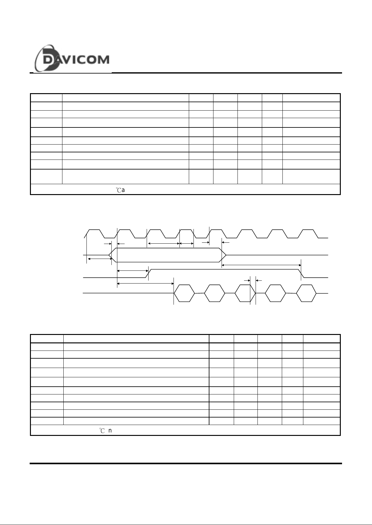
100BASE-TX Transmit Timing Parameters
Symbol Pa ram ete r Min. Typ. Max. Unit Conditions
t
TXc
TXCLK Cycle Time 39.996 40 40.004 ns
t
TXh
, t
TXl
TXCLK High/Low Time 16 20 24 ns
t
TX
s
TXD[0:3], TXEN, TXER Setup To TXCLK High 15 --- --- ns
t
TX
h
TXD[0:3], TXEN, TXER Hold From TXCLK High 15 --- --- ns
t
TXOD
TXCLK to Outp ut De lay 25 ns
t
1
TXEN Sampled To CRS Asserted --- 4 --- BT
t
2
TXEN Sampled To CRS De-as serted --- 4 --- BT
t
TX
pd
TXEN Sampled To TX+/- Out(Tx Latency) --- 8 --- BT
t
TX
r/f
100TX Driver Rise/Fall Time 3 4 5 ns 90% To 10%, Into
100ohm Differential
1
. Typical values are at 25and are for design aid only; not guaranteed and not subject to production testing.
100BASE-TX Transmit Timing Diagram
TXCLK
t
TX
h
t
2
t
TX
S
t
1
t
TX
pd
t
TX
r/f
TXD [0:3],
TXEN, TXER
CRS
100TX+/-
tTXc tTXh
tTXOD
100BASE-TX Receive Timing Parameter
Symbol Param ete r Min. Typ. Max. Unit Conditions
t
RXc
RXCLK Cycle Time 39.996 40 40.004
t
RXh, tRXl
RXCLK High/Low Time 16 20 24
t
RX
s
RXD[0:3), RXDV, RXER Setup To RXCLK High 10 - - ns
t
RX
h
RXD[0:3], RXDV, RXER Hold From RXCLK High 10 - - ns
t
RX
pd
RX+/- In To RXD[0:3] Out (Rx Latency) - 15 - BT
t
1
CRS Asserted To RXD[0:3], RXD V, RX ER - 4 - BT
t
2
CRS De-asserted To RXD[0:3], RXDV, RXER - 0 - BT
t
3
RX+/- In To CRS Asserted 10 - 14 BT
t
4
RX+/- Quiet To CRS De-asserted 14 - 18 BT
t
5
RX+/- In To COL De-Asserted 14 - 18 BT
1
. Typical values are at 25and are for design aid only; not guaranteed and not subject to production testing.
Page 26
DM9131
10/100 Mbps Fast Ethernet Physical Layer Si ngle Chi p Transceiver
26 Final
Version: DM9131-DS-F01
April 7, 2000
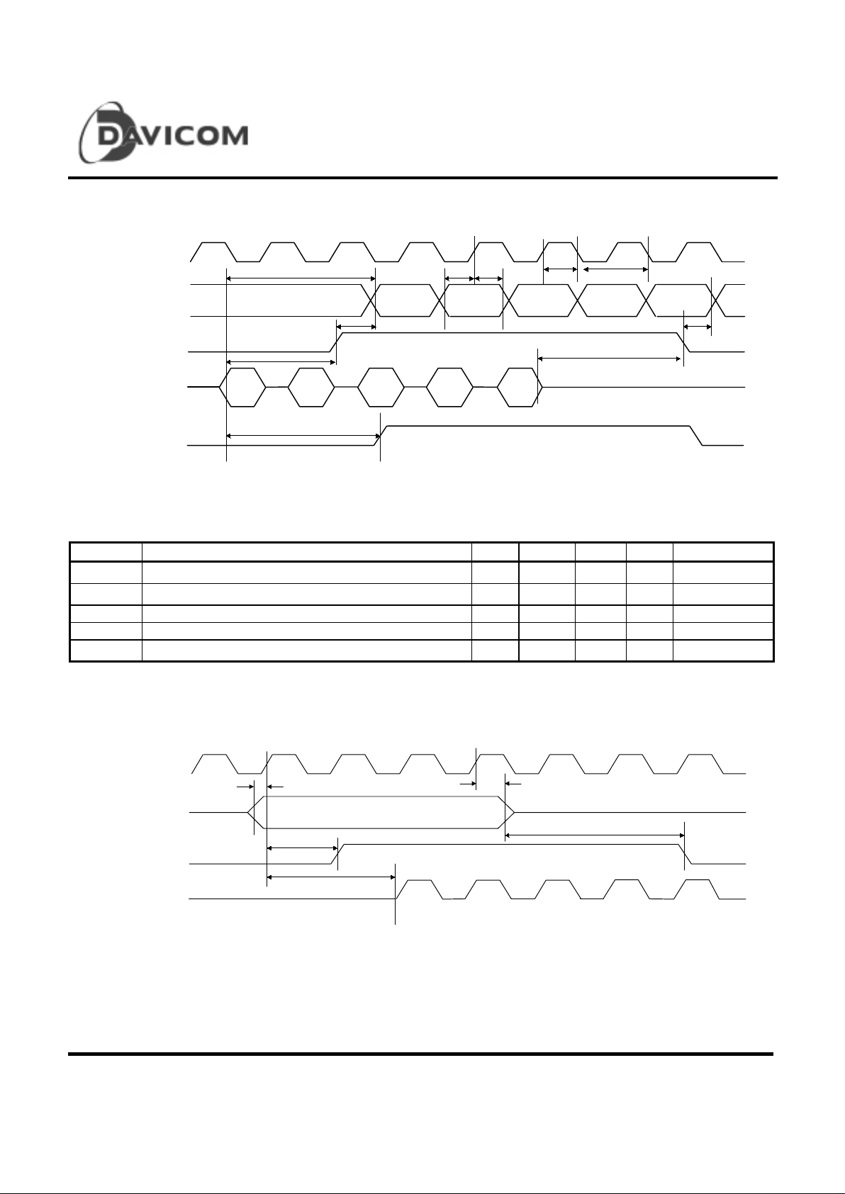
MII 100BASE-TX Receive Ti ming Diagram
RXCLK
t
2
t
1
t
TX
pd
RXD [0:3],
RXDV, RXER
CRS
RX+/-
t
RX
S
t
RX
h
t
4
t
3
COL
t
5
t
5
tRXctRXh
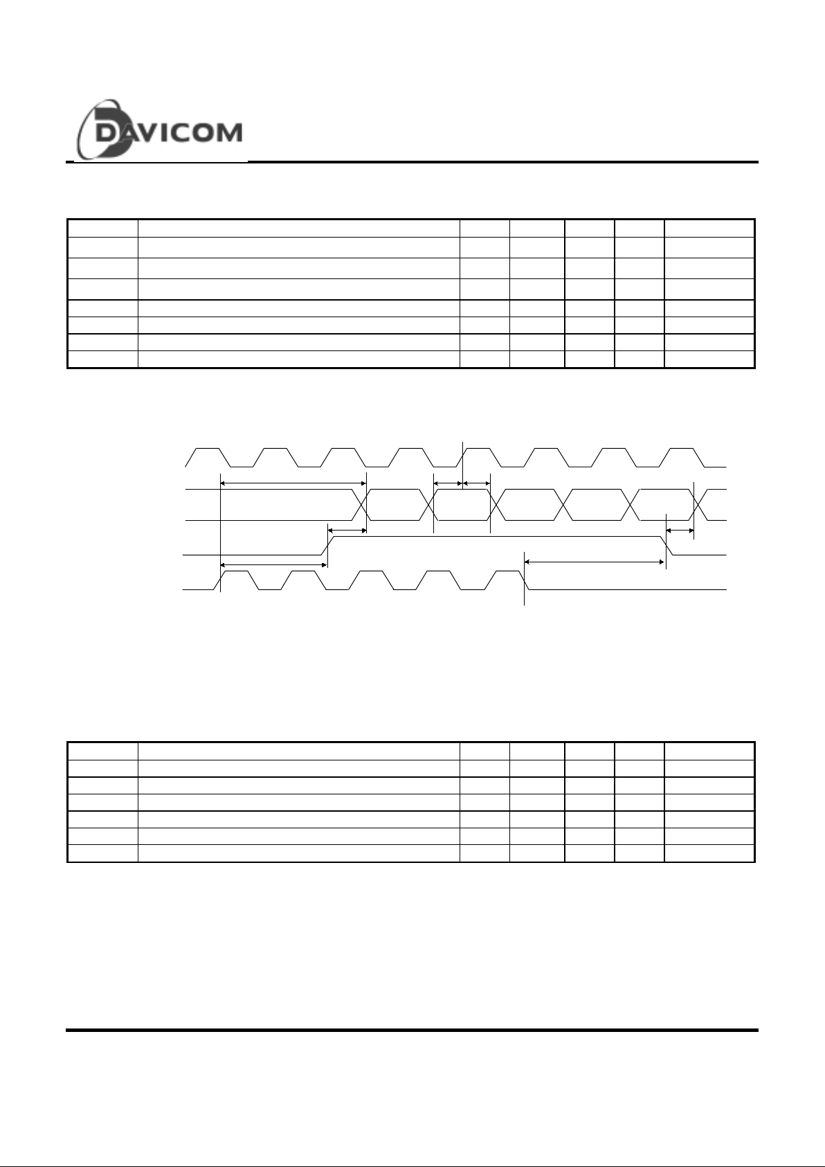
MII 10BASE-T Nibble Transmi t Timin g Parameters
Symbol Parame ter Min. Typ. Max. Unit Conditions
T
TX
s
TXD[0:3), TXEN, TXER Setup To TXCLK High 5 --- --- ns
T
TX
h
TXD[0:3], TXEN, TXER Hold From TXCLK High 5 --- --- ns
t
1
TXEN Sampled To CRS Asserted --- 2 4 BT
t
2
TXEN Sampled To CRS De-asserted --- 15 20 BT
T
TX
pd
TXEN Sa mpled To 10T XO Out (Tx Lat ency) --- 2 4 BT
MII 10BASE-T Nibble Transmi t Timin g Diagram
TXCLK
t
TX
h
t
2
t
TX
S
t
1
t
TX
pd
TXD [0:3],
TXEN, TXER
CRS
10TX+/-
Page 27
DM9131
10/100 Mbps Fast Ethernet Physical Layer Si ngle Chi p Transceiver
Final 27
Version: DM9131-DS-F01
April 7, 2000
MII 10BASE-T Receive Nibble Timi ng Parameters
Symbol Parame ter Min. Typ. Max. Unit Conditions
t
RX
s
RXD[0:3), RXDV, RXER Setup To RXCLK High 5 --- --- ns
t
RX
h
RXD[0:3], RXDV, RXER Hold From RXCLK High 5 --- --- ns
t
RX
pd
RXI In To RXD[0:3] Out (Rx Latency) --- 7 --- BT
t
1
CRS Asserted To RXD[0:3], RXD V, RX ER 1 14 20 BT
t
2
CRS De-asserted To RXD[0:3], RXDV, RXER --- --- 3 BT
t
3
RXI In To CRS Asserted 1 2 4 BT
t
4
RXI Quiet To CRS De-asserted 1 10 15 BT
MII 10BASE-T Receive Nibble Timi ng Diagram
RXCLK
t
2
t
1
t
TX
pd
RXD [0:3],
RXDV, RXER
CRS
RX+/-
t
RX
S
t
RX
h
t
4
t
3
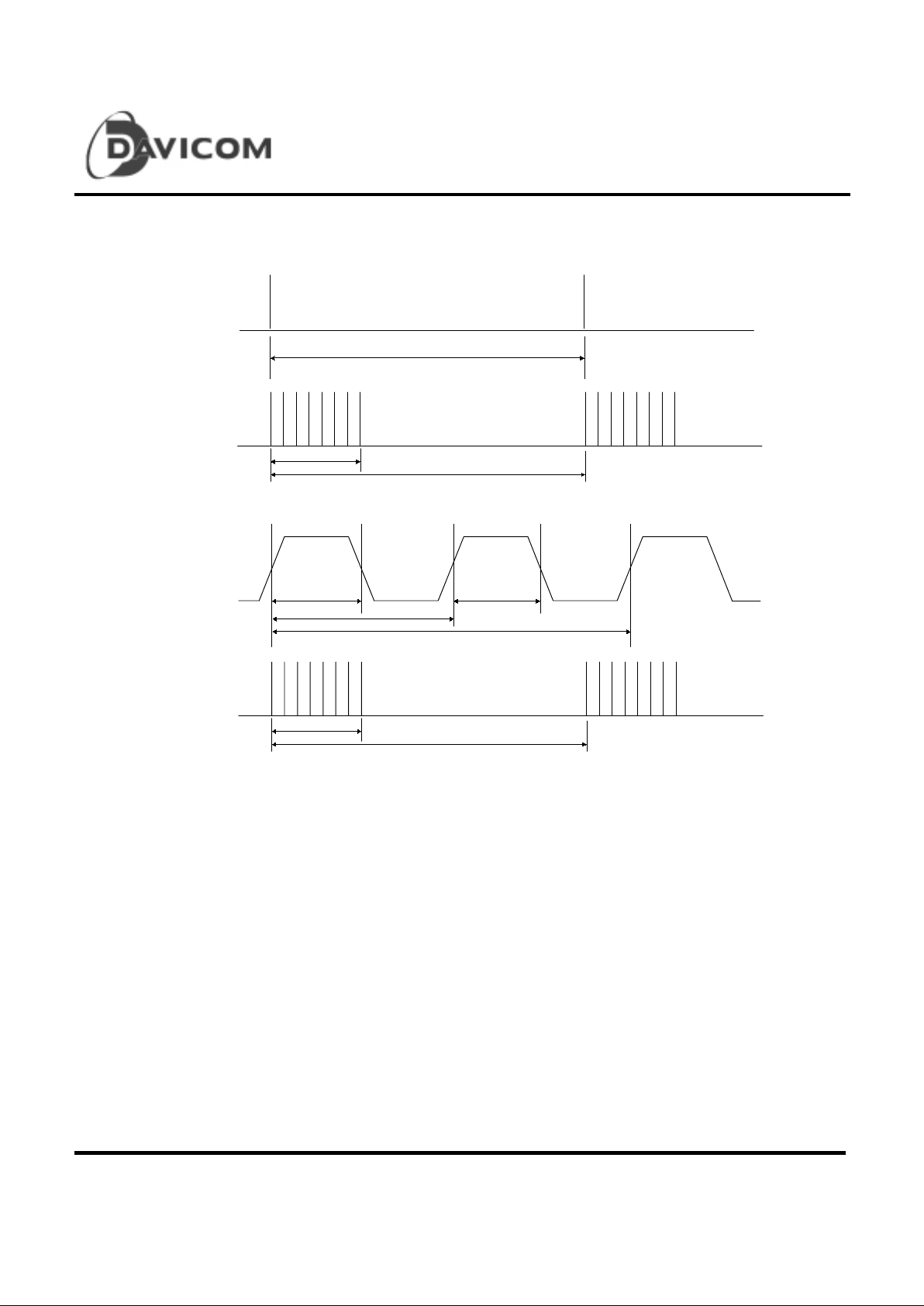
Auto-negotiation and Fast Link Pulse Timing Parameters
Symbol Parame ter Min. Typ. Max. Unit Conditions
t
1
Clock/Data Pulse Width --- 100 --- ns
t
2
Clock Pulse To Data Pulse Period 55.5 62.5 69.5 us DATA = 1
t
3
Clock Pulse To Clock Pulse Period 111 125 139 us
t
4
FLP Burst Width - 2 - ms
t
5
FLP Burst To FLP Burst Period 8 24 ms
- Clock/Data Pulses in a Burst 17 33 pulse
Page 28
DM9131
10/100 Mbps Fast Ethernet Physical Layer Si ngle Chi p Transceiver
28 Final
Version: DM9131-DS-F01
April 7, 2000
Auto-negotiation and Fast Link Pulse Timing Diagram
FLP Bursts
t
3
FLP Burst FLP Burst
t
4
t
5
NLPs
FAST LINK
PULSES
Clock Pulse Data Pulse Clock Pulse
t
1
t
2
t
3
FLP Burst
FLP Burst
t
4
t
5
10TX0+/-
t
1
Page 29
DM9131
10/100 Mbps Fast Ethernet Physical Layer Si ngle Chi p Transceiver
Final 29
Version: DM9131-DS-F01
April 7, 2000
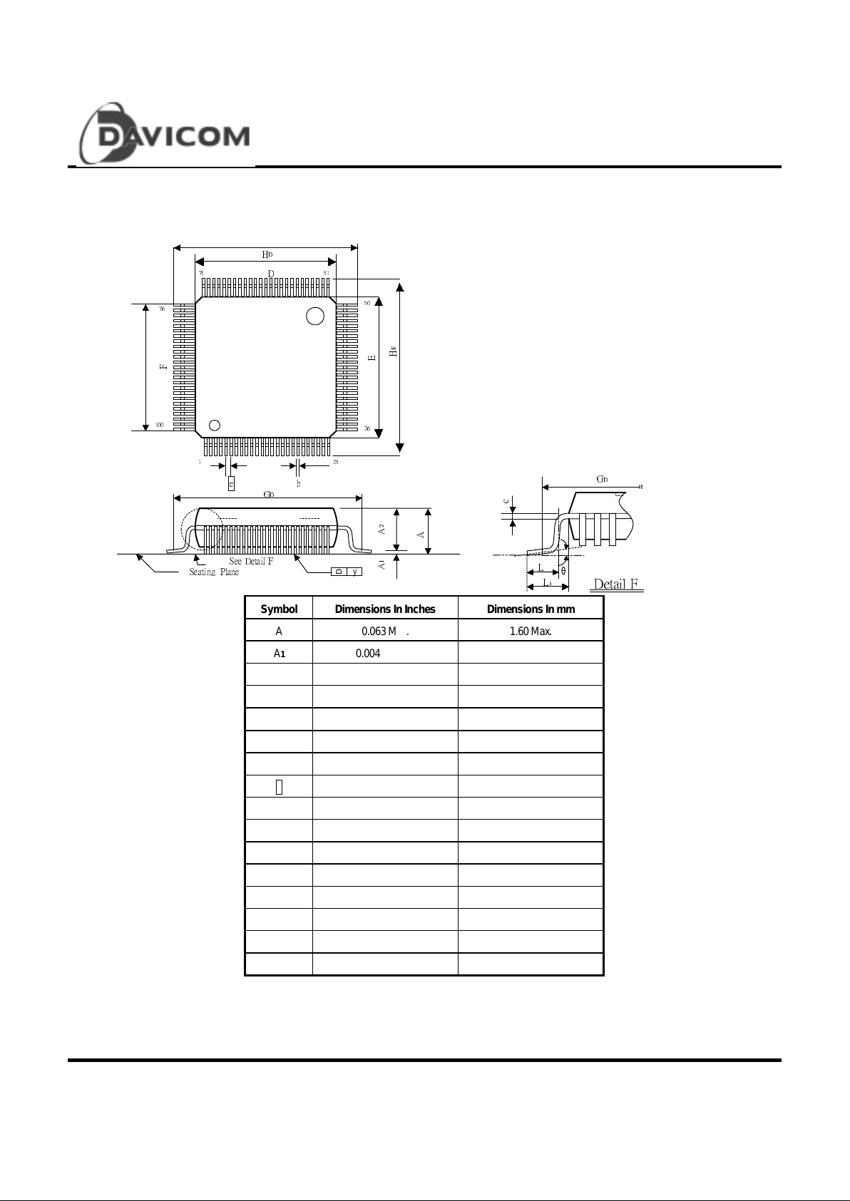
Package Infor mation
LQFP 100L Outline Dime nsions
Unit: Inche s /mm
D
y
Symbol Dimensions In Inches Dimensions In mm
A 0.063 Max. 1.60 Max.
A
1
0.004 ± 0.002 0.1 ± 0.05
A
2
0.055 ± 0.002 1.40 ± 0.05
b0.009
± 0.002
0.22
± 0.05
c0.006
± 0.002
0.15
± 0.05
D 0.551 ± 0.005 14.00 ± 0.13
E 0.551 ± 0.005 14.00 ± 0.13
e
0.020 BSC. 0.50 BSC.
F 0.481 NOM. 12.22 NOM.
G
D
0.606 NOM. 15.40 NOM.
H
D
0.630 ± 0.006 16.00 ± 0.15
H
E
0.630 ± 0.006 16.00 ± 0.15
L 0.024 ± 0.006 0.60 ± 0.15
L
1
0.039 Ref. 1.00 Ref.
y 0.004 Max. 0.1 Max.
θ 0° ~ 12° 0° ~ 12°
Note:
1. Dimension D & E do not include resin fins.
2. Dimension GD is for PC Board surface mount pad pitch design reference only.
3. All dimensions are based on metric system.
Page 30

DM9131
10/100 Mbps Fast Ethernet Physical Layer Si ngle Chi p Transceiver
30 Final
Version: DM9131-DS-F01
April 7, 2000
Ordering Information
Part Num ber Pin Count Package
DM9131 100 LQFP
Disclaimer
The information appearing in this publication is believed to
be accurate. Integrated circuits sold by DAVICOM
Semiconductor are covered by the warranty and patent
indemnification provisions s tipulated in the terms of sale
only. DAVICOM makes no warranty, express, statutory,
implied or by description regarding the information in this
publication or regarding the information in this publication or
regarding the freedom of the described chip(s) from patent
infringement. FURTHER, DAVICOM MAKES NO
WARRANTY OF MERCHANTABILITY OR FITNESS
FOR ANY PURPOSE. DAVICOM deserves the right to halt
production or alter the specifications and prices at any time
without notice. Accordingly, the reader is cautioned to verify
that the data sheets and other information in this publication
are current before placing orders. Products described herein
are intended for use in normal commercial application s.
Applications involving unusual environmental or reliability
requirements, e.g. military equipment or medical life support
equipment, are specifically not recommended without
additional processing by DAVICOM for such applica tion s.
Please note that application circuits illustrated in this
document are for reference purposes only.
DAVICOM’s terms and conditions printed on the order
acknowledgment govern all sales by DAVICOM.
DAVIC OM will not be bound by any terms inconsistent with
these unless DAVICOM agrees otherwise in writing.
Acceptance of the buyer’s orders shall be based on these
terms.
Company Ov erview
DAVICOM Semiconductor, Inc. develops and
manufactures integrated circuits for integration into data
communica tion pro ducts. O ur mission is to design and
produce IC products that re the industry’s best value for
Data, Audio, Video, and Internet/Intranet applications. To
achieve this goal, we have built an organization that is able
to develop chipsets in response to the evolving technology
requirements of our customers while still deliver ing p r oducts
that meet their cost requirements.
Products
We offer only products that satisfy high performa nce
requirements and which are compatible with major
hardware and software standards. Our currently available
and soon to be released products are based on our
proprietary designs and deliver high quality, high
performance chipsets that comply with modem
communication standards and Ethernet networking
standards.
Contact Windows
For additional information about DAVICOM products, contact the sale s department at:
Headquar ter s
Hsin-chu Office:
3F, No. 7-2, Industry E. Rd., IX,
Science-based Park,
Hsin-c hu C ity, Taiw an , R.O.C .
TEL: 886-3-5798797
FAX: 886-3-5798858
Taipei Sales & Marketing Office:
8F, No. 3, Lane 235, Bao-chiao Rd.,
Hsin-tie n, Taip ei, Taiw an , R.O.C .
TEL: 02-29153030
FAX: 02-29157575
Email: [email protected]
Davicom USA
Sunnyvale, California
1135 Kern Ave., Sunnyvale,
CA94086, U.S.A.
TEL: 1-408-7368600
FAX: 1-408-7368688
Email: [email protected]
WARNING
Conditions beyond those listed for the absolute maximum may destroy or damage the products. In addition, conditions for su stained periods at near the limits
of the operating ra nges will stress and may tempo rarily (and perm anently) affect and damage structure, performance and/or function.
 Loading...