

National Semiconductor CLC412 Technical data
N
CLC412
Dual Wideband Video Op Amp
June 1999
CLC412
Dual Wideband Video Op Amp
General Description
The CLC412 combines a high-speed complementary bipolar process
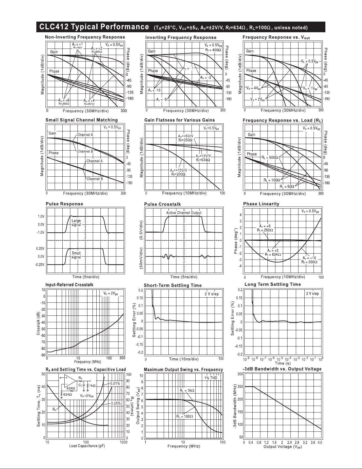
with National's current-feedback topology to produce a very highspeed dual op amp. The CLC412 provides a 250MHz small-signal
bandwidth at a gain of +2V/V and a 1300V/µs slew rate while
consuming only 50mW per amplifier from ±5V supplies.
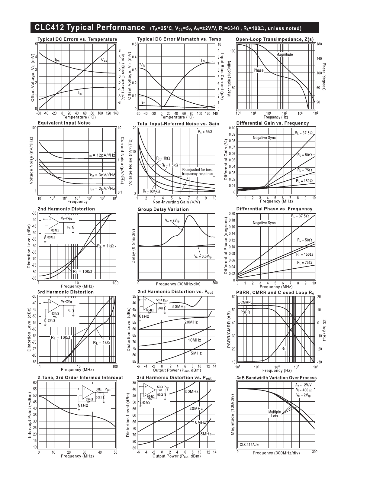
The CLC412 offers exceptional video performance with its 0.02%
and 0.02° differential gain and phase errors for NTSC and PAL video
signals while driving one back terminated 75Ω load. The CLC412
also offers a flat gain response of 0.1dB to 30MHz and very low
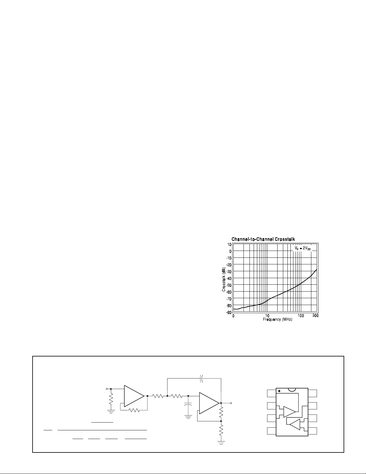
channel-to-channel crosstalk of -76dB at 10MHz. Additionally, each
amplifier can deliver a 70mA continuous output current. This level of
performance makes the CLC412 an ideal dual op amp for highdensity broadcast-quality video systems.
The CLC412's two very well-matched amplifiers support a number of
applications such as differential line drivers and receivers. In
addition, the CLC412 is well suited for Sallen Key active filters in
applications such as anti-aliasing filters for high-speed A/D
converters. Its small 8-pin SOIC package, low power requirement,
low noise and distortion allow the CLC412 to serve portable RF
applications such as IQ-channels.
The CLC412 is available in the following versions.
Features
■ Wide bandwidth: 330MHz (A
250MHz (Av=+2V/V)
■ 0.1dB gain flatness to 30MHz
■ Low power: 5mA/channel
■ Very low diff. gain, phase: 0.02%, 0.02°
■ -76dB channel-to-channel crosstalk
(10MHz)
■ Fast slew rate: 1300V/µs
■ Unity-gain stable
=+1V/V)
v
Applications
■ HDTV, NTSC & PAL video systems
■ Video switching and distribution
■ IQ amplifiers
■ Wideband active filters
■ Cable drivers
■ DC coupled single-to-differential conversions
CLC412AJP -40°C to +85°C 8-pin Plastic DIP
CLC412AJE -40°C to +85°C 8-pin Plastic SOIC
CLC412AIB -40°C to +85°C 8-pin CERDIP
CLC412A8B -55°C to +125°C 8-pin CERDIP,
MIL-STD-883, Level B
CLC412A8L-2A -55°C to +125°C 20-pin LCC,
MIL-STD-883, Level B
CLC412AMC -55°C to +125°C dice,
MIL-STD-883, Level B
DESC SMD number: 5962-94719
Typical Application
Sallen-Key Low-Pass Filter
V
in
V
V
out
=
11
2
in
ss
+++
RC RCKRC RRCC
11 2 2922 1212
K
o
RR CC
1212
1
+
½CLC412
R
in
R
f
−
+
1
R
R
1
2
C
2
C
1
+
½CLC412
-
Pinout
DIP & SOIC
1
1
V
V
non-inv
out
V
inv
-Vcc
2
1
1
+
3
4
+
V
out
R
f
R
g
+V
8
cc
V
out
V
inv
V
non-inv
2
2
2
7
6
5
1999 National Semiconductor Corporation http://www.national.com
Printed in the U.S.A.
CLC412 Electrical Characteristics (A
= +2; R
V
= 634
f
ΩΩ
Ω; V
ΩΩ
= ±5V; R
CC
= 100
L
ΩΩ
Ω)
ΩΩ
PARAMETERS CONDITIONS TYP MIN/MAX RATINGS UNITS SYMBOL
Ambient Temperature CLC412 AJ +25°C -40°C +25°C +85°C
FREQUENCY DOMAIN RESPONSE
-3dB bandwidth V
gain flatness V
peaking DC to 30MHz 0.1 0.1 0.1 0.2 dB GFP
V
< 0.5V
out
< 4.0V
out
< 0.5V
out
pp
pp
pp
25 0 15 0 175 13 5 M Hz SSBW
10 5 80 80 65 MHz LSBW
rolloff DC to 30MHz 0.1 0.4 0.3 0.3 dB GFR
linear phase deviation DC to 75MHz 0.5 1.3 1.0 1.0 deg LPD
differential gain 4.43MHz, R
differential phase 4.43MHz, R
=150Ω 0.02 0.04 0.04 0.08 % DG
L
=150Ω 0.02 0.04 0.04 0.08 deg DP
L
TIME DOMAIN RESPONSE
rise and fall time 0.5V step 1.4 2.3 2.0 2.6 ns TRS
4V step 3.2 4.4 4.4 4.8 ns TRL
settling time to 0.05% 2V step 12 18 18 20 ns TSS
overshoot 0.5V step 8 15 15 15 % OS
slew rate 2V step 13 00 10 00 1000 800 V/µsSR
DISTORTION AND NOISE RESPONSE
nd
harmonic distortion 2Vpp, 20MHz - 4 6 - 42 - 42 - 38 dBc HD2
2
rd
harmonic distortion 2Vpp, 20MHz - 5 0 - 46 - 46 - 42 dBc HD 3
3
rd
order intermodulation intercept 10MHz 43 dBm
3
1Hz
IMD
equivalent noise input
non-inverting voltage >1MHz 3.0 3.4 3.4 3.8 nV/√Hz VN
inverting current >1MHz 12.0 13.9 13.9 15.5 pA/√Hz NICN
non-inverting current >1MHz 2.0 2.6 2.6 3.0 pA/√Hz ICN
noise floor >1MHz - 1 57 - 156 - 156 - 1 55 dBm
1Hz
SNF
crosstalk input-referred 10MHz - 76 - 70 - 70 - 70 dB XTLKA
STATIC DC PERFORMANCE
*input offset voltage ± 2 ± 1 0 ± 6 ± 12 mV VIO
average drift ± 30 ± 60
*input bias current non-inverting ±5 ± 28 ± 12 ± 12 µAIBN
average drift ± 30 ± 18 7
*input bias current inverting ± 3 ± 3 4 ± 1 5 ± 20 mA IBI
average drift ± 20 ± 12 5
____
____
____
±60 µV/°C DVIO
± 90 nA/°C DIBN
± 80 nA/°C DIBI
power supply rejection ratio DC 50 46 46 44 dB PSRR
common mode rejection ratio D C 50 45 4 5 4 3 d B CMRR
*supply current R
= ∞ 10.2 13.6 12.8 12.8 mA ICC
L
MISCELLANEOUS PERFORMANCE
input resistance non-inverting 1000 300 500 500 kΩ RIN
input capacitance non-inverting 1.0 2.0 2.0 2.0 pF CIN
output resistance closed loop 0.04 0.6 0.3 0.2 Ω ROUT
output voltage range R
= ∞
L
=100Ω
R
L
=100Ω (0° to 70°C)
R
L
+ 3.8,-3.3 +3.6,-2.9 + 3.7,-3.0 + 3.7,-3.0
+ 3.1,-2.9 +2.0,-2.5
± 2.7 ± 2.7 V VOL
+ 2.5,-2.6
VVO
V VOLC
input voltage range common mode ± 2.2 ± 1.4 ± 2.0 ± 2.0 V CMIR
output current 70 25 45 45 mA IO
Min/max ratings are based on product characterization and simulation. Individual parameters are tested as noted. Outgoing quality levels
are determined from tested parameters.
Absolute Maximum Ratings Miscellaneous Ratings
V
cc
I
short circuit protected to ground, however maximum reliabiliy
out
is obtained if I
common-mode input voltage ± V
maximum junction temperature +150°C
operating temperature range: AJ -40°C to +85°C
storage temperature range -65°C to +150°C
lead temperature (soldering 10 sec) +300°C
ESD (100V machine test) 1000V
does not exceed... 125mA
out
Reliability Information
Transistor count 68
http://www.national.com 2
±7V
Recommended gain range ±1 to ±10V/V
Notes:
cc
* AJ : 100% tested at +25°C.
Package Thermal Resistance
Package
AJP 70°C/W 125°C/W
AJE 65°C/W 145°C/W
A8B 40°C/W 130°C/W
θθ
θ
θθ
JC
θθ
θ
θθ
JA
3 http://www.national.com
http://www.national.com 4
 Loading...