

CLC021
SMPTE 259M Digital Video Serializer with EDH
Generation and Insertion
CLC021 SMPTE 259M Digital Video Serializer with EDH Generation and Insertion
July 2003
General Description
The CLC021 SMPTE 259M Digital Video Serializer with EDH
Generation and Insertion is a monolithic integrated circuit
that encodes, serializes and transmits bit-parallel digital data
conforming to SMPTE 125M and 267M component video
and SMPTE 244M composite video standards. The CLC021
can also serialize other 8- or 10-bit parallel data. The
CLC021 operates at data rates from below 100 Mbps to over
400 Mbps. The serial data clock frequency is internally generated and requires no external frequency setting, trimming
or filtering components*.
Functions performed by the CLC021 include: parallel-toserial data conversion, ITU-R BT.601-4 input data clipping,
data encoding using the SMPTE polynomial (X
format conversion from NRZ to NRZI, parallel data clock
frequency multiplication and encoding with the serial data,
and differential, serial output data driving. The CLC021 has
circuitry for automatic EDH character and flag generation
and insertion per SMPTE RP-165. The CLC021 has an
exclusive built-in self-test (BIST) and video test pattern generator (TPG) with 16 component video test patterns: reference black, PLL and EQ pathologicals and modified colour
bars in 4:3 and 16:9 raster formats for NTSC and PAL
formats*.
The CLC021 has inputs for enabling sync detection, nonSMPTE mode operation, enabling the EDH function, NRZ/
NRZI mode control and an external reset control. Outputs
are provided for H, V and F bits, new TRS sync character
position indication, ancilliary data header detection, NTSC/
PAL raster indication and PLL lock detect. Separate power
pins for the output driver, VCO and the serializer improve
power supply rejection, output jitter and noise performance.
The CLC021AVGZ-5.0V is powered by a single +5V supply.
The CLC021AVGZ-3.3V is powered by a single +3.3V supply. Power dissipation is typically 235 mW including two 75Ω
back-matched output loads. The device is packaged in a
JEDEC metric 44-lead PQFP.
9+X4
+1), data
Features
n SMPTE 259M serial digital video standard compliant
n Supports all NTSC and PAL standard component and
composite serial video data rates
n No external serial data rate setting or VCO filtering
components required
n Fast VCO lock time:<75 µs at 270 Mbps
n Built-in self-test (BIST) and video test pattern generator
(TPG) with 16 internal patterns
n Automatic EDH character and flag generation and
insertion per SMPTE RP 165
n Non-SMPTE mode operation as parallel-to-serial
converter
n NRZ-to-NRZI conversion control
n HCMOS/LSTTL-compatible data and control inputs and
outputs for CLC021AVGZ-5.0, LVCMOS for
CLC021AVGZ-3.3
n 75Ω ECL-compatible, differential, serial cable-driver
outputs
n Single power supply operation: 5V (CLC021AVGZ-5.0)
or 3.3V (CLC021AVGZ-3.3) in TTL or ECL systems
n Low power: typically 235 mW
n JEDEC 44-lead metric PQFP package
n Commercial temperature range 0˚C to +70˚C
*
Patents applications made or pending.
*
*
Applications
n SMPTE 259M parallel-to-serial digital video interfaces
for:
— Video cameras
— VTRs
— Telecines
— Video test pattern generators and digital video test
equipment
— Video signal generators
n Non-SMPTE video applications
n Other high data rate parallel/serial video and data
applications
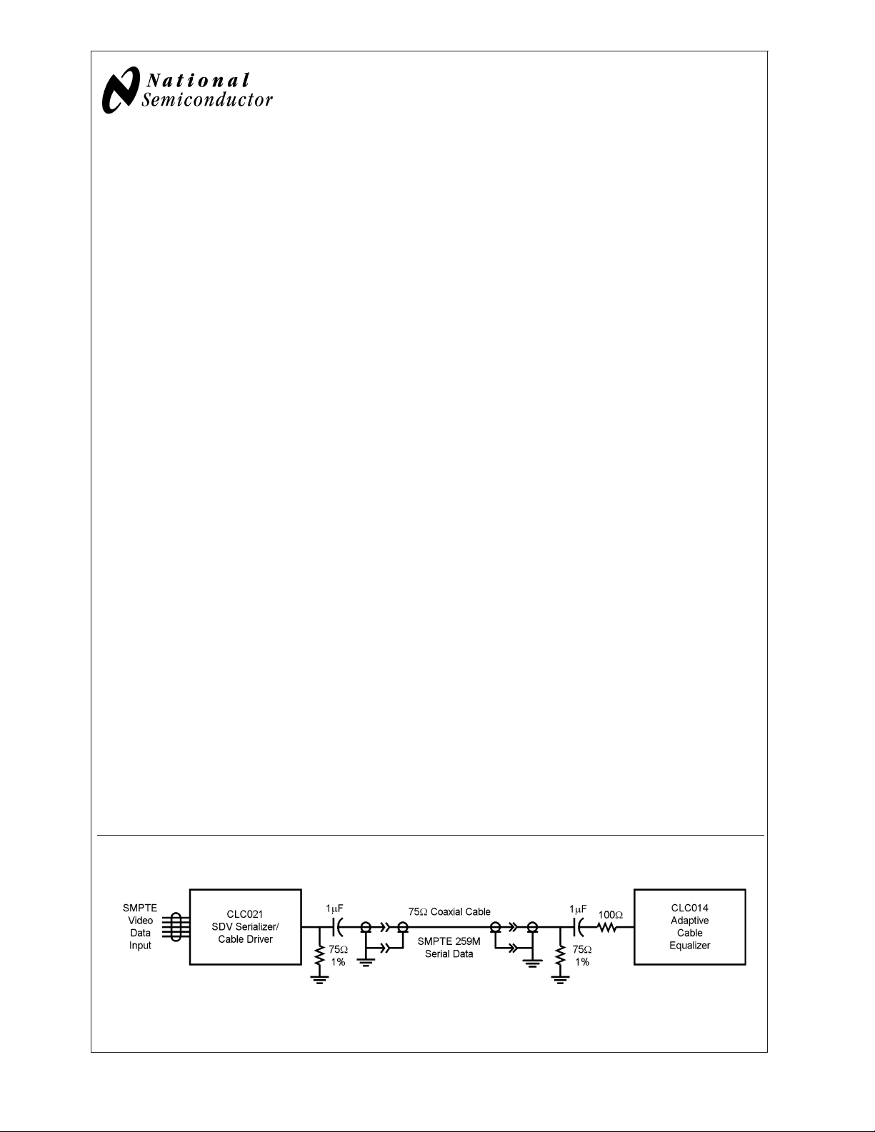
Typical Application
10136812
© 2003 National Semiconductor Corporation DS101368 www.national.com
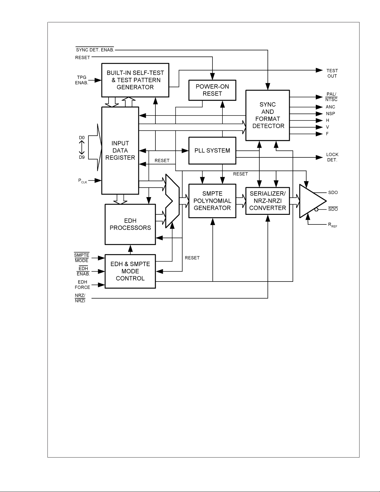
Block Diagram
CLC021
www.national.com 2
10136801
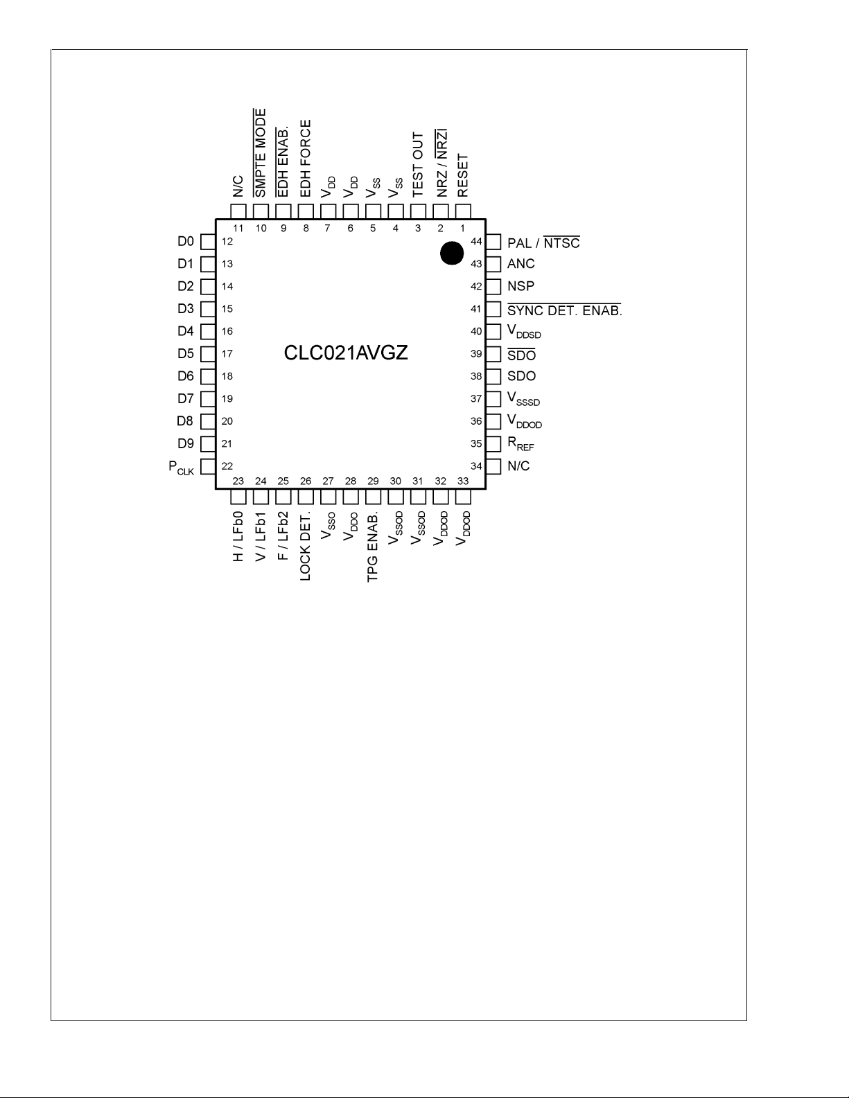
Connection Diagram
CLC021
44-Pin Metric PQFP
Order Number CLC021AVGZ-5.0 or CLC021AVGZ-3.3
See NS Package Number VGZ44A
10136802
www.national.com3
Absolute Maximum Ratings (Note 1) It
is anticipated that this device will not be offered in a
CLC021
military qualified version. If Military/Aerospace specified devices are required, please contact the National
Semiconductor Sales Office / Distributors for availability and specifications.
Supply Voltage (V
CLC021AVGZ-5.0V 6.0V
CLC021AVGZ-3.3V 4.0V
CMOS/TTL Input Voltage (V
CLC021AVGZ-5.0V −0.5V to V
CLC021AVGZ-3.3V -0.3V to V
CMOS/TTL Output Voltage (V
CLC021AVGZ-5.0V −0.5V to V
CLC021AVGZ-3.3V -0.3V to V
CMOS/TTL Input Current (single input):
V
I=VSS
V
I=VDD
−0.5V: −5 mA
+0.5V: +5 mA
Input Current, Other Inputs:
CMOS/TTL Output Source/Sink Current:
SDO Output Source Current: 22 mA
Package Thermal Resistance
θ
44-lead Metric PQFP:
JA
@
(
0 LFM airflow) 60˚C/W
@
(
500 LFM airflow) 43˚C/W
DD−VSS
):
):
I
):
O
+0.5V
DD
+0.3V
DD
+0.5V
DD
+0.3V
DD
±
±
16 mA
1mA
θ
44-lead Metric PQFP: 17˚C/W
JC
Storage Temp. Range: −65˚C to +150˚C
Junction Temperature: +150˚C
Lead Temperature (Soldering 4
+260˚C
Sec):
ESD Rating (HBM): 2 kV
ESD Rating (MM): 150V
Transistor Count: 33,400
Recommended Operating Conditions
Supply Voltage (VDD−VSS):
CLC021AVGZ-5.0 5.0V
CLC021AVGZ-3.3 3.3V
CMOS/TTL Input Voltage: V
Maximum DC Bias on SDO pins:
CLC021AVGZ-5.0 3.0V
CLC021AVGZ-3.3 1.3V
P
Frequency Range 10 to 40MHz
CLK
P
Duty Cycle 45 to 55%
CLK
D
N
and P
Rise/Fall Time 1.0 to 3.0 ns
CLK
Operating Free Air Temperature
):
(T
A
±
10%
±
10%
to V
SS
±
10%
±
10%
0˚C to +70˚C
DD
DC Electrical Characteristics—CLC021AVGZ-5.0
Over Supply Voltage and Operating Temperature ranges, unless otherwise specified (Notes 2, 3).
Symbol Parameter Conditions Reference Min Typ Max Units
V
IH
V
IL
I
IH
I
IL
V
OH
V
OL
V
SDO
Input Voltage High Level
Input Voltage Low Level V
Input Current High Level VIH=V
Input Current Low Level VIL=V
CMOS Output Voltage
DD
SS
IOH= −10 mA
High Level
CMOS Output Voltage
IOL= +10 mA
All CMOS Inputs
All CMOS
Outputs
Low Level
Serial Driver Output
Voltage
RL=75Ω 1%,
= 1.69 kΩ 1%,
R
REF
SDO, SDO 700 800 900 mV
2.0 V
SS
+40 +60 µA
-1 -20 µA
2.4 4.7 V
0.0 0.3 V
SS
DD
0.8 V
DD
+ 0.5V V
Figure 2
I
DD
Power Supply Current,
Total
RL=75Ω 1%,
= 1.69 kΩ 1%,
R
REF
= 27 MHz, NTSC
P
CLK
47 60 mA
Colour Bar Pattern,
Figure 2
DC Electrical Characteristics—CLC021AVGZ-3.3
Over Supply Voltage and Operating Temperature ranges, unless otherwise specified (Notes 2, 3).
Symbol Parameter Conditions Reference Min Typ Max Units
V
IH
V
IL
I
IH
I
IL
Input Voltage High Level
Input Voltage Low Level V
Input Current High Level VIH=V
Input Current Low Level VIL=V
DD
SS
All CMOS Inputs
2.0 V
SS
+22 +60 µA
-1 -20 µA
DD
0.6 V
V
V
P-P
V
www.national.com 4
DC Electrical Characteristics—CLC021AVGZ-3.3 (Continued)
Over Supply Voltage and Operating Temperature ranges, unless otherwise specified (Notes 2, 3).
Symbol Parameter Conditions Reference Min Typ Max Units
V
OH
V
OL
V
SDO
CMOS Output Voltage
High Level
CMOS Output Voltage
Low Level
Serial Driver Output
Voltage
IOH=−8mA
IOL=+8mA
RL=75Ω 1%,
= 1.69 kΩ 1%,
R
REF
All CMOS
Outputs
2.4 3.0 V
0.0 0.3 V
DD
+ 0.5V V
SS
SDO, SDO 720 800 880 mV
Figure 2
I
DD
Power Supply Current,
Total
RL=75Ω 1%,
= 1.69 kΩ 1%,
R
REF
= 27 MHz, NTSC
P
CLK
33 55 mA
Colour Bar Pattern,
Figure 2
AC Electrical Characteristics—CLC021AVGZ-5.0
Over Supply Voltage and Operating Temperature ranges, unless otherwise specified (Note 3).
Symbol Parameter Conditions Reference Min Typ Max Units
BR
F
P
t
r,tf
t
j
t
jit
tr,t
t
LOCK
t
SU
t
HLD
L
GEN
R
GEN
SDO
CLK
f
Serial Data Rate (Note 5) SDO, SDO 100 400 Mbps
Reference Clock
Input Frequency
Reference Clock Duty
Cycle
Rise Time, Fall Time DN,P
P
CLK
P
CLK
CLK
Serial Output Jitter 270 Mbps,Figure 2, (Note 6)
Serial Output Jitter (Notes 4, 5) 100 200 ps
Rise Time, Fall Time 20%–80%, (Notes 4, 5) 500 800 1500 ps
SDO, SDO
10 40 MHz
45 50 55 %
1.0 1.5 3.0 ns
220 ps
Output Overshoot (Note 4) 1 %
Lock Time (Notes 5, 7) 75 µs
Setup Time Figure 3 (Note 4) DNto P
Hold Time Figure 3 (Note 4) DNfrom P
Output Inductance (Note 4)
Output Resistance (Note 4) 25k Ω
CLK
CLK
SDO, SDO
32 ns
32 ns
6nH
CLC021
V
P-P
P-P
P-P
AC Electrical Characteristics—CLC021AVGZ-3.3
Over Supply Voltage and Operating Temperature ranges, unless otherwise specified (Note 3).
Symbol Parameter Conditions Reference Min Typ Max Units
BR
F
P
t
r,tf
t
j
t
jit
tr,t
t
LOCK
t
SU
t
HLD
SDO
CLK
f
Serial Data Rate (Note 5) SDO, SDO 100 400 Mbps
Reference Clock
Input Frequency
Reference Clock Duty
Cycle
Rise Time, Fall Time DN,P
P
CLK
P
CLK
CLK
Serial Output Jitter 270 Mbps,Figure 2, (Note 6)
Serial Output Jitter (Notes 4, 5) 100 200 ps
Rise Time, Fall Time 20%–80%, (Notes 4, 5) 500 800 1500 ps
SDO, SDO
10 40 MHz
45 50 55 %
1.0 1.5 3.0 ns
220 ps
Output Overshoot (Note 4) 1 %
Lock Time (Notes 5, 7) 75 µs
Setup Time Figure 3 (Note 4) DNto P
CLK
Hold Time Figure 3 (Note 4) DNfrom P
CLK
42 ns
42 ns
www.national.com5
P-P
P-P
AC Electrical Characteristics—CLC021AVGZ-3.3 (Continued)
Over Supply Voltage and Operating Temperature ranges, unless otherwise specified (Note 3).
CLC021
Symbol Parameter Conditions Reference Min Typ Max Units
L
GEN
R
GEN
Note 1: “Absolute Maximum Ratings” are those parameter values beyond which the life and operation of the device cannot be guaranteed. The stating herein of
these maximums shall not be construed to imply that the device can or should be operated at or beyond these values. The table of “Electrical Characteristics”
specifies acceptable device operating conditions.
Note 2: Current flow into device pins is defined as positive. Current flow out of device pins is defined as negative. All voltages are stated referenced to V
Note 3: Typical values are stated for V
Note 4: Specification is guaranteed by design.
Note 5: R
Note 6: CLC021 mounted in the SD021EVK board, configured in BIST mode (NTSC colour bars) with P
reference. Timing jitter measured with Tektronix VM700T using jitter measurement FFT mode, frame rate, 1 kHz filter bandwidth, Hanning window.
Note 7: Measured from rising-edge of first P
Output Inductance (Note 4)
Output Resistance (Note 4) 25k Ω
= +5.0V (CLC021AVGZ-5.0) or +3.3V (CLC021AVGZ-3.3) and TA= +25˚C.
DD
=75Ω, AC-coupled@270 M
L
bps,RREF
= 1.69 kΩ 1%, See Test Loads and Figure 2.
cycle until Lock Detect output goes high (true).
CLK
SDO, SDO
CLK
= 27 MHz derived from Tektronix TG2000 black-burst
6nH
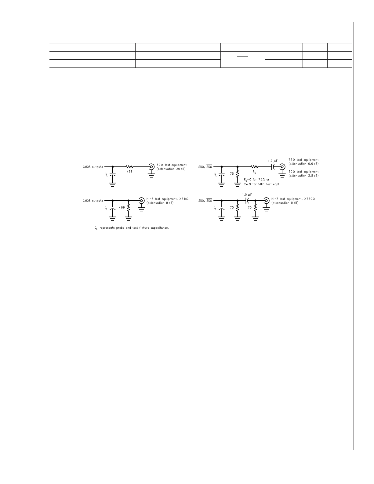
Test Loads
=0V.
SS
FIGURE 1. Test Loads
10136803
www.national.com 6
 Loading...