

查询74C2525供应商
CGS74C2525#CGS74CT2525
CGS74C2526
1-to-8 Minimum Skew Clock Driver
CGS74CT2526
#
September 1995
CGS74C2525
1-to-8 Minimum Skew Clock Driver
#
CGS74CT2525
The CGS ’C/CT2525 is a minimum skew clock driver with
one input driving eight outputs specifically designed for signal generation and clock distribution applications. The ’2525
is designed to distribute a single clock to eight separate
receivers with low skew across all outputs during both the
t
and t
PLH
but contains a multiplexed clock input to allow for systems
with dual clock speeds or systems where a separate test
clock has been implemented.
transitions. The ’2526 is similar to the ’2525
PHL
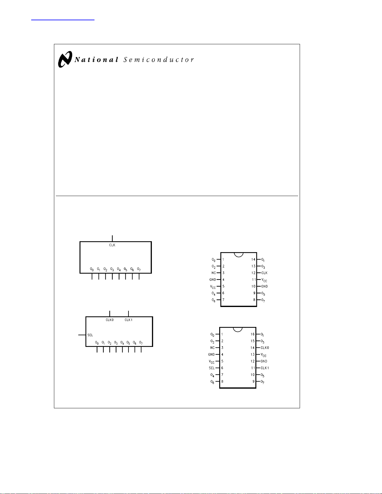
Logic Symbols
’2525
TL/F/10684– 1
Features
Y
These CGS devices implement National’s FACT
family
Y
Ideal for signal generation and clock distribution
Y
Guaranteed pin to pin and part to part skew
Y
Multiplexed clock input (’2526)
Y
Guaranteed 2 kV minimum ESD protection
Y
Symmetric output current drive of 24 mA for IOL/I
Y
’CT has TTL-compatible inputs
Y
These products are identical to 74AC/ACT2525 and
2526
Y
Available as Mil/Aero versions
54AC/ACT2525
54AC/ACT2526
TM
Connection Diagrams
Pin Assignment
for DIP and SOIC
’2525
OH
#
CGS74C2526
#
CGS74CT2526
’2526
TL/F/10684– 2
TRI-STATEÉis a registered trademark of National Semiconductor Corporation.
TM
FACT
is a trademark of National Semiconductor Corporation.
C
1996 National Semiconductor Corporation RRD-B30M106/Printed in U. S. A.
TL/F/10684
TL/F/10684– 3
’2526
TL/F/10684– 4
http://www.national.com
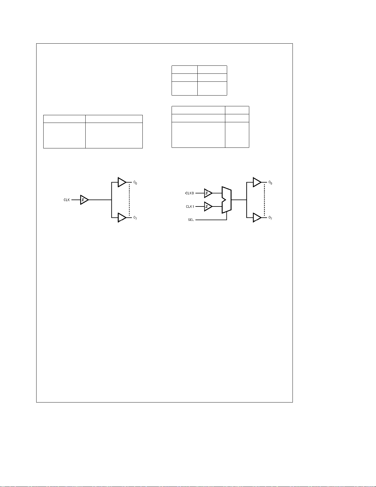
Functional Description
On the multiplexed clock device, the SEL pin is used to
determine which CLKn input will have an active effect on
the outputs of the circuit. When SEL
selected and when SEL
e
The non-selected CLKn input will not have any effect on the
logical output level of the circuit. The output pins act as a
single entity and will follow the state of the CLK or
CLK1/CLK0 pins when either the multiplexed (’2526) or the
straight (’2525) clock distribution chip is selected.
Pin Description
Pin Names Description
CLK Clock Input (’2525)
CLK0, CLK1 Clock Inputs (’2526)
O
0–O7
SEL Clock Select (’2526)
Outputs
e
1, the CLK1 input is
0, the CLK0 input is selected.
Truth Tables
’2525
Inputs Outputs
CLK O0–O
LL
HH
Inputs Outputs
CLK0 CLK1 SEL O0–O
LXL L
HXL H
XLH L
XHH H
e
L
Low Voltage Level
e
H
High Voltage Level
e
X
Immaterial
7
’2526
7
’2525
TL/F/10684– 7
’2526
TL/F/10684– 8
http://www.national.com 2

Absolute Maximum Ratings (Note 1)
If Military/Aerospace specified devices are required,
please contact the National Semiconductor Sales
Office/Distributors for availability and specifications.
Supply Voltage (V
DC Input Diode Current (IIK)
eb
V
0.5V
I
e
V
V
I
CC
)
CC
a
0.5V
DC Input Voltage (VI)
DC Output Diode Current (IOK)
e
V
0.5V
O
e
V
a
V
CC
0.5V
O
DC Output Voltage (VO)
DC Output Source
or Sink Current (I
)
O
DC VCCor Ground Current
per Output Pin (I
Storage Temperature (T
Junction Temperature (i
Plastic (N) 14-Lead 102
CC
or I
GND
STG
JA
)
)
)
Plastic (M) 14-Lead 128
Plastic (N) 16-Lead 97
Plastic (M) 16-Lead 124
b
b
0.5V to (V
b
0.5V to (V
b
65§Ctoa150§C
0.5V toa7.0V
b
20 mA
a
0.2 mA
a
0.5V)
CC
b
20 mA
a
20 mA
a
0.5V)
CC
g
50 mA
g
50 MA
C/W
§
C/W
§
C/W
§
C/W
§
Recommended Operating
Conditions
Supply Voltage (VCC)
‘C’ 2.0V to 6.0V
‘CT’ 4.5V to 5.5V
Input Voltage (V
Output Voltage (VO) 0VtoV
Operating Temperature (TA)
CGS74C/CT
54AC/ACT
Input Rise and Fall Times Devices
(30% to 70% of V
V
CC
Input Rise and Fall Times Devices
(0.8V to 2.0V) 9.6 ns max
Note 1: Absolute maximum ratings are those values beyond which damage
to the device may occur. The databook specifications should be met, without
exception, to ensure that the system design is reliable over its power supply,
temperature, and output/input loading variables. National does not recommend operation of CGS circuits outside databook specifications.
) 0VtoV
I
)
e
3.3V 10.5 ns max
CC
4.5V 14.4 ns max
5.5V 17.6 ns max
DC Electrical Characteristics for CGS74C and 54AC Family Devices
Over recommended operating conditions unless specified otherwise.
CGS74C 54AC CGS74C
Symbol Parameter
V
IH
V
IL
V
OH
Minimum High Level 3.0 1.5 2.1 2.1 2.1 V
Input Voltage 4.5 2.25 3.15 3.15 3.15 V or V
Maximum Low Level 3.0 1.5 0.9 0.9 0.9 V
Input Voltage 4.5 2.25 1.35 1.35 1.35 V or V
Minimum High Level 3.0 2.99 2.9 2.9 2.9 I
Output Voltage 4.5 4.49 4.4 4.4 4.4 V
(Note 2) 5.5 5.49 5.4 5.4 5.4
V
OL
Maximum Low Level 3.0 0.002 0.1 0.1 0.1 I
Output Voltage 4.5 0.001 0.1 0.1 0.1 V
(Note 2) 5.5 0.001 0.1 0.1 0.1
V
(V)
CC
ea
T
25§C
A
b
e
T
A
55§Ctoa125§Cb40§Ctoa85§C
Typ Guaranteed Limits
5.5 2.75 3.85 3.85 3.85
5.5 2.75 1.65 1.65 1.65
3.0 2.56 2.4 2.46
4.5 3.86 3.7 3.76 V I
5.5 4.86 4.7 4.76
3.0 0.36 0.40 0.44 12 mA
4.5 0.36 0.50 0.44 V
5.5 0.36 0.50 0.44 24 mA
e
T
A
Units Conditions
b
40§Ctoa85§C
b
55§Ctoa125§C
e
OUT
b
CC
e
OUT
b
CC
eb
OUT
e
V
VILor V
IN
b
b
OH
b
e
50 mA
OUT
e
V
VILor V
IN
I
OL
0.1V
0.1V
0.1V
0.1V
50 mA
12 mA
24 mA
24 mA
24 mA
CC
CC
IH
IH
http://www.national.com3
 Loading...