

NAD L-75 Service manual

SERVICE MANUAL
L75
A/V RECEIVER
NAD ELECTRONICS INTERNATIONAL
TORONTO
© NAD 2001

SERVICE MANUAL
L75
A/V RECEIVER
L75
A/V RECEIVER

1-3
SECTION 1
SUMMARY
CONTENTS
PRODUCT SAFETY SERVICING GUIDELINES.......................................................................................... 1-4
SERVICING PRECAUTIONS ....................................................................................................................... 1-5
* General Servicing Precautions
* Insulation checking prodedure
* Electrostatically Sensitive Devices
SPECIFICATIONS ......................................................................................................................................... 1-6
LOCATION OF CUSTOMER CONTROLS ......................................................................................... 1-7 ~ 1-8
EXPLODED VIEW ............................................................................................................................. 1-9 ~ 1-10

1-4
PRODUCT SAFETY SERVICING GUIDELINES
CAUTION : DO NOT ATTEMPT TO MODIFY THIS PRODUCT IN
ANY WAY. NEVER PERFORM CUSTOMIZED INSTALLATIONS
WITHOUT MANUFACTURER’S APPROVAL. UNAUTHORIZED
MODIFICATIONS WILL NOT ONLY VOID THE WARRANTY, BUT
MAY LEAD TO YOUR BEING LIABLE FOR ANY RESULTING
PROPERTY DAMAGE OR USER INJURY.
SERVICE WORK SHOULD BE PERFORMED ONLY AFTER YOU
ARE THOROUGHLY FAMILIAR WITH ALL OF THE FOLLOWING
SAFETY CHECKS AND SERVICING GUIDELINES. TO DO
OTHERWISE, INCREASES THE RISK OF POTENTIAL HAZARDS
AND INJURY TO THE USER.
WHILE SERVICING, USE AN ISOLATION TRANSFORMER FOR
PROTECTION FROM AC LINE SHOCK.
SAFETY CHECKS
AFTER THE ORIGINAL SERVICE PROBLEM HAS BEEN
CORRECTED. A CHECK SHOULD BE MADE OF THE
FOLLOWING.
SUBJECT : FIRE & SHOCK HAZARD
1. BE SURE THAT ALL COMPONENTS ARE POSITIONED IN
SUCH A WAY AS TO AVOID POSSIBILITY OF ADJACENT
COMPONENT SHORTS. THIS IS ESPECIALLY IMPORTANT
ON THOSE MODULES WHICH ARE TRANSPORTED TO AND
FROM THE REPAIR SHOP.
2. NEVER RELEASE A REPAIR UNLESS ALL PROTECTIVE
DEVICES SUCH AS INSULATORS, BARRIERS, COVERS,
SHIELDS, STRAIN RELIEFS, POWER SUPPLY CORDS, AND
OTHER HARDWARE HAVE BEEN REINSTALLED PER
ORIGINAL DESIGN. BE SURE THAT THE SAFETY PURPOSE
OF THE POLARIZED LINE PLUG HAS NOT BEEN DEFEATED.
3. SOLDERING MUST BE INSPECTED TO DISCOVER POSSIBLE
COLD SOLDER JOINTS, SOLDER SPLASHES OR SHARP
SOLDER POINTS. BE CERTAIN TO REMOVE ALL LOOSE
FOREIGN PARTICLES.
4. CHECK FOR PHYSICAL EVIDENCE OF DAMAGE OR
DETERIORATION TO PARTS AND COMPONENTS. FOR
FRAYED LEADS, DAMAGED INSULATION (INCLUDING AC
CORD). AND REPLACE IF NECESSARY FOLLOW ORIGINAL
LAYOUT, LEAD LENGTH AND DRESS.
5. NO LEAD OR COMPONENT SHOULD TOUCH A RECEIVING
TUBE OR A RESISTOR RATED AT 1 WATT OR MORE. LEAD
TENSION AROUND PROTRUDING METAL SURFACES MUST
BE AVOIDED.
6. ALL CRITICAL COMPONENTS SUCH AS FUSES,
FLAMEPROOF RESISTORS, CAPACITORS, ETC. MUST BE
REPLACED WITH EXACT FACTORY TYPES, DO NOT USE
REPLACEMENT COMPONENTS OTHER THAN THOSE
SPECIFIED OR MAKE UNRECOMMENDED CIRCUIT
MODIFICATIONS.
7. AFTER RE-ASSEMBLY OF THE SET ALWAYS PERFORM AN
AC LEAKAGE TEST ON ALL EXPOSED METALLIC PARTS OF
THE CABINET, (THE CHANNEL SELECTOR KNOB, ANTENNA
TERMINALS. HANDLE AND SCREWS) TO BE SURE THE SET
IS SAFET TO OPERATE WITHOUT DANGER OF ELECTRICAL
SHOCK. DO NOT USE A LINE ISOLATION TRANSFORMER
DURING THIS TEST USE AN AC VOLTMETER, HAVING 5000
OHMS PER VOLT OR MORE SENSITIVITY, IN THE
FOLLOWING MANNER; CONNECT A 1500 OHM 10 WATT
RESISTOR, PARALLELED BY A .15 MFD, 150V AC TYPE
CAPACITOR BETWEEN A KNOWN GOOD EARTH GROUND
(WATER PIPE, CONDUIT, ETC.) AND THE EXPOSED
METALLIC PARTS, ONE AT A TIME.
MEASURE THE AC VOLTAGE ACROSS THE COMBINATION
OF 1500 OHM RESISTOR AND .15 MFD CAPACITOR.
REVERSE THE AC PLUG AND REPEAT AC VOLTAGE
MEASUREMENTS FOR EACH EXPOSED METALLIC PART.
VOLTAGE MEASURE MUST NOT EXCEED 75 VOLTS R.M.S.
THIS CORRESPONDS TO 0.5 MILLIAMP AC ANY VALUE
EXCEEDING THIS LIMIT CONSTITUTES A POTENTIAL
SHOCK HAZARD AND MUST BE CORRECTED IMMEDIATELY.
SUBJECT : GRAPHIC SYMBOLS
SUBJECT : TIPS ON PROPER INSTALLATION
1. NEVER INSTALL ANY PRODUCT IN A CLOSED-IN RECESS,
CUBBYHOLE OR CLOSELY FITTING SHELF SPACE. OVER
OR CLOSE TO HEAT DUCT, OR IN THE PATH OF HEATED
AIR FLOW.
2. AVOID CONDITIONS OF HIGH HUMIDITY SUCH AS:
OUTDOOR PATIO INSTALLATIONS WHERE DEW IS A
FACTOR, NEAR STEAM RADIATORS WHERE STEAM
LEAKAGE IS A FACTOR, ETC.
3. AVOID PLACEMENT WHERE DRAPERIES MAY OBSTRUCT
REAR VENTING. THE CUSTOMER SHOULD ALSO AVOID THE
USE OF DECORATIVE SCARVES OR OTHER COVERINGS
WHICH MIGHT OBSTRUCT VENTILATION.
4. WALL AND SHELF MOUNTED INSTALLATIONS USING A
COMMERCAL MOUNTING KIT MUST FOLLOW THE FACTORY
APPROVED MOUNTING INSTRUCTIONS A PRODUCT
MOUNTED TO A SHELF OR PLATFORM MUST RETAIN ITS
ORIGINAL FEET (OR THE EQUIVALENT THICKNESS IN
SPACERS) TO PROVIDE ADEQUATE AIR FLOW ACROSS
THE BOTTOM, BOLTS OR SCREWS USED FOR FASTENERS
MUST NOT TOUCH ANY PARTS OR WIRING. PERFORM
LEAKAGE TEST ON CUSTOMIZED INSTALLATIONS.
5. CAUTION CUSTOMERS AGAINST THE MOUNTING OF A
PRODUCT ON SLOPING SHELF OR A TILTED POSITION,
UNLESS THE PRODUCT IS PROPERLY SECURED.
6. A PRODUCT ON A ROLL-ABOUT CART SHOULD BE STABLE
ON ITS MOUNTING TO THE CART. CAUTION THE
CUSTOMER ON THE HAZARDS OF TRYING TO ROLL A CART
WITH SMALL CASTERS ACROSS THRESHOLDS OR DEEP
PILE CARPETS.
7. CAUTION CUSTOMERS AGAINST THE USE OF A CART OR
STAND WHICH HAS NOT BEEN LISTED BY UNDERWRITERS
LABORATORIES, INC. FOR USE WITH THEIR SPECIFIC
MODEL OF TELEVISION RECEIVER OR GENERICALLY
APPROVED FOR USE WITH T.V.’S OF THE SAME OR
LARGER SCREEN SIZE.
8. CAUTION CUSTOMERS AGAINST THE USE OF EXTENSION
CORDS, EXPLAIN THAT A FOREST OF EXTENSIONS
SPROUTING FROM A SINGLE OUTLET CAN LEAD TO
DISASTROUS CONSEQUENCES TO HOME AND FAMILY.
THE LIGHTNING FLASH WITH ARROWHEAD SYMBOL, WITHIN AN
EQUILATERAL TRIANGLE, IS INTENDED TO ALERT THE USER TO THE
PRESENCE OF UNINSULATED “DANGEROUS VOLTAGE” WITHIN THE
PRODUCT’S ENCLOSURE THAT MAY BE OF SUFFICIENT MAGNITUDE TO
CONSTITUTE A RISK OF ELECTRIC SHOCK.
THE EXCLAMATION POINT WITHIN AN EQUILATERAL TRIANGLE IS
INTENDED TO ALERT THE USER TO THE PRESENCE OF IMPORTANT
OPERATING AND MAINTENANCE (SERVICING) INSTRUCTIONS IN THE
LITERATURE ACCOMPANYING THE APPLIANCE.

1-5
SERVICING PRECAUTIONS
CAUTION : Before servicing the A/V Receiver covered by this
service data and its supplements and addends, read and follow the
SAFETY PRECAUTIONS. NOTE : if unforeseen circumstances
create conflict between the following servicing precautions and any
of the safety precautions in this publication, always follow the safety
precautions.
Remember Safety First:
General Servicing Precautions
1. Always unplug the A/V Receiver AC power cord from the AC
power source before:
(1) Removing or reinstalling any component, circuit board,
module, or any other assembly.
(2) Disconnecting or reconnecting any internal electrical plug or
other electrical connection.
(3) Connecting a test substitute in parallel with an electrolytic
capacitor.
Caution : A wrong part substitution or incorrect polarity installation
of electrolytic capacitors may result in an explosion hazard.
2. Do not spray chemicals on or near this A/V Receiver or any of its
assemblies.
3. Unless specified otherwise in this service data, clean electrical
contacts by applying an appropriate contact cleaning solution to
the contacts with a pipe cleaner, cottontipped swab, or
comparable soft applicator.
Unless specified otherwise in this service data, lubrication of
contacts is not required.
4. Do not defeat any plug/socket B+ voltage interlocks with which
instruments covered by this service manual might be equipped.
5. Do not apply AC power to this A/V Receiver and/or any of its
electrical assemblies unless all solid-state device heat sinks are
correctly installed.
6. Always connect test instrument ground lead to the appropriate
ground before connecting the test instrument positive lead. Always
remove the test instrument ground lead last.
Insulation Checking Procedure
Disconnect the attachment plug from the AC outlet and turn the
power on. Connect an insulation resistance meter(500V) to the
blades of the attachment plug. The insulation resistance between
each blade of the attachment plug and accessible conductive parts
(Note 1) should be more than 1M-ohm.
Note 1 : Accessible Conductive Parts including Metal panels, Input
terminals, Earphone jacks, etc.
Electrostatically Sensitive (ES) Devices
Some semiconductor (solid state) devices can be damaged easily by
static electricity. Such components commonly are called
Electrostatically Sensitive (ES) Devices. Examples of typical Es
devices are integrated circuits and some field effect transistors and
semiconductor chip components.
The following techniques should be used to help reduce the
incidence of component damage caused by static electricity.
1. Immediately before handling any semiconductor component or
semiconductor-equipped assembly, drain off any electrostatic
charge on your body by touching a known earth ground.
Alternatively, obtain and wear a commercially available
discharging wrist strap device, which should be removed for
potential shock reasons prior to applying power to the unit under
test.
2. After removing an electrical assembly equipped with ES devices,
place the assembly on a conductive surface such as aluminum
foil, to prevent electrostatic charge buildup or exposure of the
assembly.
3. Use only a grounded-tip soldering iron to solder or unsolder ES
devices.
4. Use only an antistatic solder removal device. Some solder
removal devices not classified a “anti-static” can generate
electrical charges sufficient to damage ES devices.
5. Do not use freonpropelled chemicals. These can generate
electrical charge sufficient to damage ES devices.
6. Do not remove a replacement ES device from its protective
package until immediately before you are ready to install it. (Most
replacement ES devices are packaged with leads electrically
shorted together by conductive foam, aluminum foil, or
comparable conductive material).
7. lmmediately before removing the protective material from the
leads of a replacement ES device, touch the protective material to
the chassis or circuit assembly into which the device will be
installed.
Caution : Be sure no power is applied to the chassis or circuit, and
observe all other safety precautions.
8. Minimize bodily motions when handing unpackaged replacement
ES devices. (Normally harmless motion such as the brushing
together of your clothes fabric or the lifting of your foot from a
carpeted floor can generate static electricity sufficient to damage
an ES device.)

1-6
SPECIFICATIONS
Amplifier Section
Output Power (Front) :
F.T.C Rating:
60 watts RMS per channel minimum, both channels
driven into 8 ohms from 20 Hz to 20kHz with no
more than 0.09% total harmonic distortion
Surround Output Power (0.5% THD, 1 kHz, 8 ohms) :
40 + 40 Watt (Front)
40 Watt (Center)
40 + 40 Watt (Rear)
Total Harmonic Distortion (Front) :
0.02 % (at 60 watts, 1 kHz)
Delay Time :
DOLBY DIGITAL : REAR : 0 - 15 ms
CENTER : 0 - 5 ms
DOLBY PRO LOGIC : REAR : 15 - 30 ms
Audio Input Sensitivity/Impedance :
*LINE : 200 mV/47 k ohms
Output Level / Impedance :
TAPE REC : 185 mV/2.2 k ohms
Frequency Response :
*LINE : 20 Hz - 65 kHz, +1/ -3 dB
Signal-to-Noise Ratio : 1 Watt
*LINE : 70 dB (IHF-A)
Tone Control :
BASS : ±10 dB at 100 Hz
TREBLE : ±10 dB at 10 kHz
Digital Audio Section
Sampling Frequency :
32 kHz, 44.1 kHz, 48 kHz
DIGITAL Input Level/Impedance
COAXIAL : 0.5 Vp-p/75 ohms
OPTICAL : -15 dBm ~ -21 dBm
Video Section
Input Sensitivity /Impedance : 1.0 Vp-p/75 ohms
Output Level /Impedance : 1.0 Vp-p/75 ohms
*LINE means TAPE, AUX, VIDEO 1, VIDEO 2, DVD
Improvements may result in specifications and features
changing without notice.
lllustrations may differ slightly from production models.
FM Tuner Section
(Without notes 100.1 MHz, 65 dBf)
Tuning Range :
87.5 MHz - 108.0 MHz C: 50 kHz steps
AH: 100 kHz steps
AM Suppression Ratio: C: 45 dB
AH: 60 dB
Total Harmonic Distortion (1 kHz) :
Mono : 0.4%
Stereo : 0.5%
Frequency Respones : 30 Hz - 15 kHz, +1/ -1. 5 dB
Stereo Separation (1 kHz) : C: 40 dB
AH: 35 dB
Signal-to-Noise Ratio :
Mono : 75 dB
Stereo : 70 dB
AM Tuner Section
Tuning Range:
C : 522 kHz - 1,620 kHz (9 kHz steps)
AH : 530 kHz - 1,720 kHz (10 kHz steps)
Usable Sensitivity : 55 dB/m
Total Harmonic Distortion : 0.8% at 85 dB/m
Signal-to-Noise Ratio : 45 dB at 85 dB/m
General
Power Requirements :
C : 230V AC, 50Hz
AH : 120V AC, 60Hz
Power Consumption : C: 1.2A
AH: 2.3A
AC Outlets : unswitched x 1, Total 100 W max. (1A)
(AH Version only)
Dimensions (W x H x D) : 285 x 133 x 348
Weight (net) : 8.8kg
1-7
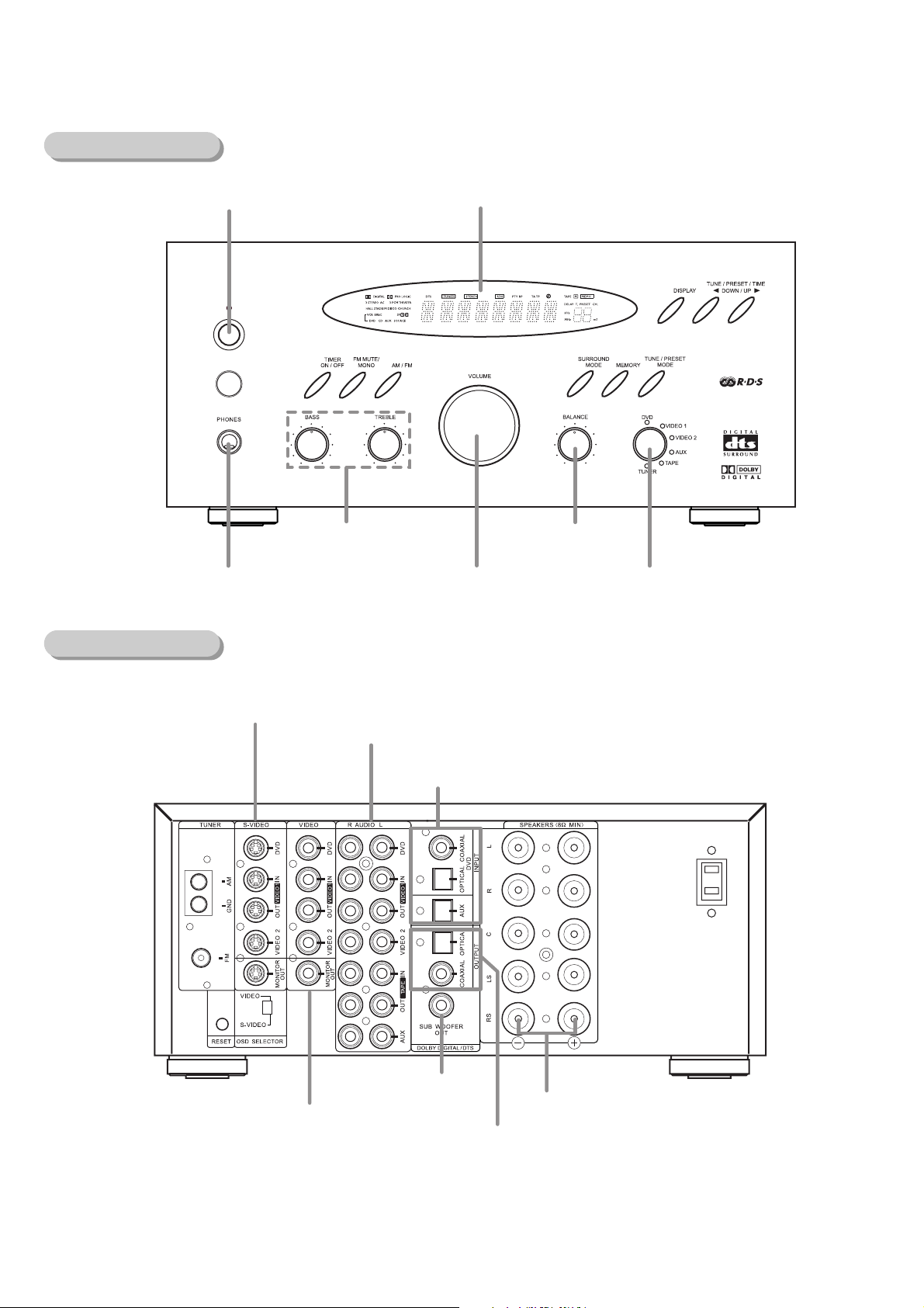
LOCATION OF CUSTOMER CONTROLS
FRONT PANEL
REAR PANEL
POWER STANDBY/ON button
VFL Display
PHONES
S-VIDEO Signal jacks
BASS/TREBLE
Tone Controls
AUDIO Signal jacks
BALANCE
Control
MASTER VOLUME
Control
Dolby Digital / DTS / PCM
DIGITAL IN jacks
SOURCE SELECTOR
Control
(For AH version only)
VIDEO Signal jacks
PRE OUT jack
SPEAKER terminals
DIGITAL OUT jacks
1-8
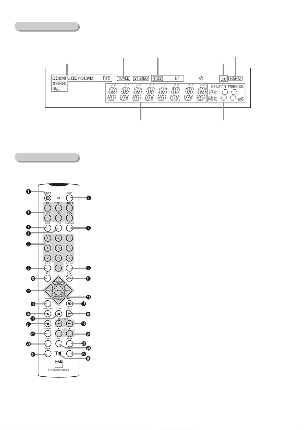
VFL DISPLAY
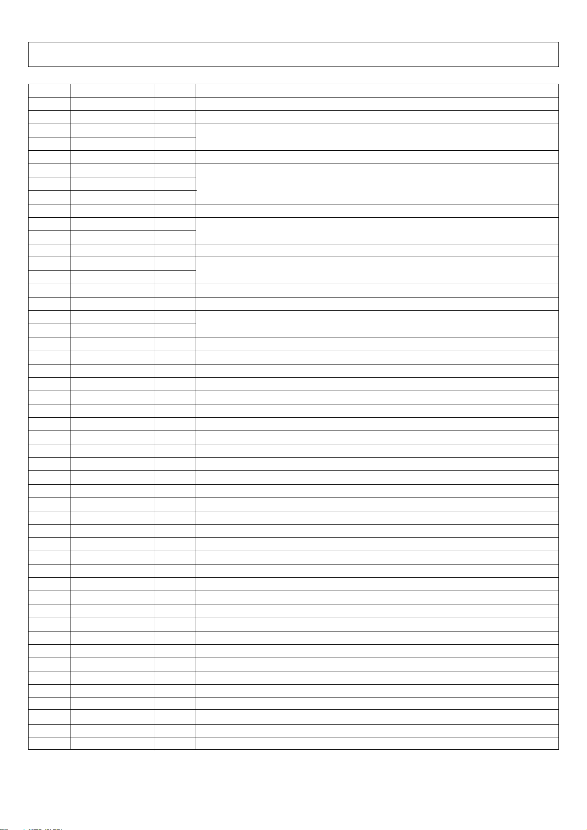
REMOTE CONTROL
1. POWER ON/OFF button (L75/L55)
2. SLEEP button (L75)
3. INPUT SOURCE Selector buttons (L75)
4. SURROUND MODE button (L75)
5. TEST TONE button (L75)
6. NUMERIC button (L75/L55)
7. PROGRAM button (L55)
8. OSD ON/OFF button (L75), DVD SET UP button (L55)
9. DIGITAL INPUT/RDS button (L75), DVD DISPLAY button (L55)
10. TITLE button (L55)
11. MENU buttons (L55)
12. ARROW buttons (L75/55)
VOLUME UP/DOWN, PRESET UP/DOWN buttons (L75)
13. ENTER button (L75/55)
14. RETURN button (L55)
15. MUTE button (L75)
16. OPEN/CLOSE buttons (L55)
17. STOP button (L55)
18. PLAY button (L55)
19. FOR/ REV, SCAN/SKIP button (L55)
20. SLO W buttons (L55)
21. PAUSE/STEP button (L55)
22. REPEAT button (L55)
23. CLEAR button (L55)
24. AUDIO button (L55)
25. ANGLE button (L55)
26. ZOOM button (L55)
27. SUBTITLE button (L55)
28. SWITCH
SURROUND MODE indicator
TUNED indicator
INPUT SOURCE, FREQUENCY,
LEVEL indicator
RDS indicator
TUNER MUTE indicator
MEMORY indicator
DELAY TIME, PRESET
CHANNEL indicator

EXPLODED VIEW
N0
DESCRIPION
1
AL PANEL
2
SIDE BAR
3
VOLUME KNOB ASS'Y
4
VOLUME KNOB ASS'Y(B)
5
VOLUME KNOB ASS'Y(A)
6
7
WINDOW,FIP
8
INDICATOR,POWER
KNOB, DISPLAY
9
10
KNOB, POWER
11
WINDOW, SENSOR
12
PANEL, SUB
13
FAN
14
15
SINK, HEAT(F)
16
CHASSIS , BOTTOM KUA1A190
17
FOOT
18
FOOT CUSHION
19
20
21
PANEL , REAR
22
23
AC CORD
AC CORD BUSHING
24
TOP CABINET
25
26
27
SUB PCB
28
PCB , AUDIO INPUT
29
30
31
32
33
34
35
36
37
38
39
40
41
42
43
44
TRANS , MAIN
45
46
TRANS , SUB
47
TUNER,MODULE
48
MOTOR
KKM1A105ZC26
KKM1A062C26
KGK1A063ZA
KGK1A064ZA
KGK2A064YA
KGU1A244A8
KGL1A188
KBT1A745M7K102
KBT1A756M7K102
KGU1A245A10
KGW1A299
KDD1A013
KMH1A117COVER, FAN
KMY1A116SINK, HEAT(R)
BKL1A060
BHG1A171
KHE170
C:KKF1A212ZK1
AH:KKF2A212YK1
C:BJA2B044Z
AH:BJA523FBY
KHR1A028
KMH1A119
KUP11396-1
KUP11396-2/3 1
KUP11396-4PCB , VIDEO INPUT
KUP11396-5PCB , SVIDEO INPUT
KUP11396-7PCB , GUIDE
KUP11396-1PCB , U-COM
KUP11398 PCB , SURROUND
KUP11397-1PCB , FRONT AMP
KUP11397-2PCB , SURROUND AMP
KUP11431-1PCB , SPEAKER
KUP11431-3PCB , SUB TRANS
KUP11431-2PCB , AC OUTLET
KUP11431-4PCB , CONNRCTOR
KUP11395-1PCB , MAIN
KUP11395-2PCB , TRANS
KUP11395-3PCB , PSU
KUP11396-6PCB , HEADPHONE
C:KLT5V026ZE
AH:KLT5V026ZU
C:KLT5L052ZE
AH:KLT5L052ZU
C:BNVTFCE1E319A
AH:BNVTFCE1U116A
BDMMDN4RB4MRC
51
SCREW
Q,tyPARTS-NO
52
SPECIAL SCREW
1
53
SCREW KTB3+6J
2
54
SCREW
2KHG1A198RUBBER , TRANS
2
55
SCREW
1
56
SCREW
1
57
SCREW
3
58
SPECIAL SCREW
1
59
SCREW
1.2
60
SCREW
3
1
61 KTW3+14JSCREW 4
SCREW
62
1
SCREW
63
1
SCREW
64
1
SCREW
65
1
66
SCREW
1KMY1A115
67 SCREW
1
1
4
4
6KHE1A023PCB MOUNT
1HOLDER, PCB
1
1
1
1KKC1B082S21
12SUPPORT, H/S
10C:KRE1A037LOCKER
1
1
1
1
1
1
1
1
1
1
1
1
1
1
1
1
1
1
1
KTS3+8J
KHD1A016
KTB3+6F
KTB3+10G
KTWS3+10G
KSN2+4
KHD1A012
KTB3+16J
KTB3+8J
KTW3+16J
KTW3+8J
KTB4+6J
KTB3+6JFZ
KTB3+10GFZ
12
4
4
7
7
10
1
2
15
12
8
2
5
4
4KTB4+6FFZ
C:14
C:19
44
AH:13
AH:21
56
33
13
57
x2
62
x2
36
14
60
48
40
58
x4
x9
15
16
25
26
x6
59
35
x6
66
X4
38
65
39
46
X4
22 AH
22
X10
C
39 AH
27
C
X10
66
23
24
X21
67
37
34
29
30
53
45
42
X2
31
X4
43
64
X2
60
X2
61
47
41
x6
58
X2
X2
64
11
10
8
x6
59
X10
55
26
63
x6
32
3
x6
54
9
x2
52
8
x4
4
x3
5
6
7
51
x4
53
2
x2
1
18
19
63
x4
x4
x4
X7
17
21
60
X2
53
x3
1-9 1-10

2-11
SECTION 2
ELECTRICAL CONTENTS
CONTENTS
IC BLOCK DIAGRAMS & PIN DESCRIPTION ........................................................................................ 2-11
1. IC81 (TMP87PS71F u-COM) .............................................................................................................. 2-12
2. IC34 (YSS912C AC3/DTS Decoder) .................................................................................................. 2-14
3. IC84 (NJU3713G EXPANDOR) ........................................................................................................... 2-16
4. IC32 (AK4112VF DIR) ......................................................................................................................... 2-17
5. IC33 (AK4527VQ CODEC) .................................................................................................................. 2-17
6. IC21, 22, 23 (NJU3713G EXPANDOR) ............................................................................................... 2-18
7. IC12~15, 37~42, 82 (OPA2134UA, NJM2068MD, OPAMP) ............................................................... 2-18
8. IC35 (IS61C256A15J 256K SRAM) ..................................................................................................... 2-18
9. IC36 (TC9164AF FUNCTION) ............................................................................................................ 2-19
10. IC36 (TC9163AF FUNCTION) ........................................................................................................... 2-19
11. IC16 (TC9482F ELECTRONIC VOLUME) ........................................................................................ 2-20
12. IC31 (TC74HCUO4AFN INVERTER)................................................................................................ 2-20
13. IC85 (MC74HC14D INVERTER) ........................................................................................................ 2-21
14. IC25 (ANAM2024V OSD).................................................................................................................... 2-21
15. IC83 (SAA6579TV1 ROS FILTER)..................................................................................................... 2-22
16. TRANSISTOR, REGULATOR IC BLOCK DIAGRAM........................................................................ 2-22
DIAGRAMS ................................................................................................................................................ 2-23
1. BLOCK DIAGRAM ................................................................................................................................ 2-23
2. WIRING DIAGRAM .............................................................................................................................. 2-27
3. SCHEMATIC DIAGRAM ...................................................................................................................... 2-29
MAIN............................................................................................................................................2-29
FRONT ........................................................................................................................................2-31
INPUT..........................................................................................................................................2-33
AMP/ SPEAKER .........................................................................................................................2-35
SURROUND ...............................................................................................................................2-37
4. PRINTED CIRCUIT BOARDS ............................................................................................................. 2-41
MAIN ...........................................................................................................................................2-41
FRONT/ INPUT ...........................................................................................................................2-43
AMP/ SPEAKER .........................................................................................................................2-45
SURROUND ...............................................................................................................................2-47
2-12
PIN No. SYMBOL I/O DESCRIPTION
1
2
3
4
5
6
7
8
9
10
11
12
13
14
15
16
17
18
19
20
21
22
23
24
25
26
27
28
29
30
31
32
33
34 ~ 35
36 ~ 43
44 ~ 65
66
67
68
69
70
71
72
73
74
75, 76
77, 78
79
80
-
REMOTE IN
RDS CLK
RDS DATA
Function Mute
EVOL Data
EVOL CLK
EVOL CE (STB)
Vpp (Test)
XIN
XOUT
RESET
X IN
X OUT
Vss (GND)
Back Up
Function SW 2
Function SW 1
Power ON
YSS912 DIN
OSD CS
Surr./OSD CLK
YSS912 CS
Surr./OSD Data
AK4112 CS
YSS912 CSBN
YSS912 RESET
PLL Data In
Func. STB
CLK 3
DATA 3
PLL CE
VDD/VCC
Option/VFL Grid
VFL Grid
FIP Segment
Vkk
Option
Protect IN
Stereo IN
Tuned IN
OSD IN
Hphone IN
Video Mute
SP ON/OFF
Volume (Encoder)
KEY Matrix
STB
Tuner Mute
-
I
O
I
O
O
O
O
-
I
O
I
I
O
I
I
I
I
O
O
O
O
O
O
O
O
O
I
O
O
O
O
-
O
O
O
-
I
I
I
I
I
I
O
I
I
I
O
O
Not Use (No connection)
Remote Control Sensor Data Input
RDS IC (SA6579TV1) CLK/Data Port
Function Mute Control Output port (Active “H”)
Electronic Vol. IC (TC9482F) Data/CLK/STB Port
Program Supply Voltage (GND Connection)
32.788KHz Crystal Connection Port
Reset Input Port (“L”)
8MHz Cystal Connection Port
Device GND Port
Back Up Mode Control Port (“L”)
Function Selector (ENCODER) Control port
Power ON Control port (Active “L”)
YSS912 Data Input Ports
ODS IC (ANAM2024V) Chip Selector Port
Surr./OSD CLK Output port
Chip Selector port for YSS912
Surr./OSD Data Output Port
Chip Selector Port for AK4112
Sub DSP Chip Selector for YSS912
Reset (Initial Clear) Port for YSS912
PLL IC (LC72131) Data Input Port
Func. IC (KIC9163/64) Strobe Control Port
Func./PLL IC CLK Control Port
Func./PLL IC Data Control Port
PLL IC (LC72131) Chip Enable Control Port
Power Supply Port (+5V)
Option Control Port/ VFL Grid Control Port
VFL Grid Control Port
VFL Segment Control Port
VFL Power Supply Port (-30V)
Option Control Port
Protect Input Port (“L”)
Stereo Display Control Port (“L”)
Tuned Display Control Port (“L”)
ODS Input Control Port
Headphone In/ Out Defect Port
Videon Mute Control Port (“L”)
Speaker ON/OFF Control Port
Master Volume Up/Down Control Port
Key Control Input Port
Extended IC (NJU3713G) Strobe Control Port
Tuner Mute Control Port
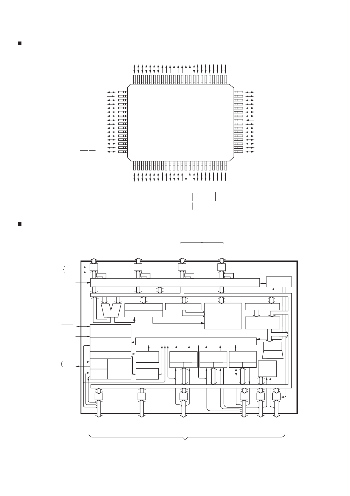
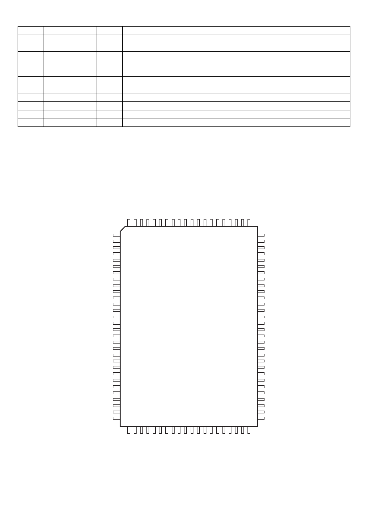
IC PIN FUNCTION (IC81 : TMP87PS71F-ANAM 1328AT OTP, UCOM)
2-13
u-COM IC PIN ASSIGNMENT & BLOCK DIAGRAM
PIN ASSIGNMENTS
(TOP VIEW)
BLOCK DIAGRAM
(CIN5/KEY6) P46
(CIN4/KEY7) P47
(PWM/PDO) P55
(SIS) P97
VKK
(KEY0) P40
(KEY1) P41
(KEY2) P42
(KEY3) P43
(KEY4) P44
(KEY5) P45
(CIN3) P50
(CIN2) P51
(CIN1) P52
(CIN0) P53
P54
P96 (S14)
P95 (S13)
P94 (S12)
P93 (S11)
P92 (S10)
P91 (S9)
P90 (S8)
P87 (S7)
P86 (S6)
P85 (S5)
P84 (S4)
P83 (S3)
P82 (S2)
P81 (S1)
P80 (S0)
P77 (G0)
P76 (G1)
P75 (G2)
P74 (G3)
P73 (G4)
P72 (G5)
65
66
67
68
69
70
71
72
73
74
75
76
77
78
79
80
123456789101112131415161718192021222324
(INT1) P11
(INT0) P10
(DVO) P13
(INT2/TC1) P12
55565758596061626364 54 53 52 51 50 49 48 47 46 45 44 43 42 41
TEST
(XTIN) P21
(XTIN) P22
XIN
RESET
XOUT
P14
P16
(TC2) P15
P17
VSS
(TC4) P31
(INT3/TC3) P30
(INTS/STOP) P20
(SI) P33
(SO) P34
(SCK) P32
P71 (G6)
P70 (G7)
P67 (G8)
40
39
38
37
36
35
34
33
32
31
30
29
28
27
26
25
P36
(HSO) P37
(HSCK) P35
P66 (G9)
P65 (G10)
P64 (G11)
P63 (G12)
P62 (G13)
P61 (G14)
P60 (G15)
VDD
P07
P06
P05
P04
P03
P02
P01
P00
Power Supply
VFT Power
Supply
Reset I/O
Test Pin
Resonator
connecting
Pins
VDD
VSS
VKK
RESET
TEST
XIN
XOUT
I/O Ports
P97
to
P90
P9
ALU
System Controller
Standby Controller
Timing Generator
High
frequ.
Low
frequ.
P2
Clock
Generator
Output Ports
P87
to
P80
P8
VFT drive circuit (automatic display)
Stack PointerP S W
Flags
RBS
Time Base
Timer
Timer/Counters
TC1 TC2 TC3 TC4 SIO HSO
Watchdog
Timer
P0
I/O Ports
P77
to
P70
P7
Interrupt Controller
16-bit
Timer/Counters
P1
P67
to
P60
P6
Data Memory
(RAM)
Register banks
8-bit
Program counter
Program Memory
Serial
Interfaces
P3
(ROM)
Register
Decoder
6-bit A/D
Converter
P5
Key scan
control
Inst.
Inst.
P4
P22
to
P20
P07
to
P00
P17
to
P10
I/O Ports
P37
to
P30
P55
to
P50
P47
to
P40
2-14
PIN No. SYMBOL I/O DESCRIPTION
1,31,71
2
3
4
5
6
7
8
9
10, 20
11
12
13
14
15
16
17
18
19
20
21,41,51,81,91
22
23
24
25 ~ 29
32
33 ~ 39
40,50,60,80,90,100
42 ~ 44
45 ~ 47
48
49
52
53
54
55
56
57
58
59
61
62
63
64
65
66
67
68
69
VDD1
RAMCEN
RAMA16
RAMA15
SDIB0
SDIB1
SDIB2
XI
XO
VSS
AVDD
SDIB3
TEST
TEST
OVFB
DTSDATA
AC3DATA
SDOB3
CPO
AVSS
VDD2
SDOA2
SDOA1
SDOA0
RAMA 14~10
OPORT 0
OPORT 1~7
VSS
RAAM 9~7
SDOB 2~0
SDBCK1
SDWCK1
NONPCM
CRC
MUTE
KARAOKE
SURENC
/SDBCK 0
RAMA6
RAMA5
RAMA4
/IC
TEST
RAMA3
/CSB
/CS
SO
SI
SCK
-
O
O
O
I+
I+
I+
I+
O
-
-
I+
-
-
O
O
O
O
A
-
-
O
O
O
O
O
O
-
O
O
I+
I+
O
O
O
O
O
O
O
O
O
Is
-
O
Is+
Is
Ot
Is
Is
+5V Power Supply(for I/Os)
External SRAM interface /CE
External SRAM interface address 16 (not use)
External SRAM interface address 15 (not use)
PCM input 0 to Sub DSP(not use)
PCM input 1 to Sub DSP(not use)
PCM input 2 to Sub DSP(not use)
Crystal oscillator connection(12.288MHz)
Ground
+3.3V power supply (for PLL circuit)
PCM input 3 to Sub DSP (not use)
Test terminal(to be open in normal use)
Test terminal(to be open in normal use)
Detection of overflow at Sub DSP (not use)
Detection of DTS data (not use)
Detection of AC-3 data (not use)
PCM output from Sub DSP (not use)
Output terminal for PLL,to be connected to ground through the external analog filter circuit
Ground for PLL circuit)
+3.3V power supply (for core logic)
PCM output from Main DSP (C,LFE) (not use)
PCM output from Main DSP (LS,RS) (not use)
PCM output from Main DSP (L,R) (not use)
External SRAM interface address 14~10
Output port for general purpose
Output port for general purpose (not use)
Ground
External SRAM interface address 9~7
PCM output from Sub DSP
Bit clock input for SDOA,SDIB,SDOB (not use)
Word clock input for SDOA,SDIB,SDOB (not use)
Detection of non-PCM data (not use)
Detection of AC-3 CRC error (not use)
Detection of auto mute (not use)
Detection of AC-3 karaoke data (not use)
Detection of AC-3 2/0 mode Dolby surround encoded input (not use)
Inverted SDBCK0 clock output (not use)
External SRAM interface address 6
External SRAM interface address 5
External SRAM interface address 4
Initial clear
Test terminal (to be open in normal use)
External SRAM interface address 3
Sub DSP Chip select
Microprocessor interface Chip select input
Microprocessor interface serial data output
Microprocessor interface /Sub DSP Serial data input
Microprocessor interface /Sub DSP clock input
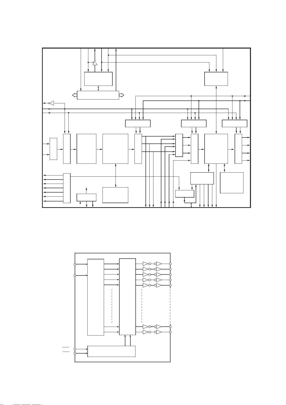
AC 3/DTS DECODER (YSS912C:IC34)
2-15
PIN No. SYMBOL I/O DESCRIPTION
70
72 ~ 79
82
83
84
85
86
87
88
89
92 ~ 99
RAMA2
RAMD0~7
SDWCK0
SDBCK0
SDIA0
SDIA1
RAMA1
RAMA0
RAMWEN
RAMOEN
IPORT7~0
O
I+/O
I
I
I
I
O
O
O
O
I+
External SRAM interface address 2
External SRAM interface data (STREAM0~7 output when External SRAM is not in use)
Word clock input for SDIA, SDOA, SDIB, SDOB
Bit clock input for SDIA,SDOA,SDIB,SDOB
AC-3 Bitstream (or PCM) data input for Main DSP
AC-3 Bitstream (or PCM) data input for Main DSP
External SRAM interface address 1
External SRAM interface address 0
External SRAM interface /WE
External SRAM interface /OE
Input port for general purpose (not use)
NOTE) Is: Schmidt trigger input terminal It: Input terminal with pull-up resistor
O: Digital output terminal Ot: Tri-state digital output terminal
A: Analog terminal
YSS912C PIN CONFIGURATION
VSSIPORT0
IPORT1
IPORT2
IPORT3
IPORT4
IPORT5
IPORT6
IPORT7
VDD2
VSS
RAMOEN
RAMWEN
RAMA0
RAMA1
SDIA1
SDIA0
SDBCK0
SDWCK0
VDD2
VDD1
RAMCEN
RAMA16
RAMA15
SDIB0
SDIB1
SDIB2
XO
VSS
AVDD
SDIB3
TEST
TEST
OVFB
DTSDATA
AC3DATA
SDOB3
CPO
AVSS
VDD2
SDOA2
SDOA1
SDOA0
RAMA14
RAMA13
RAMA12
RAMA11
RAMA10
VSS
100 99 98 97 96 95 94 93 92 91 90 89 88 87 86 85 84 83 82 81
1
2
3
4
5
6
7
XI
8
9
10
11
12
13
14
15
16
17
18
19
20
21
22
23
24
25
26
27
28
29
30
31 32 33 34 35 36 37 38 39 40 41 42 43 44 45 46 47 48 49 50
VSS
80
RAMD7
79
RAMD6
78
77
RAMD5
RAMD4
76
RAMD3
75
RAMD2
74
RAMD1
73
RAMD0
72
VDD1
71
RAMA2
70
SCK
69
SI
68
SO
67
/CS
66
/CSB
65
RAMA3
64
TEST
63
/IC
62
RAMA4
61
60
VSS
59
RAMA5
58
RAMA6
57
/SDBCK0
56
SURENC
55
KARAOKE
MUTE
54
CRC
53
NONPCM
52
51
VDD2
VDD1
VSS
VDD2
OPORT0
OPORT1
OPORT2
OPORT3
OPORT4
OPORT5
OPORT6
OPORT7
RAMA9
RAMA8
RAMA7
SDOB2
SDOB1
SDOB0
SDBCK1
SDWCK1
VSS
2-16
IPORT 0~7
YSS912C BLOCK DIAGRAM
NJU3713G (EXPANDOR IC 84)
/CS
SO
OPORT 0~7
SCK
SI
/CSB
SCK
SI
/SDBCK0
SDBCK0
SDWCK0
SDIA0
SDIA1
SURENC
KARAOKE
MUTE
CRC
AC3DATA
DTSDATA
NONPCM
SDIASEL
SDIA Interface SDIA Interface
STREAM 0~7
Operating clock
Microprocessor
Interface
Control Registers
Input Buffer
(30MHz)
PLL
CPO
XO
XI
Control SignalsControl Signals
AC-3/Pro Logic/DTS
Main DSP
decoder
24 * 16
Delay RAM
L,R
SDOA Interface
LS,RS
SDOA0
C, LFE
SDOA2
SDOA1
SDIB1
SDIB0
SDIB3
SDIB2
SDIBSEL
ERAMUSE
RAMA 0~7
Coefficient
Program RAM
SDIB Interface
External RAM
interface
RAMOEN
RAMWEN
RAMCEN
Sub DSP
24 * 16
OVFB
RAMA 0~16
SDOBCKSELSDOBCKSELSDOACKSEL
Data RAM
SDBCK1
SDWCK1
SDOB Interface
SDOB0
SDOB1
SDOB2
SDOB3
DATA
CLK
STB
CLR
10
11
12
13
Shift Circuit
Controller Circuit
Latch Circuit
17
8
9
14
15
16
P1
P2
P3
P4
1
P5
P11
P12
 Loading...