

NAD L73 Service Manual

SERVICE MANUAL
L73
DVD RECEIVER
L73
DVD RECEIVER

1-3
SECTION 1
SUMMARY
CONTENTS
PRODUCT SAFETY SERVICING GUIDELINES.......................................................................................... 1-4
SERVICING PRECAUTIONS ....................................................................................................................... 1-5
* General Servicing Precautions
* Insulation checking prodedure
* Electrostatically Sensitive Devices
SPECIFICATIONS ......................................................................................................................................... 1-6
DISASSEMBLY .............................................................................................................................................. 1-7
PRINCIPAL PART LOCATION ...................................................................................................................... 1-8
EXPLODED VIEW ............................................................................................................................. 1-9 ~ 1-13

1-4
PRODUCT SAFETY SERVICING GUIDELINES
CAUTION : DO NOT ATTEMPT TO MODIFY THIS PRODUCT IN
ANY WAY. NEVER PERFORM CUSTOMIZED INSTALLATIONS
WITHOUT MANUFACTURER’S APPROVAL. UNAUTHORIZED
MODIFICATIONS WILL NOT ONLY VOID THE WARRANTY, BUT
MAY LEAD TO YOUR BEING LIABLE FOR ANY RESULTING
PROPERTY DAMAGE OR USER INJURY.
SERVICE WORK SHOULD BE PERFORMED ONLY AFTER YOU
ARE THOROUGHLY FAMILIAR WITH ALL OF THE FOLLOWING
SAFETY CHECKS AND SERVICING GUIDELINES. TO DO
OTHERWISE, INCREASES THE RISK OF POTENTIAL HAZARDS
AND INJURY TO THE USER.
WHILE SERVICING, USE AN ISOLATION TRANSFORMER FOR
PROTECTION FROM AC LINE SHOCK.
SAFETY CHECKS
AFTER THE ORIGINAL SERVICE PROBLEM HAS BEEN
CORRECTED. A CHECK SHOULD BE MADE OF THE
FOLLOWING.
SUBJECT : FIRE & SHOCK HAZARD
1. BE SURE THAT ALL COMPONENTS ARE POSITIONED IN
SUCH A WAY AS TO AVOID POSSIBILITY OF ADJACENT
COMPONENT SHORTS. THIS IS ESPECIALLY IMPORTANT
ON THOSE MODULES WHICH ARE TRANSPORTED TO AND
FROM THE REPAIR SHOP.
2. NEVER RELEASE A REPAIR UNLESS ALL PROTECTIVE
DEVICES SUCH AS INSULATORS, BARRIERS, COVERS,
SHIELDS, STRAIN RELIEFS, POWER SUPPLY CORDS, AND
OTHER HARDWARE HAVE BEEN REINSTALLED PER
ORIGINAL DESIGN. BE SURE THAT THE SAFETY PURPOSE
OF THE POLARIZED LINE PLUG HAS NOT BEEN DEFEATED.
3. SOLDERING MUST BE INSPECTED TO DISCOVER POSSIBLE
COLD SOLDER JOINTS, SOLDER SPLASHES OR SHARP
SOLDER POINTS. BE CERTAIN TO REMOVE ALL LOOSE
FOREIGN PARTICLES.
4. CHECK FOR PHYSICAL EVIDENCE OF DAMAGE OR
DETERIORATION TO PARTS AND COMPONENTS. FOR
FRAYED LEADS, DAMAGED INSULATION (INCLUDING AC
CORD). AND REPLACE IF NECESSARY FOLLOW ORIGINAL
LAYOUT, LEAD LENGTH AND DRESS.
5. NO LEAD OR COMPONENT SHOULD TOUCH A RECEIVING
TUBE OR A RESISTOR RATED AT 1 WATT OR MORE. LEAD
TENSION AROUND PROTRUDING METAL SURFACES MUST
BE AVOIDED.
6. ALL CRITICAL COMPONENTS SUCH AS FUSES,
FLAMEPROOF RESISTORS, CAPACITORS, ETC. MUST BE
REPLACED WITH EXACT FACTORY TYPES, DO NOT USE
REPLACEMENT COMPONENTS OTHER THAN THOSE
SPECIFIED OR MAKE UNRECOMMENDED CIRCUIT
MODIFICATIONS.
7. AFTER RE-ASSEMBLY OF THE SET ALWAYS PERFORM AN
AC LEAKAGE TEST ON ALL EXPOSED METALLIC PARTS OF
THE CABINET, (THE CHANNEL SELECTOR KNOB, ANTENNA
TERMINALS. HANDLE AND SCREWS) TO BE SURE THE SET
IS SAFET TO OPERATE WITHOUT DANGER OF ELECTRICAL
SHOCK. DO NOT USE A LINE ISOLATION TRANSFORMER
DURING THIS TEST USE AN AC VOLTMETER, HAVING 5000
OHMS PER VOLT OR MORE SENSITIVITY, IN THE
FOLLOWING MANNER; CONNECT A 1500 OHM 10 WATT
RESISTOR, PARALLELED BY A .15 MFD, 150V AC TYPE
CAPACITOR BETWEEN A KNOWN GOOD EARTH GROUND
(WATER PIPE, CONDUIT, ETC.) AND THE EXPOSED
METALLIC PARTS, ONE AT A TIME.
MEASURE THE AC VOLTAGE ACROSS THE COMBINATION
OF 1500 OHM RESISTOR AND .15 MFD CAPACITOR.
REVERSE THE AC PLUG AND REPEAT AC VOLTAGE
MEASUREMENTS FOR EACH EXPOSED METALLIC PART.
VOLTAGE MEASURE MUST NOT EXCEED 75 VOLTS R.M.S.
THIS CORRESPONDS TO 0.5 MILLIAMP AC ANY VALUE
EXCEEDING THIS LIMIT CONSTITUTES A POTENTIAL
SHOCK HAZARD AND MUST BE CORRECTED IMMEDIATELY.
SUBJECT : GRAPHIC SYMBOLS
SUBJECT : TIPS ON PROPER INSTALLATION
1. NEVER INSTALL ANY PRODUCT IN A CLOSED-IN RECESS,
CUBBYHOLE OR CLOSELY FITTING SHELF SPACE. OVER
OR CLOSE TO HEAT DUCT, OR IN THE PATH OF HEATED
AIR FLOW.
2. AVOID CONDITIONS OF HIGH HUMIDITY SUCH AS:
OUTDOOR PATIO INSTALLATIONS WHERE DEW IS A
FACTOR, NEAR STEAM RADIATORS WHERE STEAM
LEAKAGE IS A FACTOR, ETC.
3. AVOID PLACEMENT WHERE DRAPERIES MAY OBSTRUCT
REAR VENTING. THE CUSTOMER SHOULD ALSO AVOID THE
USE OF DECORATIVE SCARVES OR OTHER COVERINGS
WHICH MIGHT OBSTRUCT VENTILATION.
4. WALL AND SHELF MOUNTED INSTALLATIONS USING A
COMMERCAL MOUNTING KIT MUST FOLLOW THE FACTORY
APPROVED MOUNTING INSTRUCTIONS A PRODUCT
MOUNTED TO A SHELF OR PLATFORM MUST RETAIN ITS
ORIGINAL FEET (OR THE EQUIVALENT THICKNESS IN
SPACERS) TO PROVIDE ADEQUATE AIR FLOW ACROSS
THE BOTTOM, BOLTS OR SCREWS USED FOR FASTENERS
MUST NOT TOUCH ANY PARTS OR WIRING. PERFORM
LEAKAGE TEST ON CUSTOMIZED INSTALLATIONS.
5. CAUTION CUSTOMERS AGAINST THE MOUNTING OF A
PRODUCT ON SLOPING SHELF OR A TILTED POSITION,
UNLESS THE PRODUCT IS PROPERLY SECURED.
6. A PRODUCT ON A ROLL-ABOUT CART SHOULD BE STABLE
ON ITS MOUNTING TO THE CART. CAUTION THE
CUSTOMER ON THE HAZARDS OF TRYING TO ROLL A CART
WITH SMALL CASTERS ACROSS THRESHOLDS OR DEEP
PILE CARPETS.
7. CAUTION CUSTOMERS AGAINST THE USE OF A CART OR
STAND WHICH HAS NOT BEEN LISTED BY UNDERWRITERS
LABORATORIES, INC. FOR USE WITH THEIR SPECIFIC
MODEL OF TELEVISION RECEIVER OR GENERICALLY
APPROVED FOR USE WITH T.V.’S OF THE SAME OR
LARGER SCREEN SIZE.
8. CAUTION CUSTOMERS AGAINST THE USE OF EXTENSION
CORDS, EXPLAIN THAT A FOREST OF EXTENSIONS
SPROUTING FROM A SINGLE OUTLET CAN LEAD TO
DISASTROUS CONSEQUENCES TO HOME AND FAMILY.
THE LIGHTNING FLASH WITH ARROWHEAD SYMBOL, WITHIN AN
EQUILATERAL TRIANGLE, IS INTENDED TO ALERT THE USER TO THE
PRESENCE OF UNINSULATED “DANGEROUS VOLTAGE” WITHIN THE
PRODUCT’S ENCLOSURE THAT MAY BE OF SUFFICIENT MAGNITUDE TO
CONSTITUTE A RISK OF ELECTRIC SHOCK.
THE EXCLAMATION POINT WITHIN AN EQUILATERAL TRIANGLE IS
INTENDED TO ALERT THE USER TO THE PRESENCE OF IMPORTANT
OPERATING AND MAINTENANCE (SERVICING) INSTRUCTIONS IN THE
LITERATURE ACCOMPANYING THE APPLIANCE.

1-5
SERVICING PRECAUTIONS
CAUTION : Before servicing the A/V Receiver covered by this
service data and its supplements and addends, read and follow the
SAFETY PRECAUTIONS. NOTE : if unforeseen circumstances
create conflict between the following servicing precautions and any
of the safety precautions in this publication, always follow the safety
precautions.
Remember Safety First:
General Servicing Precautions
1. Always unplug the A/V Receiver AC power cord from the AC
power source before:
(1) Removing or reinstalling any component, circuit board,
module, or any other assembly.
(2) Disconnecting or reconnecting any internal electrical plug or
other electrical connection.
(3) Connecting a test substitute in parallel with an electrolytic
capacitor.
Caution : A wrong part substitution or incorrect polarity installation
of electrolytic capacitors may result in an explosion hazard.
2. Do not spray chemicals on or near this A/V Receiver or any of its
assemblies.
3. Unless specified otherwise in this service data, clean electrical
contacts by applying an appropriate contact cleaning solution to
the contacts with a pipe cleaner, cottontipped swab, or
comparable soft applicator.
Unless specified otherwise in this service data, lubrication of
contacts is not required.
4. Do not defeat any plug/socket B+ voltage interlocks with which
instruments covered by this service manual might be equipped.
5. Do not apply AC power to this A/V Receiver and/or any of its
electrical assemblies unless all solid-state device heat sinks are
correctly installed.
6. Always connect test instrument ground lead to the appropriate
ground before connecting the test instrument positive lead. Always
remove the test instrument ground lead last.
Insulation Checking Procedure
Disconnect the attachment plug from the AC outlet and turn the
power on. Connect an insulation resistance meter(500V) to the
blades of the attachment plug. The insulation resistance between
each blade of the attachment plug and accessible conductive parts
(Note 1) should be more than 1M-ohm.
Note 1 : Accessible Conductive Parts including Metal panels, Input
terminals, Earphone jacks, etc.
Electrostatically Sensitive (ES) Devices
Some semiconductor (solid state) devices can be damaged easily by
static electricity. Such components commonly are called
Electrostatically Sensitive (ES) Devices. Examples of typical Es
devices are integrated circuits and some field effect transistors and
semiconductor chip components.
The following techniques should be used to help reduce the
incidence of component damage caused by static electricity.
1. Immediately before handling any semiconductor component or
semiconductor-equipped assembly, drain off any electrostatic
charge on your body by touching a known earth ground.
Alternatively, obtain and wear a commercially available
discharging wrist strap device, which should be removed for
potential shock reasons prior to applying power to the unit under
test.
2. After removing an electrical assembly equipped with ES devices,
place the assembly on a conductive surface such as aluminum
foil, to prevent electrostatic charge buildup or exposure of the
assembly.
3. Use only a grounded-tip soldering iron to solder or unsolder ES
devices.
4. Use only an antistatic solder removal device. Some solder
removal devices not classified a “anti-static” can generate
electrical charges sufficient to damage ES devices.
5. Do not use freonpropelled chemicals. These can generate
electrical charge sufficient to damage ES devices.
6. Do not remove a replacement ES device from its protective
package until immediately before you are ready to install it. (Most
replacement ES devices are packaged with leads electrically
shorted together by conductive foam, aluminum foil, or
comparable conductive material).
7. lmmediately before removing the protective material from the
leads of a replacement ES device, touch the protective material to
the chassis or circuit assembly into which the device will be
installed.
Caution : Be sure no power is applied to the chassis or circuit, and
observe all other safety precautions.
8. Minimize bodily motions when handing unpackaged replacement
ES devices. (Normally harmless motion such as the brushing
together of your clothes fabric or the lifting of your foot from a
carpeted floor can generate static electricity sufficient to damage
an ES device.)

1-6
SPECIFICATIONS
Amplifier Section
Output Power (Front) :
F.T.C Rating:
60 watts RMS per channel minimum, both channels
driven into 8 ohms from 20 Hz to 20kHz with no
more than 0.09% total harmonic distortion
Surround Output Power (0.5% THD, 1 kHz, 8 ohms) :
50 + 50 Watt (Front)
50 Watt (Center)
50 + 50 Watt (Rear)
Total Harmonic Distortion (Front) :
0.05 % (at 30 watts, 1 kHz)
Delay Time :
DOLBY DIGITAL : REAR : 0 - 15 ms
CENTER : 0 - 5 ms
DOLBY PRO LOGIC : REAR : 15 - 30 ms
Audio Input Sensitivity/Impedance :
*LINE : 320 mV/47 k ohms
Output Level / Impedance :
VCR REC : 300 mV/2.2 k ohms
Frequency Response :
*LINE : 10 Hz - 60 kHz, +1/ -3 dB
Signal-to-Noise Ratio : 1 Watt
*LINE : 70 dB (IHF-A)
Tone Control :
BASS : ±10 dB at 100 Hz
TREBLE : ±10 dB at 10 kHz
Digital Audio Section
Sampling Frequency :
32 kHz, 44.1 kHz, 48 kHz, 96 kHz
DIGITAL Input Level/Impedance
COAXIAL : 0.5 Vp-p/75 ohms
OPTICAL : -15 dBm ~ -21 dBm
Video Section
Input Sensitivity /Impedance : 1.0 Vp-p/75 ohms
Output Level /Impedance : 1.0 Vp-p/75 ohms
*LINE means CABLE/SAT, VCR, VIDEO4
•
Improvements may result in specifications and features
changing without notice.
•
lllustrations may differ slightly from production models.
FM Tuner Section
(Without notes 100.1 MHz, 65 dBf)
Tuning Range :
87.5 MHz - 108.0 MHz C: 50 kHz steps
AH: 100 kHz steps
AM Suppression Ratio: C: 50 dB
AH: 60 dB
Total Harmonic Distortion (1 kHz) :
Mono : 0.4%
Stereo : 0.5%
Frequency Respones : 20 Hz - 15 kHz, +1/ -1. 5 dB
Stereo Separation (1 kHz) : C: 40 dB
AH: 35 dB
Signal-to-Noise Ratio :
Mono : 70 dB
Stereo : 65 dB
AM Tuner Section
Tuning Range:
C : 522 kHz - 1,620 kHz (9 kHz steps)
AH : 520 kHz - 1,710 kHz (10 kHz steps)
Usable Sensitivity : 55 dB/m
Total Harmonic Distortion : 0.1% at 85 dB/m
Signal-to-Noise Ratio : 40 dB at 85 dB/m
General
Power Requirements :
C : 230V AC, 50Hz
AH : 120V AC, 60Hz
Power Consumption : C: 1.3A
AH: 2.5A
AC Outlets : unswitched x 1, Total 100 W max. (1A)
Dimensions (W x H x D) : 435 x 133 x 375
Weight (net) : 11.8kg
1-7
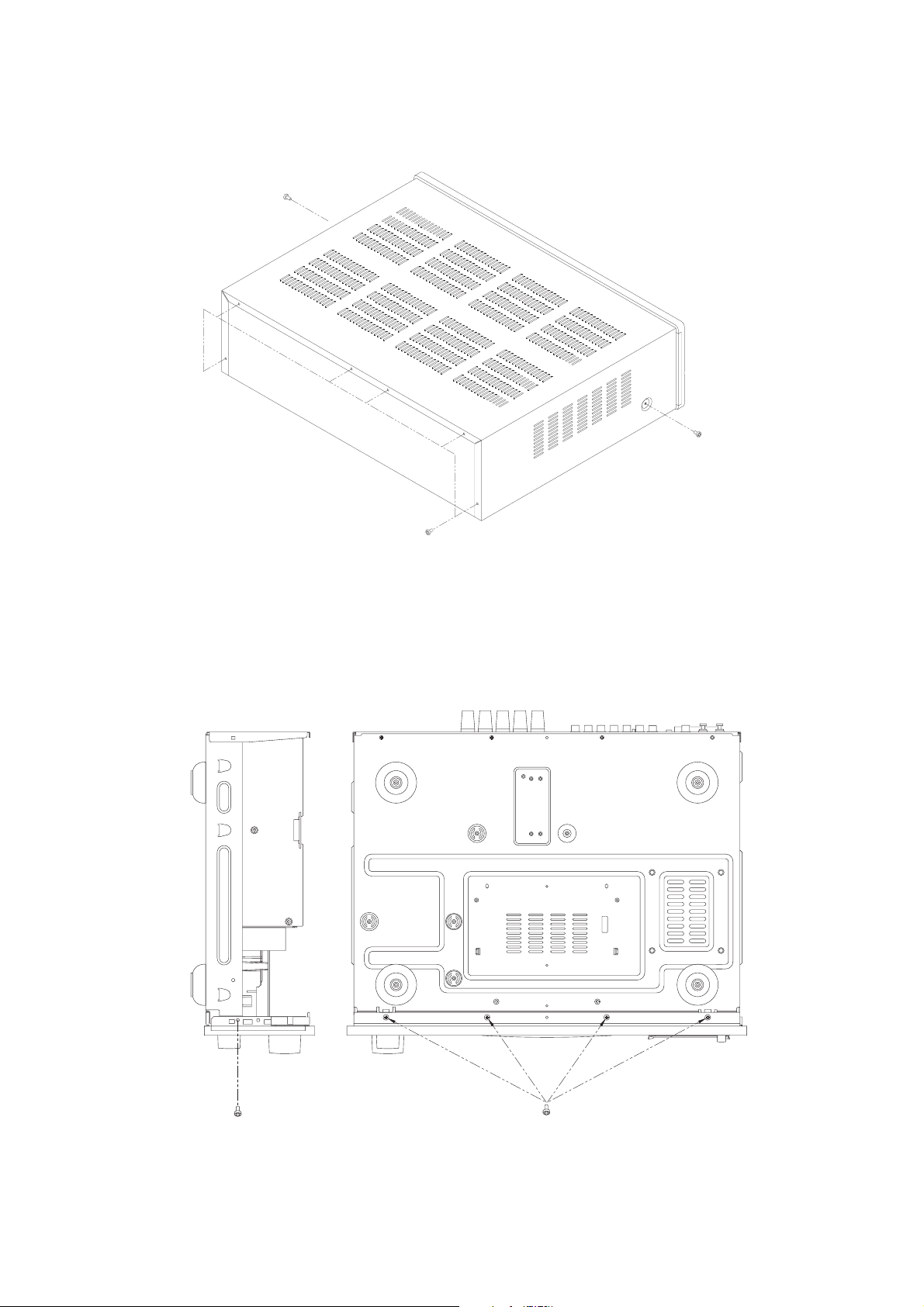
DISASSEMBLY
1> REMOVAL OF TOP COVER
2> REMOVAL OF FRONT PANEL
1-8
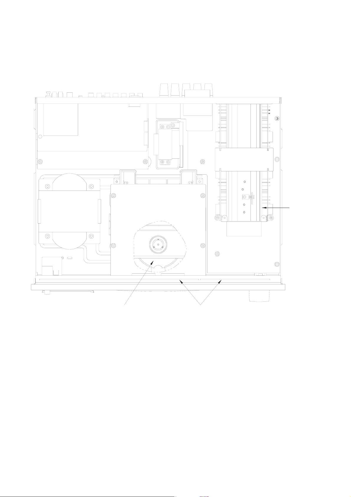
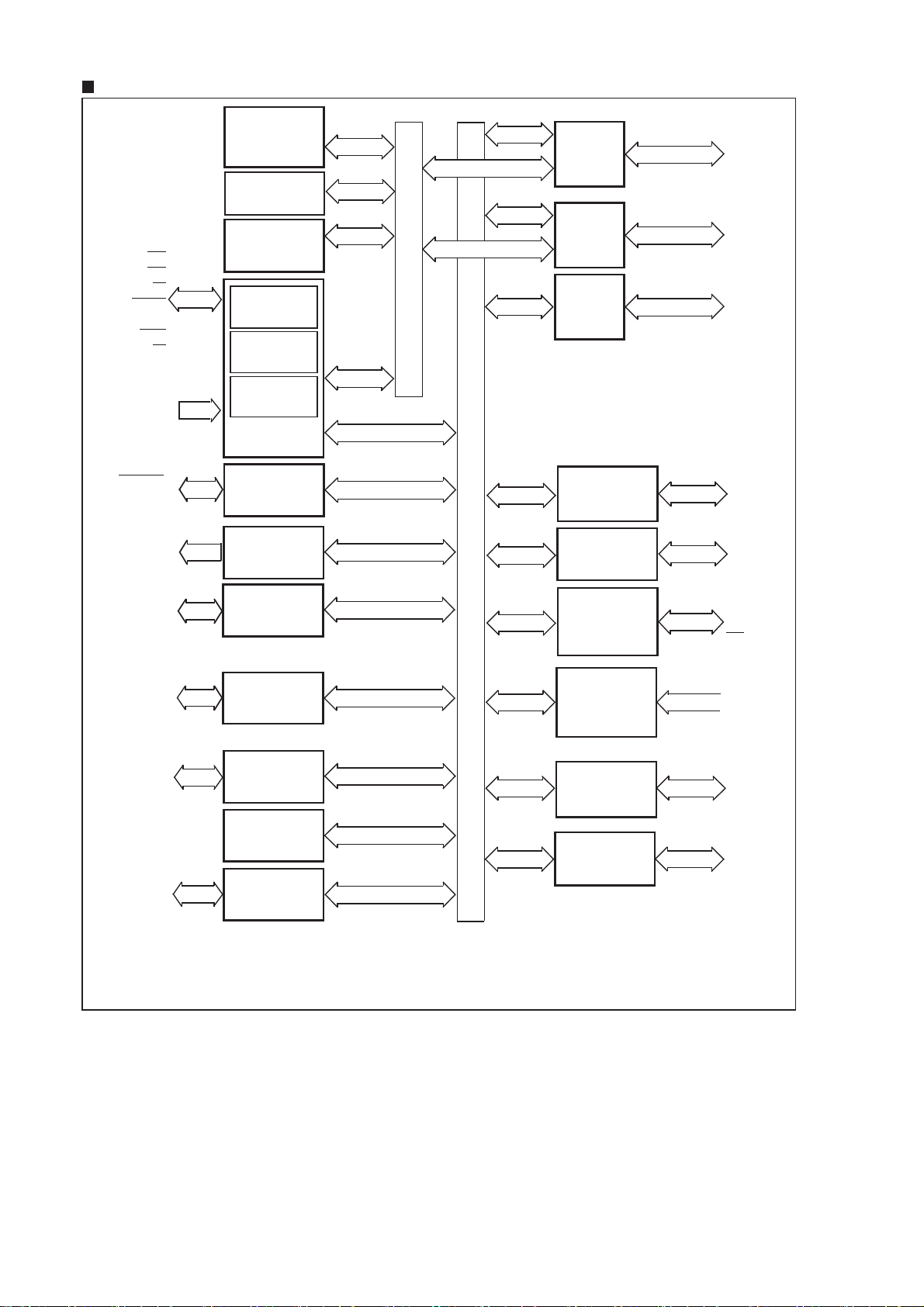
PRINCIPAL PARTS LOCATION
TUNER
PACK
INPUT, DSP, PCB
VIDEO PCB
TRANSFORMER
MICOM PCB
HEATSINK
FAN
POWER PCB
FRONT PCBDVD MECHANISM
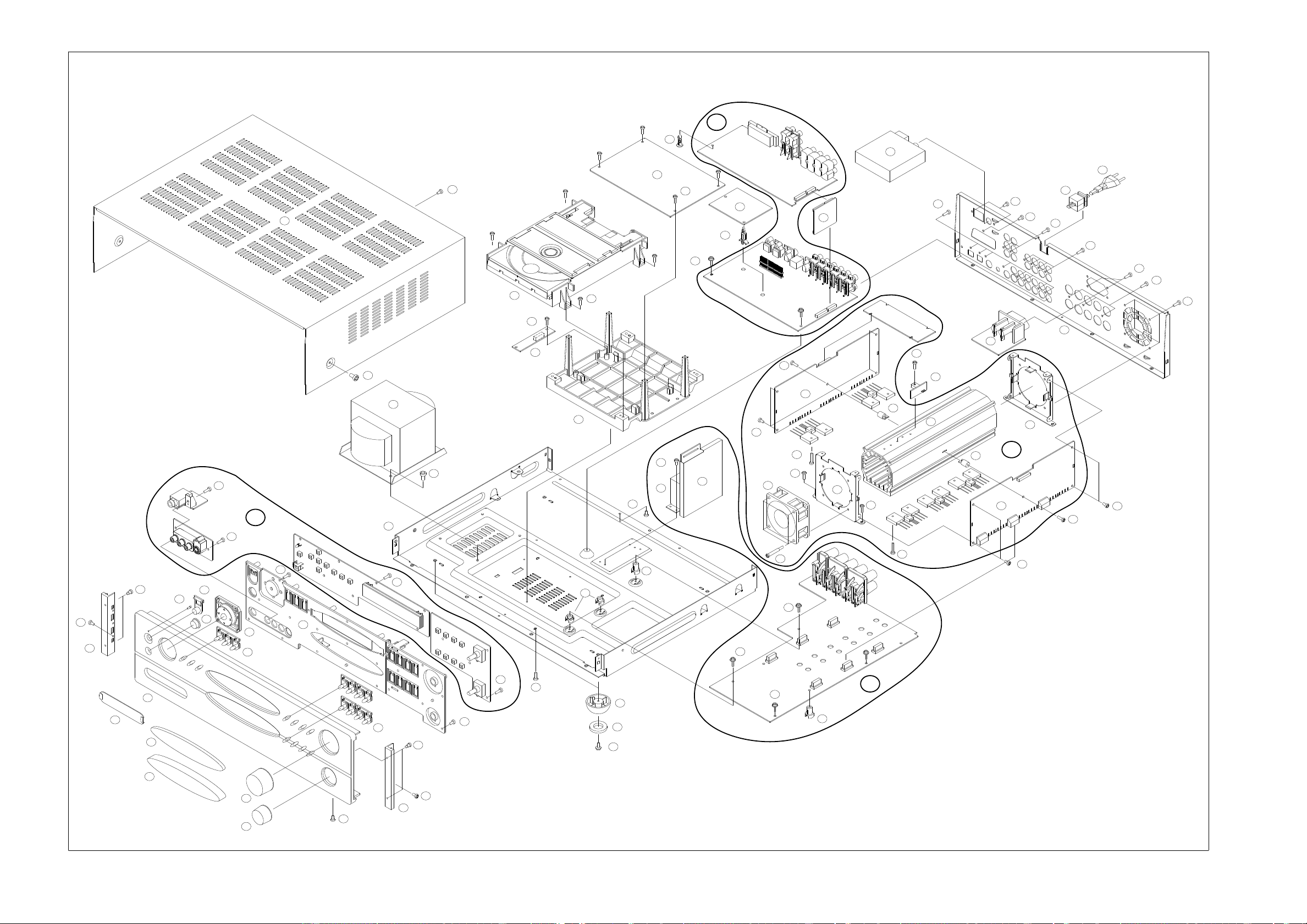
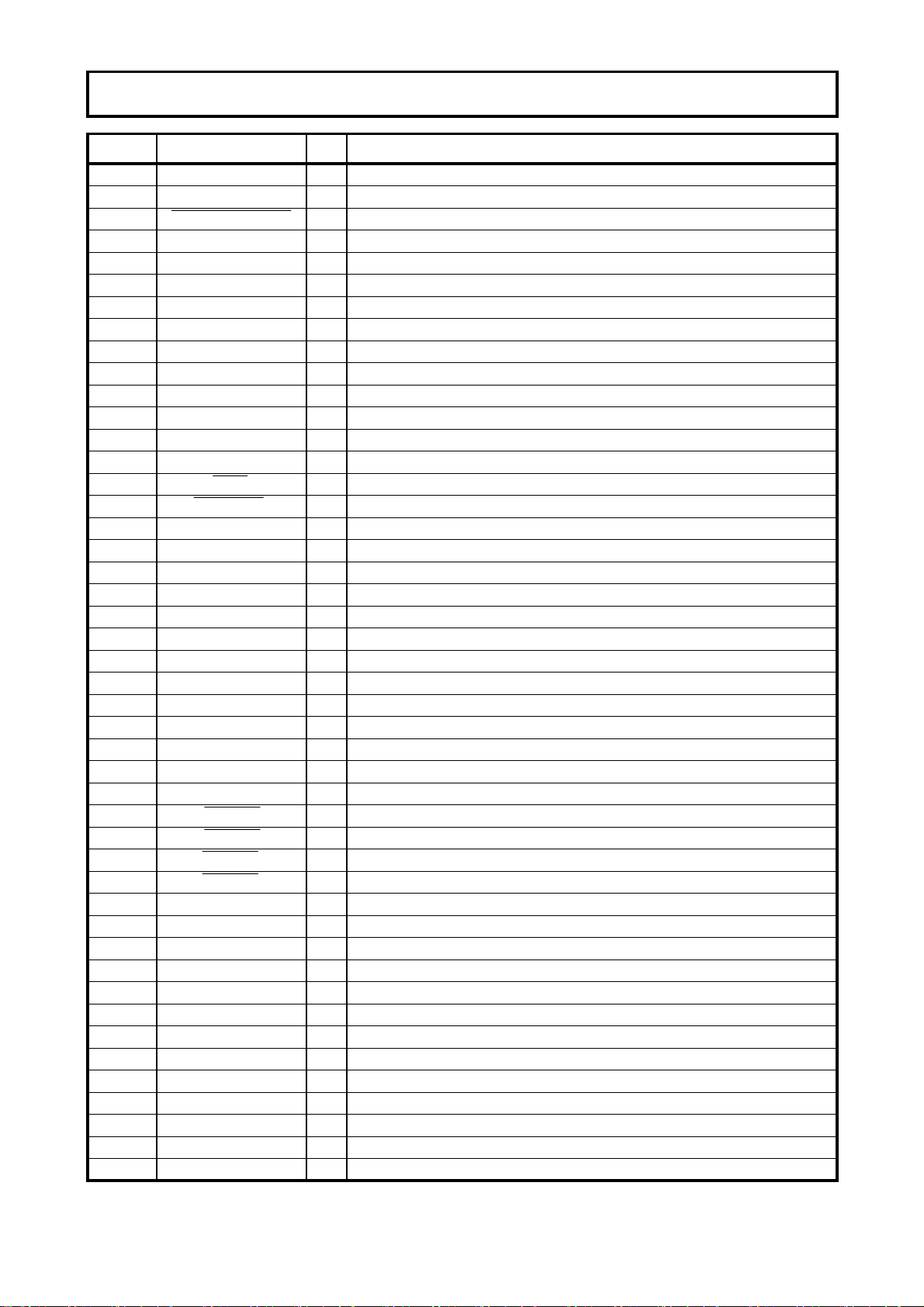
EXPLODED VIEW : L73C
17
34
40
43
33
X6
S4
32
X2
S7
X4
S7
X4
S7
X8
38
S6
13
X2
39
X2
S9
X2
S6
S20
44
X2
S6
36
24
13
X2
S8
S10
S2
13
28
19
30
X4
S1
29
27
26
45
X4
S6
X2
S6
X3
S6
X4
S5
S15
X5
S16
X4
S7
13
18
S2
41
X4
S1
42
25
X6
S12
26
S11
29
31
28
S10
X2
S1
S7
S15
S14
X4
S2
X8
S18
X2
12
11
S1
7
10
9
15
8
S7
23
X4
S7
X4
S7
6
1
2
X4
8
S18
X2
S19
X20
S9
22
S13
S12
S9
X4
20
X4
21
X4
X2
22
24
X9
X2
S1
3
4
S1
7
X4
5
S3
1-9 1-10
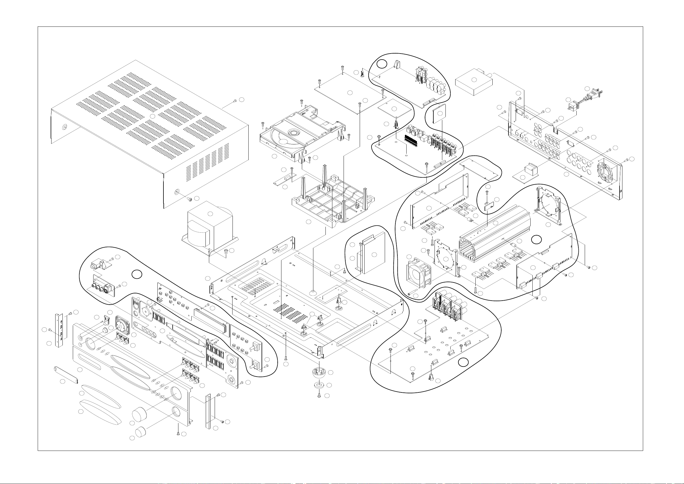
EXPLODED VIEW : L73AH
17
34
40
43
33
X6
S4
32
X2
S7
X4
S7
13
X2
S8
X4
S7
38
X2
39
X2
S9
13
S6
S2
S10
13
S5
44
X8
24
S20
X3
X2
S6
36
28
19
30
X4
S1
29
27
26
45
X4
S6
X2
S6
X3
S6
X4
S5
S15
X5
S16
X4
S7
13
18
S2
41
X4
S1
42
25
X6
S12
26
S11
31
29
28
S10
X2
S1
S7
S15
S14
X4
S2
X8
S18
X2
12
11
S1
7
10
9
15
8
S7
23
X4
S7
X4
S7
6
1
2
X4
8
S18
X2
S19
X20
S9
22
S13
S17
24
S9
X4
20
X4
21
X4
X2
22
X9
X2
S1
3
4
S1
7
X4
5
S3
1-11 1-12
Y
L73AH/C EXPLODED VIEW PARTS LIST
1-13
CJA523FBYA CORD, POWER(AH Ver.) 1
45
CJA2B068ZA CORD, POWER(C Ver.) 1
44 KHR1A028 BUSHING, AC CORD 1
HNVTFCE1U116A TUNER MODULE(AH Ver.) 1
43
CNVKSTMB014MA18 TUNER MODULE(C Ver.) 1
42 CMX1A139 INSULATOR 1
CLT5L055ZU SUB TRANS.ASS'Y(AH Ver.) 1
41
CLT5L055ZE SUB TRANS.ASS'Y(C Ver.) 1
40 KRE1A056 SUPPORT, PCB 1
39 KRE1A058 SUPPORT, PCB 2
38 CIP11755BSMD DSP PCB ASS'Y 1
CKF4A244WK1 PANEL, REAR(AH Ver.) 1
36
CKF3A244VK1 PANEL, REAR(C Ver.) 1
COP11736B
34
COP11736C
COP11737B
33
COP11737C
32 HJDRL-S2004ZA MECHANISM ASS'Y 1
31 CMYL70CCC
30 CMH2A189 SUPPORT, MECHA 1
29 CMH1A119 MOUNT, PCB 2
28 CUP11555Z AMP PCB ASS'Y 1
27 CMY1A197 HEAT SINK 1
26 CMD1A479 BRACKET, HEATSINK 2
25 HDMKD1206PTS3 FAN 1
COP11556D POWER PCB ASS'Y(AH Ver) 1
CTB3+8GFZ SCREW(AH Ver.) 3 COP11556E POWER PCB ASS'Y(C VER)
S20
CHD1A055 SCREW(C Ver.) 1 23 CHE1A030 HOLDER, PCB 2
S19 CTB3+6F SCREW 20 22 CHE170 HOLDER, PCB 2
S18 CHD1A016 SCREW 4 21 CHG1A297 CUSHION, FOOT 4
S17 CTW3+14J SCREW 1 20 CKL1A086 FOOT 4
S16 CHD1A023 SCREW,TRANS. 4 CLT5V031ZU POWER TRANS. (AH Ver.) 1
S15 CHD1A012 SCREW,TR 15 CLT5V031ZE POWER TRANS. (C Ver.) 1
S14 CHD1A036 SCREW,FAN 4 18 CUA1A223 CHASSIS, BOTTOM 1
S13 CTW3+20J SCREW 1 17 CKC1A141S35 CABINET, TOP 1
S12 CTB3+14J SCREW 1 15 CGW1A351M7K102 PANEL, SUB 1
S11 CTB3+20J SCREW 1 13 COP11738B FRONT PCB ASS'Y 1
S10 CTB3+16J SCREW 2 12 CBT1A746M7K102 KNOB, POWER 1
S9 CTW3+8J SCREW 9 11 CGL1A188 INDICATOR, POWER 0.17
S8 CTB4+6FFC SCREW 2 10 CGU1A245A10 WINDOW, SENSOR 1
S7 CTB3+10G SCREW 28 9 CBT1A853M7K102 KNOB, ENTER 1
S6 CTB3+10GFZ
S5 CTB3+8JFZ
S4 CTB3+8JFC SCREW 6 4 HGK2A063YA VOLUME KNOB ASS'Y 1
S3 CTS3+8J SCREW 4 3 CGR1A287M7YK102 ORNAMENT, DOOR 1
S2 CTB3+8J SCREW 7 2 CGU1A244A8 WINDOW, FIP 1
S1 CTB3+6J SCREW 15 1 CGR1A288M7K102 COVER, JACK 1
NO. PARTS NO. DESCRIPTION Q'TY NO. PARTS NO. DESCRIPTION Q'TY
SCREW(AH Ver.) 19 8 CBT1A745M7K102 KNOB, DISPLAY 5
SCREW(C Ver.) 21 7 CKM2A062C37 BAR, SIDE 2
SCREW(AH Ver.) 5 6 CKM1A130XC37 PANEL, AL 1
SCREW(C Ver.) 4 5 HGK1A081ZA ROTARY KNOB ASS'Y 1
24
19
INPUT,DSP & VIDEO
PCB ASS'Y(AH Ver.)
INPUT,DSP & VIDEO
PCB ASS'Y(C Ver.)
MICOM & POWER SUPPLY PCB
ASS'Y(AH Ver.)
MICOM & POWER SUPPLY PCB
ASS'Y(C Ver.)
AMPLIFIER ASS'
1
1
1

2-1
SECTION 2
ELECTRICAL CONTENTS
CONTENTS
IC BLOCK DIAGRAMS & PIN DESCRIPTION .......................................................................................... 2-2
DIAGRAM .................................................................................................................................................... 2-27
1. BLOCK DIAGRAM ................................................................................................................................ 2-27
2. WIRING DIAGRAM .............................................................................................................................. 2-29
3. SCHEMATIC DIAGRAM ...................................................................................................................... 2-31
•
FRONT PART ............................................................................................................................. 2-31
•
µ-COM & POWER SUPPLY PART............................................................................................ 2-33
•
INPUT & VOLUME PART........................................................................................................... 2-35
•
CODEC & LPF PART ................................................................................................................. 2-37
•
DSP PART................................................................................................................................... 2-39
•
VIDEO PART............................................................................................................................... 2-41
•
AMP PART .................................................................................................................................. 2-43
•
POWER PART ............................................................................................................................ 2-45
4. PRINTED CIRCUIT BOARDS ............................................................................................................. 2-47
•
FRONT PART ............................................................................................................................. 2-47
•
µ-COM & POWER SUPPLY PART............................................................................................ 2-49
•
DSP PART................................................................................................................................... 2-50
•
INPUT, VOLUME, CODEC, LPF & VIDEO PART..................................................................... 2-51
•
AMP PART .................................................................................................................................. 2-55
•
POWER PART ............................................................................................................................ 2-57
5. TROUBLESHOOTING .......................................................................................................................... 2-59
2-2
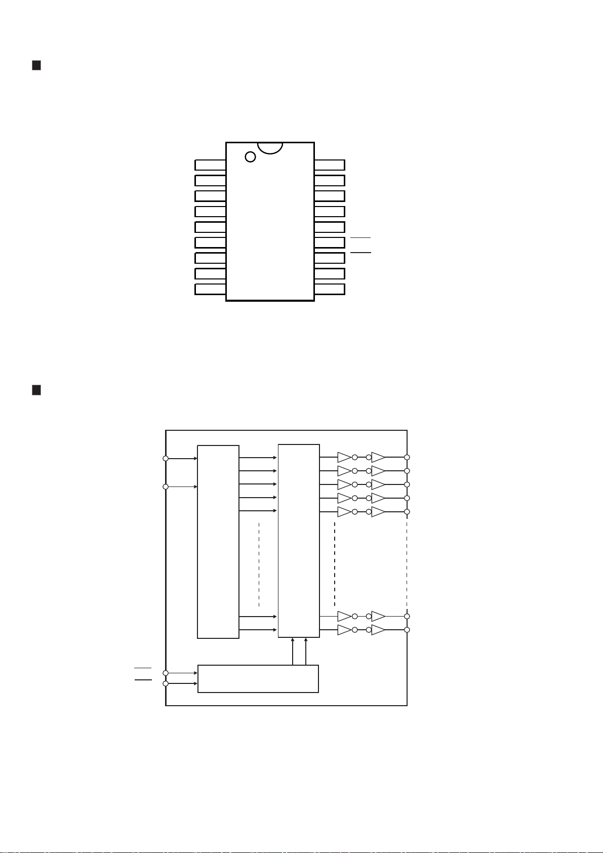
I.C PIN DESCRIPTIONS ( IC81 : FLASH u-COM : ST92F124VIT6 )
PIN No PIN Name I/O
1 T-MUTE O
2 DVD_FAN O
3 N.C
4 N.C
5 SIN I
6 SOUT O
7 TXCLK O
8 RXCLK I
9 VFD_DATA O
10 VFD_CK O
11 VFD_CS O
12
13
14 GND1 15 VDD1 16 V-MUTE O
17 ROM-SEL O
18
19
20
21
22 DVD_RESET O
23 DVD_FREQ O
24 GND 25 DVD_TX O
26 DVD_RX I
27 DVD_CLK I
28 VREG 29 N.C 30 PLL_DOUT I
31 TUNED I
32 N.C 33 PLL_CE O
34 STEREO I
35 PLL/FUNC_DA O
36 PLL/FUNC_CLK O
37 FUNC_CE I
38 GND2 39 VDD2 40 VREG 41 VTEST 42 EVOL_CE O
43 EVOL_DA O
44 EVOL_CK O
45 RDS_DA I
46
47
48 AK_INTERRUPT I
49 AK/CS_CK O
50 AK/CS_DA O
51 DATA_IN I
52
53
N.C
N.C
NC - No Connection
NC No Connection
Function
Tuner mute port
DVD Fan port
No Connection
Micom update port
Micom update port
Micom update TX port
Micom update RX port
VFD Display Data out port
VFD Display Clock port
VFD Display Chip selector port
-
-
-
No Connection
GND Port1
Power Supply Port1
Video mute port
8M Flash Memory (IC46) selector port
No Connection
DVD Reset port
DVD Request port
GND
DVD Data out port (TX)
DVD Data in port (RX)
DVD Chip enable port
Stabilization capacitor(s) for internal voltage regulator
No Connection
PLL Data OUT port
Tuner module TUNED control port
No Connection
PLL Chip enable port
Tuner module STEREO control port
PLL/FUNCTION data output port
PLL/FUNCTION clock output port
FUNCTION IC chip enable port
GND2
Power Supply port2
Stabilization capacitor(s) for internal voltage regulator
Must be kept low in standard operating mode
Electronic volume IC chip enable port
Electronic volume IC data port
Electronic volume IC clock port
RDS data in port
DIR+CODEC (IC31) interrupt port
DSP(IC45) / DIR+CODEC(IC31) clock port
DSP(IC45 )/ DIR+CODEC(IC31) data out port
DSP(IC45) / DIR+CODEC(IC31) data in port
2-3
PIN No PIN Name I/O
54 DSP_RESET I
55 AK_RESET I
56 AK_CE I
57 HINBSY I
58 DSP_C_CS O
59 DSP_AB_CS O
60 INT_REQ I
61 GND3 62 VDD3 63 FINTREQ I
64 REMOTE_IN I
65 HOST_CE I
66 RDS_CLK I
67 DVD_MREQ I
68 OPTION1 I
69 OPTION2 I
70 NC 71 KEY_IN1
72 KEY_IN2
73 KEY_IN3
74 VOL_B
75 VOL_A
76 FUNC_A I
77 FUNC_B I
78 FAN_DET I
79 AVDD 80 GND4 81 POWER_H O
82 FUNC_MUTE(H) O
83 H/PHONE_IN(L) I
84 DVDPW_ON O
85 DVDA_SEL O
86 EXP_CLK O
87 EXP_DA O
88 EXP_CE O
89 GND5 90 VDD4 91 OSCIN 92 OSCOUT 93 RESET I
94 HW0SW1 95 N.C 96 PROTECT_IN(L) I
97
98
99 RTC_SDA O
100 RTC_SCL O
N.C -
Function
DSP(IC45) reset port
DIR+CODEC(IC31) reset port
DIR+CODEC(IC31) chip enable port
HOST BUSY
DSP(IC45) C Chip selector port
DSP(IC45) AB Chip selector port
DSP(IC45) interrupt request port
GND3
Power Supply port3
DSP(IC45) interrupt request port
System remote Input port
HOST(IC81) Chip enable port
RDS Clock port
DVD Main request port
* H : FM 50KHz step ,* L : FM 100KHz step
* H : AM 9KHz step ,* L : AM 10KHz step
No Connection
I
I
KEY Data input port
Volume Data Input port(Master Volume)
Function A control port
Function B control port
Fan Detector port
Analog Power Supply port
GND4
Power on control port (Active "H")
Function mute port (Active "H")
Headphone in port (Active "L")
DVD Power ON port
DVD Audio selector port
Expander IC14 Clock port
Expander IC14 Data out port
Expander IC14 Chip enable port
GND5
Power Supply port4
4MHz Crystal Connection port
Reset port
Watchdog option port
No Connection
Protection port (Active"L")
No Connection
Real time control serial data out port
Real time control serial clock port
2-4
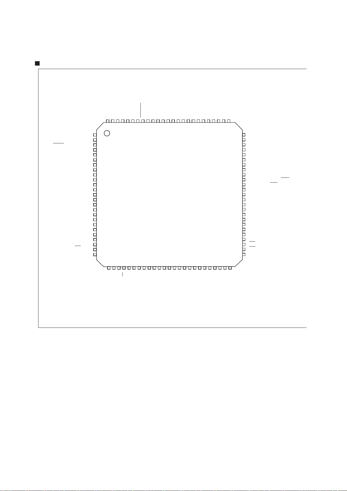
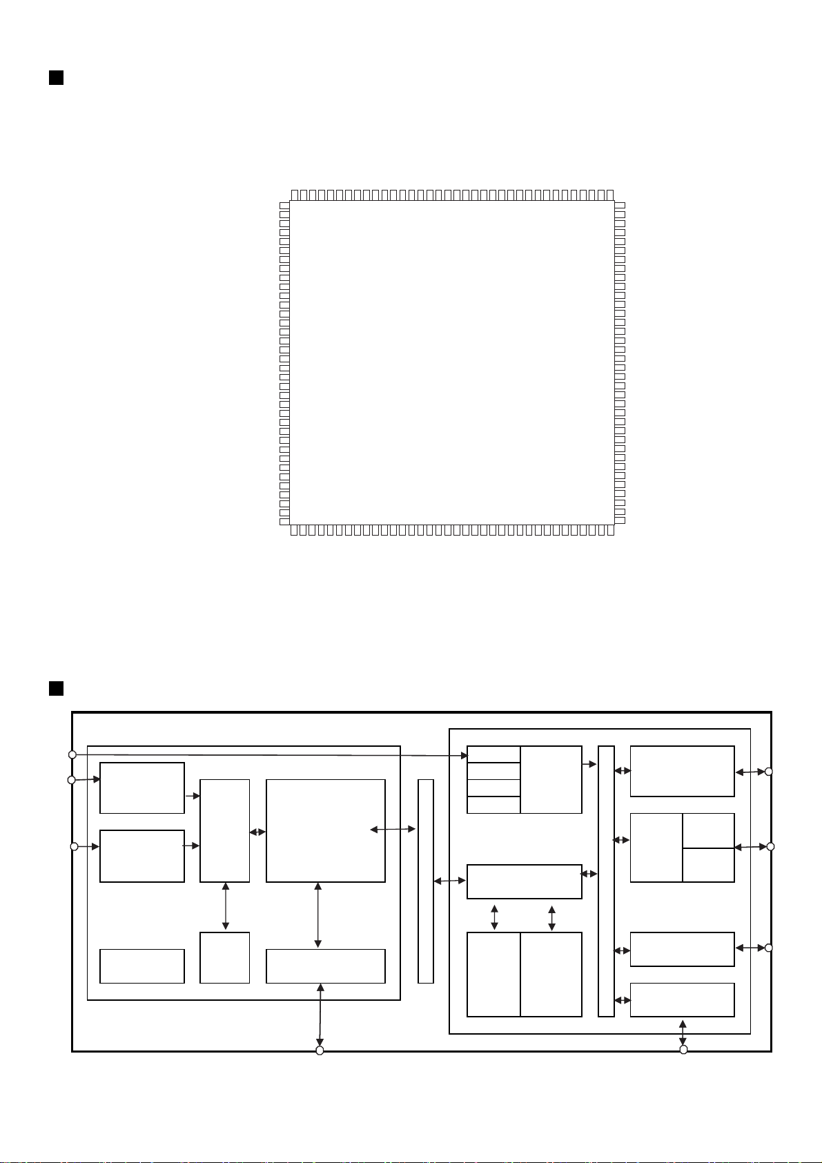
ST92F124V1: Pin Configuration (Top-view TQFP100)
SS
RESET
OSCOUT
DD
P7.7/AIN15/7/ WKUP13
P7.6/AIN14/WKUP12
OSCIN
V
P7.5/AIN13/WKUP11
V
A20/P9.6
A21/P9.7
W
AIT/WKUP5/P5.0
WKUP6/WDOUT/P5.1
SIN/WKUP2/P5.2
WDIN/SOUT/P5.3
TXCLK/CLKOUT/P5.4
RXCLK/WKUP7/P5.5
DCD/WKUP8/P5.6
WKUP9/RTS/P5.7
ICAPA1/P4.0
CLOCK2/P4.1
OCMPA1/P4.2
V
V
ICAPB1/OCMPB1/P4.3
DD
EXTCLK1/WKUP4/P4.4
EXTRG/STOUT/P4.5
SDA/P4.6
WKUP1/SCL/P4.7
ICAPB0/P3.1
ICAPA0/OCMPA0/P3.2
OCMPB0/P3.3
EXTCLK0/SS
/P3.4
MISO/P3.5
P9.5/A19
P9.4/A18
P9.2/A16
P9.3/A17
100999897969594939291908988878685848382818079787776
1
2
3
4
5
6
7
8
9
10
11
12
13
14
SS
15
16
17
18
19
20
21
22
23
24
25
27 28 29 30 31 32 33 34 35 36 37 38 39 40 41 42 43 44 45 4647 48 49 50
26
HW0SW1
P9.0/RDI
P9.1/TDO
ST92F124V1
P7.4/AIN12/WKUP3
P7.1/AIN9
P7.3/AIN11
P7.0/AIN8/CK_AF
P7.2/AIN10
P8.7/AIN7
AVSSAVDDP8.6/AIN6
P8.5/AIN5
75
P8.4/AIN4
74
P8.3/AIN3
73
P8.2/AIN2
72
P8.1/AIN1/WKUP15
71
P8.0/AIN0/WKUP14
70
NC
69
P6.5/WKUP10/INTCLK
68
P6.4/NMI
67
P6.3/INT3/INT5
66
P6.2/INT2/INT4/DS2
65
P6.1/INT6/RW
64
P6.0/INT0/INT1/CLOCK2/8
63
P0.7/A7/D7
V
62
DD
V
61
SS
P0.6/A6/D6
60
P0.5/A5/D5
59
P0.4/A4/D4
58
P0.3/A3/D3
57
P0.2/A2/D2
56
P0.1/A1/D1
55
P0.0/A0/D0
54
AS
53
DS
52
P1.7/A15
51
RW
REG
V
MOSI/P3.6
SCK/WKUP0/P3.7
* V
must be kept low in standard operating mode.
TEST
SS
DD
V
V
TEST
REG
V
*V
A8/P1.0
A9/P1.1
TINPB0/P2.1
TINPA0/P2.0
TINPB1/P2.5
TINPA1/P2.4
TOUTA0/P2.2
TOUTB0/P2.3
TOUTB1/P2.7
TOUTA1/P2.6
NC
WKUP6
A10/P1.2
A11/P1.3
A12/P1.4
A13/P1.5
A14/P1.6
2-5
ST92F124V1: Architectural Block Diagram
RW
WAIT
NMI
DS2
RW
INT[6:0]
WKUP[15:0]
OSCIN
OSCOUT
RESET
CLOCK2/8
INTCLK
CK_AF
STOUT
ICAPA0
OCMPA0
ICAPB0
OCMPB0
EXTCLK0
ICAPA1
OCMPA1
ICAPB1
OCMPB1
EXTCLK1
TINPA0
TOUTA0
TINPB0
TOUTB0
TINPA1
TOUTA1
TINPB1
TOUTB1
V
REG
AS
DS
FLASH
128 Kbytes
3 TM
E
1 Kbyte
RAM
4 Kbytes
256 bytes
Register File
8/16 bits
CPU
Interrupt
Management
ST9 CORE
RCCU
ST. TIMER
EF TIMER 0
EF TIMER 1
MF TIMER 0
MF TIMER 1
VOLTAGE
REGULATOR
Ext. MEM.
ADDRESS
DATA
Port0
Ext. MEM.
ADDRESS
Ports
1,9
A[7:0]
D[7:0]
A[10:8]
A[21:11]
P0[7:0]
P1[7:3]
Fully
MEMORY BUS
Prog.
I/Os
P1[2:0]
P2[7:0]
P3[7:4]
P3[3:1]
P4[7:4]
P4[3:0]
P5[7:0]
P6[5:2,0]
P6.1
P7[7:0]
P8[7:0]
P9[7:0]
I2C BUS
WATCHDOG
SDA
SCL
WDOUT
HW0SW1
MISO
SPI
REGISTER BUS
ADC
MOSI
SCK
SS
AV
DD
AV
SS
AIN[15:8]
AIN[7:0]
EXTRG
TXCLK
RXCLK
SIN
SCI M
DCD
SOUT
CLKOUT
RTS
SCI A
RDI
TDO
The alternate functions (
Port8 and Port9.
Italic characters
) are mapped on Port 0, Port 1, Port2, Port3, Port4, Port5, Port6, Port7,
2-6
I.C PIN DESCRIPTIONS (IC45 : AUDIO DSP : CS494003)
PIN No PIN Name I/O
1 UHS0 O
2 HUS1 O
3 INTREQ,ABODY O
4 FA1,FSCDIN I
5 GPIO20 O
6 FA0,FSCCLK I
7 FHS2,FSCDIO O
8 GPIO21 O
9 FDAT7 I
10 VDD6
11 VSS6
12 FWR,FDS I
13 FRD,FR/W O
14 FDAT6 I
15 FCS I
16 FINTREQ O
17 FDBCK I
18 FDAT5 I
19 FDAT4 I
20 VDD7
21 VSS7
22 FDAT3 I
23 FDBDA I
24 FDAT2 I
25 DBDA I
26 DBCK I
27 FDAT1 I
28 TEST I
29 FDAT0 I
30 NV_WE O
31 NV_OE O
32 NV_CS O
33 SD_WE O
34 SD_DATA0 O
35 SD_DATA1 O
36 SD_DATA2 O
37 SD_DATA3 O
38 SD_DATA4 O
39 SD_DQM0 O
40 SD_DATA5 O
41 VSSSD4
42 VDDSD4
43 SD_DATA6 O
44 SD_DATA7 O
45 SD_DQM1 O
46 SD_DATA15 O
Function
DSP C Control Mode Select BIT 0
DSP C Control Mode Select BIT 0
Open-drain interrupt-request output
Host Address Bit One or SPI Serial Control data input
General Purpose output
Host parallel Address Bit Zero or Serial Control Port Clock
DSP AB Control port mode select bit2
General Purpose output
DSP AB Bidirectional data bus
2.5V Supply Voltage
2.5V Ground
Host write Strobe or Host data strobe
Host Parallel Output Enable or
DSP AB Bidirectional data bus
Host Parallel Chip Select , Host Serial SPI Chip Select
Open-drain interrupt-request output
Reserved
DSP AB Bidirectional data bus
DSP AB Bidirectional data bus
2.5V Supply Voltage
2.5V Ground
DSP AB Bidirectional data bus
Reserved
DSP AB Bidirectional data bus
Debug Data
Debug Clock
DSP AB Bidirectional data bus
Reserved
DSP AB Bidirectional data bus
SRAM Write Enable
SRAM Output Enable
SRAM Chip Select
SDRAM Write Enable
SDRAM Data Bus 0
SDRAM Data Bus 1
SDRAM Data Bus 2
SDRAM Data Bus 3
SDRAM Data Bus 4
SDRAM Data Mask 0
SDRAM Data Bus 5
SDRAM Ground
SDRAM Power Supply
SDRAM Data Bus 6
SDRAM Data Bus 7
SDRAM Data Mask 1
SDRAM Data Bus 15
2-7
PIN No PIN Name I/O
47 SD_DATA14 O
48 NC5
49 SD_DATA13 O
50 VSSSD3
51 VDDSD3
52 SD_DATA12 O
53 SD_DATA11 O
54 SD_DATA10 O
55 SD_DATA9 O
56 SD_DATA8 O
57 VSSSD2
58 VDDSD2
59 SD_CLK_OUT O
60 SD_ADR9 O
61 SD_CLK_IN I
62 SD_ADR8 O
63 SD_ADR7 O
64 SD_CLK_EN I
65 SD_ADR6 O
66 SD_ADR5 O
67 SD_ADR4 O
68 SD_CS I
69 VSSSD1
70 VDDSD1
71 SD_BA O
72 SD_ADR10 O
73 SD_ADR0 O
74 SD_ADR1 O
75 SD_ADR2 O
76 SD_ADR3 O
77 SD_RAS O
78 SD_CAS O
79 SDATAN3 I
80 SDATAN2 I
81 SDATAN1 I
82 SDATAN0 I
83 NC4
84 NC3
85 LRCLKN I
86 SCLKN I
87 LRCLK1 O
88 NC2
89 NC1
90 VDD1
91 VSS1
92 XMT958,AUDATA7 O
93 AUDATA6 O
94 AUDATA5 O
95 HDATA7 O
Function
SDRAM Data Bus 14
No Connect (Ground)
SDRAM Data Bus 13
SDRAM Ground
SDRAM Power Supply
SDRAM Data Bus 12
SDRAM Data Bus 11
SDRAM Data Bus 10
SDRAM Data Bus 9
SDRAM Data Bus 8
SDRAM Ground
SDRAM Power Supply
SDRAM CLOCK DATA OUT
SDRAM Address Bus
SDRAM CLOCK DATA IN
SDRAM Address Bus 8
SDRAM Address Bus 7
SDRAM Ground
SDRAM Address Bus 6
SDRAM Address Bus 5
SDRAM Address Bus 4
SDRAM Chip Select
SDRAM Ground
SDRAM Power Supply
SDRAM Bank Address Select
SDRAM Address Bus 10
SDRAM Address Bus 0
SDRAM Address Bus 1
SDRAM Address Bus 2
SDRAM Address Bus 3
SDRAM Row Address Strobe
SDRAM Column Address Strobe
PCM Audio input Data 3
PCM Audio input Data 2
PCM Audio input Data 1
PCM Audio input Data 0
No Connect (Ground)
PCM audio input sample rate clock
PCM audio input bit clock
Audio Output Sample Rate Clock
No Connect (Ground)
2.5V Supply Voltage
2.5V Ground
Digital Audio Output 7 , S/PDIF Transmitter
Digital Audio Output 6
Digital Audio Output 5
DSP C Bidirectional data bus 7
2-8
PIN No PIN Name I/O
96 HDATA6 O
97 HDATA5 O
98 SCLK1 O
99 MCLK I
100 VDD2
101 VSS2
102 AUDATA4 O
103 HDATA4 O
104 SCLK0 O
105 HDATA3 O
106 AUDATA3 O
107 AUDATA2 O
108 LRCLK0 O
109 AUDATA1 O
110 AUDATA0 O
111 CMPCLK,SCLKN2 I
112 HDATA2 O
113 VSS3
114 VDD3
115 HDATA1 O
116 HDATA0 O
117 CMPREQ,FLRCLK2 I
118 CMPDAT,FSDATA2 I
119 FLRCLKN1 I
120 WR,DS I
121 RD,R/W I
122 PLLVSS
123 FILT2
124 FILT1
125 PLLVDD
126 XTALO O
127 XTAL,1CLKIN I
128 CLKSEL I
129 CS O
130 A0 O
131 FSDATAN1 I
132 VDD4
133 VSS4
134 FSCLKN1,STCLK2 I
135 SCS I
136 SCDIN I
137 VSS5
138 VDD5
139 A1 O
140 SCDOUT O
141 HNBSY I
142 SCCLK O
143 UHS2,CS_OUT O
144 RESET I
Function
DSP C Bidirectional data bus 6
DSP C Bidirectional data bus 5
Audio output bit clock
Audio Master clock
2.5V Supply Voltage
2.5V Ground
Digital Audio Output 4
DSP C Bidirectional data bus 4
Audio output bit clock
DSP C Bidirectional data bus 3
Digital Audio Output 3
Digital Audio Output 2
Audio Output Sample Rate Clock
Digital Audio Output 1
Digital Audio Output 0
PCM audio input bit clock
DSP C Bidirectional data bus 2
2.5V Ground
2.5V Supply Voltage
DSP C Bidirectional data bus 1
DSP C Bidirectional data bus 0
PCM Audio Data input bit clock
PCM Audio data input Number two
PCM audio data input one
DSP AB Control port mode select bit 0
DSP AB Control port mode select bit 1
PLL Ground voltage
Phase-Locked Loop Filter
Phase-Locked Loop Filter
PLL supply voltage
Crystal OSC Output
External Clock input/Crystal OSC input
DSP Clock select
Host parallel Chip Select
Host Parallel Address bit 0
PCM Audio Data input one
2.5V Supply Voltage
2.5V Ground
PCM audio input bit clock
Host Serial SPI Chip Select (Active "L")
SPI Serial control data input
2.5V Ground
2.5V Supply Voltage
Host Address bit 1
Serial control port data
Input Host Message status
Serial control port clock
DSP C Control Mode Select BIT 2
Master Reset Input
2-9
y
PIN ASSIGNMENT(IC45: CS494003)
A
859
3
TMX
O
IP
,3ATAD
G
2
,
0
3
A
0
T
K
A
A
L
TADH
K
L
D
CR
CS
UA
UA
L
1
8
9
1
1
OI
O
I
PG
P
G
,
,0
1S
S
H
H
U
U
501
5
02
TO
NID
OIPG
OB
C
S
A
F
,1AF
QE
R
T
NI,
AUDATA1
AUDATA0
CMPCLK, FSCLKN2
HDATA2, GPIO2
VSS3
VDD3
HDATA1, GPIO1
HDATA0, GPIO0
CMPREQ, FLRCLKN2
CMPDAT, FSDATAN2
FLRCLKN1
WR, DS, GPIO10
RD, R/W, GPIO11
PLLVSS
PLLVDD
CS, GPIO9
A0, GPIO13
FSDATAN1
VDD4
FSCLKN1, STCCLK2
UHS2, CS_OUT, GPIO17
VSS4
SCS
SCDIN
VSS5
VDD5
A1, GPIO12
SCDOUT, SCDIO
HINBSY, GPIO8
SCCLK
RESET
110
115
120
125
130
135
140
144
13
OI
P
G
,
B85
0
8
2
4
OI
OI
PG
P
,4
G ,4A
A
T
K
2
AD
2S
T
L
A
D
C
D
SV
D
U
A
M
H
V
00
1
9
3
2
5
OIP
G
,5
1
A
T
K
A
L
DH
CS
9TMX
6OI
7O
O
OI
I
I
P
P
P
P
G
G
,
,
,6
G ,6A
G
5
7
,
7
A
AT
A
T
T
ATAD
T
A
D
H
H
5
9
1
ADUA
A
A
1S
D
D
D
S
D
U
U
A
A
V
V
09
3
2OIP
22
O
IP
G
,
G ,NK
NK
1
K
LC
L
2C
1
L
C
C
C
R
R
N
L
S
N
L
58
CS494003
0
1
7T
1
6
T
KLC
2
DD
U
A
OI
ODC
D
V
CS
P
F
G
F
S
,
F
,OI
OAF
D
C
S
F
,
2
S
HF
6
S
S
V
S
/
D
RF
F
,
,W
R
D
W
R
F
F
,
,1
0SH
SHF
F
51
6
S
TADF
C
F
02
7
7
5
4
KCB
Q
T
TA
E
AD
RT
D
D
F
F
F
NI
F
2T
3
A
T
SS
DDV
D
AD
AD
B
V
D
F
F
F
5
7
6
2
2
2
2
O
O
O
OI
I
I
I
P
P
P
P
G ,0
G ,
G ,3
G ,
1
2
S
N
A
T
3
4C
A
C
D
S4
N
N
5
2
1
A
K
T
D
CBD
AD
BD
F
S
N
N
N
AC
A
AT
ATA
A
R
T
_
_D
A
AD
D
D
DS
S
S
S
S
08
0
3
6
0T
51
4
T
1
1
SE
A
O
O
O
I
I
I
D
T
P
PG ,
PG ,
F
G
,
SC
E
E
O
W
_
_V
_
V
V
N
N
N
1
2
3
0
A
A
A
A
T
T
T
TX
XE,
XE
XE,
E
,
,
2
3R
0
1
RD
R
R
D
DDA
DD
D
DA
A
A
_D
_D
_
_D
D
S
S
S
S
5
7
SD_ADDR10, EXTA10
SD_BA, EXTA19
VDDSD1
70
VSSSD1
SD_CS
SD_ADDR4, EXTA4
SD_ADDR5, EXTA5
65
SD_ADDR6, EXTA6
SD_CLK_EN
SD_ADDR7, EXTA7
SD_ADDR8, EXTA8
SD_CLK_IN
60
SD_ADDR9, EXTA9
SD_CLK_OUT
VDDSD2
VSSSD2
SD_DATA8, EXTA11
SD_DATA9, EXTA12
55
SD_DATA10, EXTA13
SD_DATA11, EXTA14
SD_DATA12, EXTA15
VDDSD3
50
VSSSD3
SD_DATA13, EXTA16
NC5
SD_DATA14, EXTA17
SD_DATA15, EXTA18
45
SD_DQM1
SD_DATA7, EXTD7
SD_DATA6, EXTD6
VDDSD4
VSSSD4
40
SD_DATA5, EXTD5
SD_DQM0
SD_DATA4, EXTD4
SD_DATA3, EXTD3
5
3
2D
0D
1
E
D
W_
T
TX
TX
XE
DS
E ,
E ,
,2
1AT
0
A
AT
T
A
AD
A
D
D
_
_D
_D
D
S
S
S
BLOCK DIAGRAM(IC45: CS494003)
SAI 0 Serial
Compressed SAI 1 Audio
Digital
Interface SAI 3
Farme
Digital Shifter
Multi-Standard
Audio Decoder
Audio Audio
Input
DSP AB
Input
PLL Clock Buffer
Manager RAM
Parallel or Serial
Host Interface
S
H
A
R
E
D
M
E
M
O
R
Y
SAI 2 Interface
DSP C
Programmable
32-Bit DSP
DSP DSP
RAM ROM
External Memor
Interface
I
N
T
Digital
E
R
Output
N
A
L
B
GPIO and I/O
U
S
Controller
Parallel or Serial
Host Interface
DAO 0
DAO 1
2-10
NJU3713
(IC14 : EXPANDER / MAIN)
BLOCK DIAGRAM
DATA
CLK
P5
P6
P7
P8
Vss
P9
P10
P11
P12
10
11
1
2
3
4
5
6
7
8
9
18
17
16
15
14
13
12
11
10
DD
V
P4
P3
P2
P1
CLR
STB
CLK
DATA
14
15
16
17
P1
P2
P3
P4
1
P5
STB
CLR
12
13
Shift Circuit
Controller Circuit
Latch Circuit
8
P11
9
P12
2-11
A
X
I.C PIN DESCRIPTIONS (IC31:AUDIO CODEC WITH DIR : AK4588)
PIN No PIN Name I/O
1 AK_INT O
2NC
3 TVDD
4 DVDD
5 DVSS
6NC
7 XTAL_IN I
8 DVSS
9 MCLK O
10 MCLK O
11 NC
12 NC
13 NC
14 SDATA1 O
15 FSCLK O
16 FLRCLK O
17 SDATA2 O
18 SCLK0 O
19 LRCLK1 O
20 AK/CS_DOUT O
21 AK/CS_CK I
22 AK/CS_DA I
23 AK_CE I
24 GND
25
26 AUDIODATA2 I
27 AUDIODATA1 I
28 AUDIODATA0 I
29 GND
30 +5VD
31 AK_RST
32 DVSS
33 NC
34 NC
35 DMIXL_DSP O
36 NC
37 DMIXR_DSP O
38 NC
39 SR-DSP O
40 NC
41 SW-DSP O
UDIODATA_DMI
I
Function
Interrupt pin
Not connect
3.3V Power Supply
5V Power Supply
Digital ground pin
Not connect
X`tal clock input pin
Digital ground pin
Masster clock
Masster clock
Not connect
Not connect
Not connect
Audio serial data 1
Systm clock
Audio serial data L/R clock
Audio serial data 2
Bit clock
Audio serial data L/R clock
Digital audio out
System clock
Control data
Chip enable
High impeadance ground
Audio data downmix data
AUDIODATA2
AUDIODATA1
AUDIODATA0
High impeadance ground
5V Pull up
Chip reset
Digital ground pin
Not connect
Not connect
Downed L-ch analog output
Not connect
Downed R-ch analog output
Not connect
Surround right-ch analog output
Not connect
Subwoofer-ch analog output
2-12
PIN No PIN Name I/O
42 NC
43 FR-DSP O
44 NC
45 SL-DSP O
46 NC
47 FL-DSP O
48 NC
49 CEN-DSP O
50 NC
51 ADLIN-DSP I
52 ADRIN-DSP I
53 VCOM
54 +5VD
55 +5VD
56 AVSS
57 SPDIF_IN
58 DVSS
59 OPTICAL_IN
60 DVSS
61 COAXIAL_IN
62 DVSS
63 NC
64 DVSS
65 GND
66 +5VD
67 NC
68 DVSS
69 NC
70 +5VD
71 NC
72 DVSS
73 NC
74 DVSS
75 DAUX2
76 +5VD
77 MCLK
78 NC
79 DIGITAL_OUT
80 AK_INT
Function
Not connect
Front right-ch analog output
Not connect
Surround left-ch analog output
No Connection
Front left-ch analog output
Not connect
Center-ch analog output
Not connect
L-ch analog input
R-ch analog input
GND(AC)
5V power supply port
5V power supply port
Analog ground
SPDIF input port
Digital ground pin
Optical input port
Digital ground pin
Coaxial input port
Digital ground pin
Not connect
Digital ground pin
High impeadance ground
5V power supply port
Not connect
Digital ground pin
Not connect
5V Pull up
Not connect
Digital ground pin
Not connect
Digital ground pin
Auxiliary audio data input port
5V Pull up
Master clock
Not connect
Digital output port
Interrupt pin
 Loading...