

Motorola V66, V66i Service Manual

V66 Family
Standard / Refresh
Level III
Circuit Description
V66 – Level III Circuit Description
2
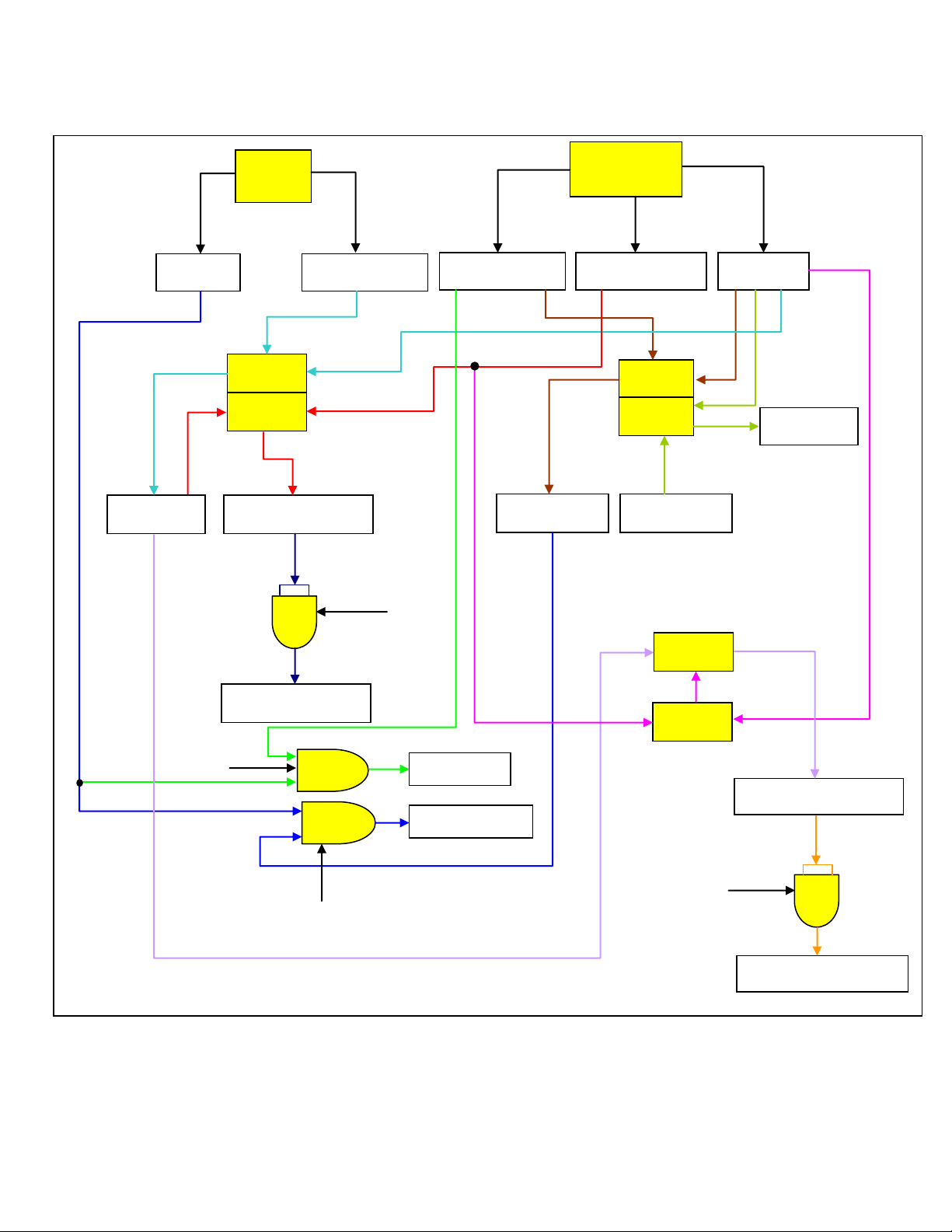
DUMB_SEL2
PIN 10
DUMB_SEL1
PIN 11
DUMB_SEL 3
PIN 12
DUMB
DEVICE
NUMBER
ACCESSORY
0 0 0
0
TTY DEVICE
0 0 1 1 DESKTOP SPEAKERPHONE
0 1 0 2 PTT HEADSET
0 1 1 3 FM RADIO HEADSET
1 0 0 4 IrDA ADAPTOR
1 0 1 5 CLIP ON SPEAKERPHONE
1 1 0 6 SMART AUDIO DEVICE (2)
1 1 1
7 (1)
EASY INSTALL HANDS FREE KIT
(EIHF)
Power
1. Power for the unit can be obtained from 2 sources, the first being taken from the
battery pack of which there will be 2 capaciaty variants, each in the same colour
housing as the phone with which it is sold.
2. The 2 variants will be a Li-Ion 500mAh and an extended life 1100Li-Ion mAh
battery packs
3. The battery block J851 on the PCB will have 4 contacts, these being:
Pin 1 – BATT+ (Description will follow, see point 4)
Pin 2 – BATT_SER_DATA - This feature is used to communicate via the
One-Wire Bus interface with the serial EPROM inside a “Smart” battery.
Charging characteristics supplied by the battery can be read from this line, one
bit at a time. It is supported by V2 and is fed to the Patriot IC – U700 on Pin
G2
Pin 3 –THERM – Senses Battery temperatures for rapid charging, uses AD4
an 8-bit A/D input of GCAP III on Pin M5 to evaluate the voltage and convert
it to and digital value. The potential divider network R925, R928, supports the
THERM line and R947, with the originating voltage provided by
THERMBIAS from GCAP III Pin K6 A internal PMOS pull up that provides
a bias to the external battery thermistor when standby pin is low. –Vd <
V
thermbias
In the case of Sapphire SIMPD1 and SIMPD2 are not used instead
SIMPD0_PB18 is utilized from Patriot.
Pin 4 – Ground
4. BATT+, which should be between V
Battery Select FET Q942 where the incoming battery voltage will be applied to
the multi pin source on Pins 1, 5 & 8.
5. The signal Main originates From GCAP pin P6 called MAIN_FET signal, is
applied to the gate when no Ext B+ is available and allows current flow of
BATT+ from source to drain and then this will be output as B+.
6. The other source of power is from EXT BATT+, for this we use an External
charger, car kit or Vehicle Power Adaptor, the type of power source will be
decided by the inputs on the External connector J850. See below table:
> V2+Vd
– 4.2 V
max
– 2.85V, and is then fed to
min
GSM Service Support
Motorola Proprietary Information

V66 – Level III Circuit Description
3
7. The EXT BATT+ Voltage, which can be anything between V
V
– 3.3V, is then fed from J850 as EXT BATT+ to U901 which acts as a Over
min
– 6.6V
max
Voltage IC This then allows a bias voltage onto the gate of Q945 Pin 4 which
throughputs EXT BATT+ to EXT B+.
8. Ext B+ is sensed by MOBPORTB (Pin K7) GCAP III, this allows sensing of
power supply availability to GCAP III.
9. EXT B+ is then fed through Protection Diode CR940, through S1 of Q945,
passed through to the Drain and out as B+, Biasing provided by Q944. Midrate_1
is pulled low all the times. When charger is connected and phone is turned on then
Midrate_1 momentary goes to 2.14V and then goes back to 0V. This puts the
phone in Charging Battery mode.
10. B+ is then input to GCAP III on Pins J10, J14 and P7. B+ will also then be used
to provide power for the regulators as follows.
11. As power is applied to GCAP III the 32Khz crystal Y900 will start to oscillate
giving the clock signal GCAP_CLK Pin C7 to Patriot Pin L3.
12. The 32Khz clock will then be multiplied by 8 and given to the reference clock
256Khz of the V_BUCK internal reference-switching units. V_ Boost is used to
generate VSIM1 for SIM Card in Sapphire.
13. At this point GCAP III will use B+ and GCAP_CLK to generate V_BUCK. The
BUCK regulator circuit uses a Switch Mode Power Supply Circuit; see below
explanation to generate the correct voltage. The LX1 signal decides the duty cycle
of the output and therefore the amplitude of the voltage.
14. V_BOOST is responsible for voltages above the battery voltage and V_BUCK
below the battery voltage; they are hardwired during manufacturing and will set
up the reference voltages for output. For V66:
PGM0 (Pin J2) = Ground This Gives the following:
PGM1 (PinJ4) = B+ Ref 1 – 2.775V – Pin H12
PGM2 (Pin K2) = Ground Ref 2 – 2.775V – Pin B9
Ref 3 – 2.775V – Pin B11
V1 – 1.875V – Pin E14
V2 – 2.775V – Pin P1
V3 – 1.875V – Pin H14
VSIM1 – 3.00V – Pin M13
15. For V_BUCK, B+ is applied to the PSRC1 input of GCAP III Pin M9, this is fed
into the switching circuit and after the duty cycle is adjusted, the controlled signal
will be fed out as LX1 Pin P9 and the resultant voltage will then be applied to the
appropriate voltage regulators. V1 Pin E13 and V3 Pin G12
16. Inputs to regulators V2 Pin N2 and REF 1 Radio B+ is the inputs to regulators
V2 Pin N2 and REF 1. (Radio B+ is generated by both supply through Q945, and
Q942) are powered by Ext B+ or BATT +
17. VSIM 1 is controlled by V_BOOST which boosts the B+ voltage Pin 3 up to 5V,
output on Pin 1, using a SW mode Power Supply. GCAP_CLK Pin 6 controls
timing for voltage generation The 5V is then fed into GCAP III on Pin M2, where
it will feed the VSIM1 regulator to give 5V to the SIM card should it be required.
GSM Service Support
Motorola Proprietary Information
V66 – Level III Circuit Description
4
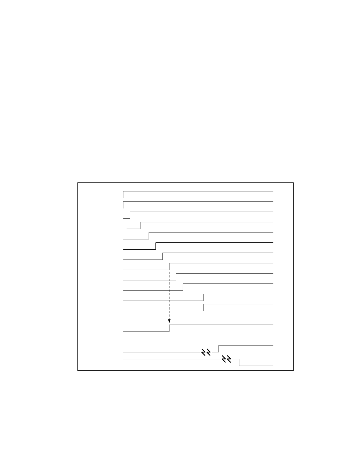
B+
biasen
pll_en
pwm_en
4 mS
10 mS
ref1_en 15 mS
ref2_en 17 mS
ref3_en 19 mS
v2_en 23 mS
v1_en 25 mS
v4_en 31 mS
vsim1_en 31 mS
v3_en 21 mS
v3_ready 21 mS
ST_timer 28 mS
RESETB 78 mS
WDOG 128 mS
PA B+_en
18. At this point the MAGIC DM will then begin to power up.
19. B+ is fed into the Source 1 and 2 of Q201 (Pins 5 & 2 respectively), the Voltage
form GCAP III, VREF provides the bias for Q201 and allows the production of
RF_V1 and RF_V2 from B+. These are output from Q201 on Pins 6 & 4
respectively.
20. RF_V2 and RF_V2 then provide all power requirements to the MAGIC DM,
RF_V1 Input on Pins H7, C8
RF_V2 Input on Pins D8, C6, B3
21. On Power being applied to MAGIC DM there are 2 different reference clocks
produced. Initially, as soon as power is applied to the 26Mhz crystal Y200 will
begin to oscillate driven by XTAL_BASE Pin F2. This will internally be divided
by 2, to give our external system 13MHz clock. This is then fed out of the
MAGIC DM on Pin J6 (MAGIC_13MHz) and distributed to Patriot Pin A2
(CKIH), then from Patriot Pin L3 to GCAP III Pin N7 as GCAP_CLK.
22. This then allows the production of DCLK (Pin E5) & FSYNC (Pin D5), which
with our TX (Pin C5) and RX (Pin B5) lines allows SPI communication between
GCAP III and Patriot.
23. At the same time the 13MHz Varactor Diode CR248 is producing an output. This
output is controlled in the following way: The 26MHz from Y200 is divided
down to 200 kHz (this 200Khz is kept absolutely stable by AFC information that
is derived from the feedback from the RX VCO) and is fed to a phase comparator
within the MAGIC DM. The 13MHz from CR201 is also divided down and fed in
GSM Service Support
Motorola Proprietary Information
V66 – Level III Circuit Description
5
13MHz
Phase 1
Multiplexer
Y200
26MHz
F
F
2
CR201
Phase
Detector
F
F
65
Phase 2
PLL
Error Voltage
13MHz Output
to Patriot
200kHz
F
F
130
MAGIC
DM IC
AFC Information
CLK_SEL
From Patriot
to the phase comparator; the difference in phase produces an error voltage that is
fed onto the cathode of the Varactor CR201. Which regulates the output to a
stable 13MHz clock. Once the software is running and the logic side of the board
has successfully powered up, the CLK_SELECT signal from Patriot Pin A3 is
fed to MAGIC DM Pin G6. This in turn then switches the Multiplexer from the
output of Y200 to the CR248 output.
24.
25. Once the initial clock is running, Reset is now pulled high which is followed by
WDOG being pulled high
26. The GCAP supplies the SRAM with SR_VCC and SR_CS Pin A8 and E7
respectively. These are from a hold up circuit within the GCAP, which are used to
supply the SRAM during temporary power interrupts. During these interrupts
power is supplied from the RTC Battery.
27. Basically there is a timer within the GCAP III, which will hold the SRAM
memory hold high for a few seconds after loss of power. If the phone should lose
power accidentally for example due to battery contact bounce, then this timer is
bypassed and power to the SRAM is supported by the RTC Battery and the
memory hold SR_HLD is held high (Internal to GCAP III). This supports the
display with an image whilst the unit carries out a controlled soft reset.
28. Within GCAP III, a Seamless B+ switching module, allows power for a unit,
which is being powered by a battery, to be derive power from an external power
source that is connected after the unit is powered up.
GSM Service Support
Motorola Proprietary Information
V66 – Level III Circuit Description
6
DCS / PCS wire
GSM Coil
Co-axial Ground
29. Its operation is as follows. The battery voltage is monitored within the GCAP,
BATT+ Pin P6, if then an external power source is measured from GCAP III Pin
K7 MOBPORTB
30. As soon as the Ext B+ voltage exceeds 3.6V the MAIN signal GCAP Pin P5 will
go high, this will switch through EXT_B+ to B+ via Switching FET Q942.
31. Power Down: Power down can only occur when Watchdog (WDI) is driven low
GCAP III Pin K13
32. When the Power Button is depressed an interrupt is generated from GCAP III to
the Patriot IC, which will pull watchdog low from GCAP III. At the same time
RESETB GCAP III Pin M4 will be kept low to ensure no accidental re-powering
up of the unit, should there be any delays in the power regulators closing down.
33. Also there is a Under Voltage Comparator to ensure that as the battery drops
below +2.675V, the unit is powered down to ensure no over discharging of the
battery and therefore stopping any battery damage. This turns MOBPORTB = 0
and the unit powers off.
RECEIVE
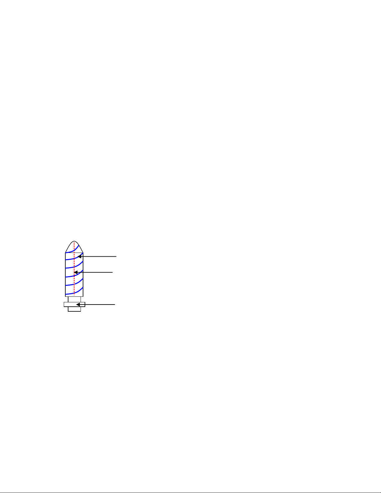
34. The received signal is received through the Antenna A10. The Tri Band antenna is
built up as per the diagram below and the received frequencies consist of:
a. EGSM 900 – 925.2Mhz – 959.8Mhz
b. GSM 1800 – 1805.2Mhz – 1879.8Mhz
c. GSM 1900 – 1930.2Mhz – 1989.8Mhz
35. The received frequency is then passed through Antenna matching LC circuitry,
and into the mechanical AUX RF switch A11. This is used as the Auxiliary RF
Phasing / test port. The input from / to the Main antenna is Pin 2 with the input
from the RF Switch U10 entering on Pin 1 (The Antenna is physically
disconnected once an external RF Cable is connected)
36. The received frequency is then fed into the RF Switch U10, Pin 16.
37. U10 is controlled by the following signals:
a. N_GSM_EXC_SW
b. GSM_EXC_SW
c. DCS_SW
d. N_DCS_SW
GSM Service Support
Motorola Proprietary Information
V66 – Level III Circuit Description
7
5V
U120
Internal Bias
From Patriot
5V
5V
Q202b
Q202a
5V
U110
U402b
Patriot
U700
RX_EN
N_EXC_EN
MAGIC
U201
N_DSC_SEL
N_GSM_SEL
RF_V2
U402a
DCS_SEL
PAC_275
N_TX_EN
Q203a
Q203b
EXC_EN
GSM_EXC_EN
GSM_EXC_SW
Q204b
Q204a
DCS_SW
N_DCS_SW
N_GSM_EXC_EN
N_GSM_EXC_SW
GSM Service Support
Motorola Proprietary Information
V66 – Level III Circuit Description
8
V4
V3
V2
V1
PATH
N_DCS_SW
1 0 0 0 (RX2) GSM, PCS receiver
DCS_SW
0 1 0
0
(RX1) DCS receiver
GSM_EXC_SW
0 0 1
0
(TX2) GSM transmitter
N_GSM_EXC_SW
0 0 0 1 (TX1) DCS, PCS transmitter
V4
RX1
RX2
V3
V2
TX1
TX2
V1
ANT
38. As can be seen the T/R switch operation is very simplistic with the control
signals, opening or closing the appropriate FET to allow input from either the
PCS / DCS TX path or EGSM 900 TX Path, output to the two RX paths or output
to the Antenna. Obviously the 2 RX paths are completely isolated during the TX
burst.
39. The Received frequency is then output to the appropriate frequency range output,
for EGSM 900 / PCS1900 the RX2 output is used Pin 12 and DCS1800 Pin 9.
40. These outputs are then fed into selective band-pass filters, which will attenuate all
other frequencies other than the band that we require.
a. For EGSM 900 – FL103
b. For GSM 1800 (DSC) – FL101
c. For GSM 1900 (PCS) – FL102
41. Each of the filter outputs are then matched using an LC tuning circuit.
42. The selected band filter outputs are then fed into the Front End IC U100.
43. The MC13709 Front End IC implements a Tri-band front-end receiver for EGSM, DCS &
PCS. The low band line up consists of an input low noise amplifier with the outputs driven
off the IC for inter-stage filtering and frequency matching. The signal then comes back
onto the IC into the RF amplifier of the Mixer. The mixer has a common LO stage to
improve the mixer output IF frequency performance. The LO is fed into the mixer through
44. If the L pin is connected to supply, then the LO input buffer is activated. However the LO
45. If the B pin is connected to ground then the 800/900MHz front end is activated and feeds
a buffer. The high band has an equivalent line up. LNA1 is targeted for use in the 900
MHz GSM spectrum. LNA2 for the DCS / PCS frequency ranges.
buffer will be on in additional states when LO is held low.
the IF output. If the BAND_SEL pin is connected to VCC then the 1800/1900MHz front
end is activated and feeds the IF output.
GSM Service Support
Motorola Proprietary Information

V66 – Level III Circuit Description
9
GSM1800
GSM 900
Matching
Circuit
Matching
13
18
12
20
24
9
3
4
IF+
IF-
Σ
Σ
From Main VCO
/ RX VCO
400 MHz
LNA1
LNA2A
MXR
MXR1
MXR2
Logic Control
B = N_GSM_SEL
E = RX_EN
L = RVCO
GSM1900
LNA2B
16
7
46. If the E pin is connected to supply, the remaining RF circuitry (selected by B) is enabled.
If E is connected to ground then the IC is placed in a low current standby mode, or has
the LO input buffer enabled dependent upon the L.
47. The circuit is supported by RF_V2
48. The operation of the Front End IC is as follows.
a) Signal from GSM / DCS / PCS Filters comes in on either pins 18, 13 or 16
respectively.
b) The appropriate signal is passed through its respective LNA and out to
matching network. Pins 12(O/P) + 9(I/P) for GSM 900, Pins 20(O/P)+
24(I/P) for DCS / PCS (FL100 removes any unwanted frequencies)
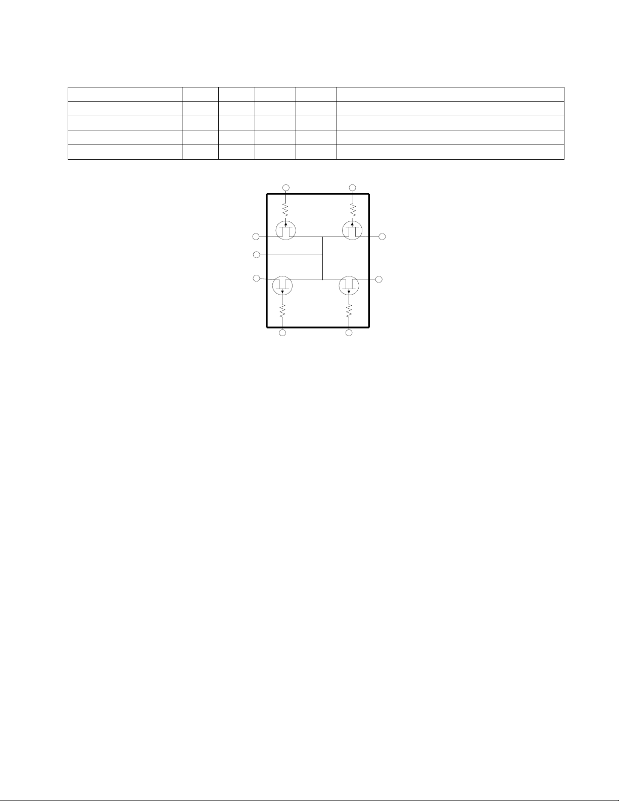
c) The next stage (MXR1 or MXR2) is made up of four ‘stacked’ modified
Darlington pairs. (See below)
GSM Service Support
Motorola Proprietary Information
V66 – Level III Circuit Description
10
O/P 2
O/P 1
+VCC
Floating I/P
Floating I/P
I/P from
Filters
Input from
Filters
Output 1
Output 2
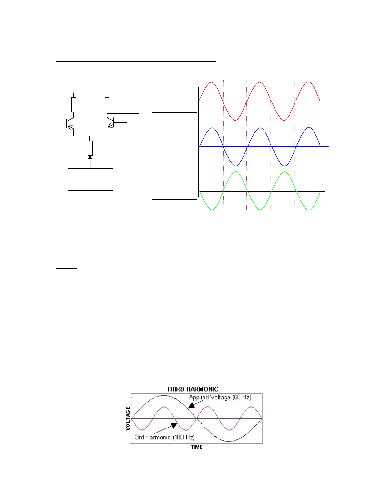
Darlington Pair shown in Front end IC Configuration
d) As can be seen the 2 outputs, which are 180 deg out of phase, are fed to the mixer
along with the Receiver VCO frequency.
e) These products are then mixed to give a + and – IF which is perfectly balanced and
fed to the SAW filter.
Notes:
Main reasons for front end IC:
Integration, less parts and less space (~49 parts less discrete equivalent)
No inter stage or buffer filtering required
<1uA shutdown current
Mixer Gain, 1dB(DCS) 4dB(GSM)
The reason for using a mixer and not a phase shifter on 1 line is that at 400 MHz
the output lines are very difficult to balance using the phase shifter which tends to
drift.
The SAW filter is the same as previous 400MHz products and is balanced to
accept the + and – IF’s
The reason for 2 IF’s is that this provides cancelling for the 3rd harmonic of the
13MHz system clock which at Channels 70 and 5 interferes with the received
GSM Service Support
Motorola Proprietary Information
 Loading...