Motorola V300, V525, V500, V600, V303 Service Manual
...
Consumer Solutions & Support
US Competency Center
600 North US Highway 45 Libertyville, Illinois 60048
Website: gs.mot.com
|
|
|
|
|
|
FSB Number: |
LVCCFSB2004-22 |
Author: |
Tony Bryan |
Date: |
March 4th, 2004 |
Total No. of Pages: |
3 |
Subject: |
GSM Triplets Rev. A PCB - ESD Improvement |
Model Affected: |
GSM V300, V303, V400 (SUGxxxxAA) |
|
GSM V500, V525 (SUGxxxxAA or SUGxxxxBA) |
Level of Repair: |
2 |
|
|
Problem
Service is aware of a field issue, identified during the 1st 200 NPI Analysis on the affected models listed above. Some units, returned with a customer complaint of “Invalid Battery”, were found to exhibit a lower than normal resistance on the OWB Line to the Neptune IC. Analysis revealed the root cause of this failure to be damage to the Neptune IC induced by ESD. Product Development identified, prior to launch, that all Triplets Rev. A PCB’s had a high susceptibility ESD related failure due to insufficient grounding of the SIM Chassis. A short-term corrective action was implemented, on all shipping product, adding a conductive 1.5mm pad to the back of the SIM Chassis to effectively ground the chassis. Unfortunately, after time in the field, the conductive pad can compress to the point where it no longer makes contact with the PCB Shielding thus leaving the phone susceptible to ESD related failure.
Solution
A re-design of the metal SIM Chassis (0188940N01) has been implemented in production as of 1/26/2004. The new (0188940N02) Rev. E design includes three metal fingers that extend into the housing and make contact with the PCB Shielding adequately grounding the SIM Chassis. For additional ESD Protection, a diode was added to the Rev. D PCB release.
Note: Also contained in the new Rev. E design is an improvement for connectivity of the Flip Assembly to PCB connector. See LVCCFSB2003-99 (Rev. A)
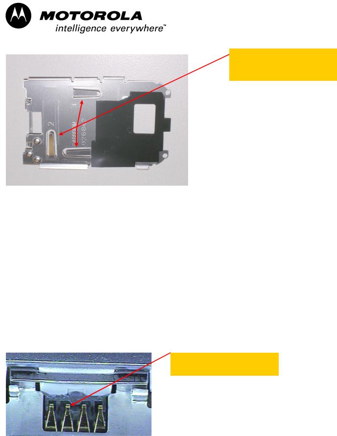
Diagram 1.0 below shows a sample of the (0188940N02) Rev. E SIM Chassis with the improved design.
MOTOROLA INTERNAL USE ONLY |
Page 1 |

Consumer Solutions & Support
US Competency Center
600 North US Highway 45 Libertyville, Illinois 60048
Website: gs.mot.com
Special Note:
New Design with Three Metal
Fingers to GND Chassis
Diagram 1.0 New (0188940N02) Rev. E SIM Chassis Design
Field Service Action
Customer Returns:
When servicing affected models of Triplets customer returns, regardless of customer complaint, then:
1.Disassemble the unit
2.Remove the existing Poron Pad from the Flip Assembly Connector
See LVCCFSB2003-99 (Rev. A)
3.Replace the existing metal SIM Chassis with the improved Rev. E Design
4.Reassemble and Relabel unit
5.Perform all necessary testing to ensure proper assembly
When servicing affected models of Triplets customer returns, with a customer complaint of “Invalid Battery”, then:
1.Power up the unit through the CE Connector with the battery removed
2.Probe the voltage on the OWB Line at M1700 (pin 3). The Voltage should be 2.7 VDC and will measure significantly less (approx 0.7 VDC) on failures with a damaged Neptune IC. See Diagram 2.0 below.
OWB Line:
M1700 Pin 3 = 2.7VDC
Diagram 3.0 Battery Contacts
MOTOROLA INTERNAL USE ONLY |
Page 2 |
 Loading...