

Motorola TP3006 Datasheet
1
TP3006MOTOROLA RF DEVICE DATA
The RF Line
The TP3006 is designed for cellular radio base station amplifiers up to 960
MHz. It incorporates high value emitter ballast resistors, gold metallizations and
offers a high degree of reliability and ruggedness. The TP3006 also features
input and output matching networks and high impedances. It can easily operate
in a full 870–960 MHz bandwidth in a simple circuit.
• Class AB Operation
• Specified 26 Volts, 960 MHz Characteristics
Output Power — 5 Watts
Gain — 9 dB min
Efficiency — 45% min
• Circuit board photomaster available upon request by contacting
RF Tactical Marketing in Phoenix, AZ.
MAXIMUM RATINGS
Rating Symbol Value Unit
Collector–Emitter Voltage V
CER
45 Vdc
Collector–Base Voltage V
CBO
55 Vdc
Emitter–Base Voltage V
EBO
3.5 Vdc
Collector–Current — Continuous I
C
2 Adc
Storage Temperature Range T
stg
– 40 to +100 °C
Operating Junction Temperature T
J
200 °C
Total Device Dissipation @ TC = 25°C
Derate above 25°C
P
D
25
0.14
Watts
W/°C
THERMAL CHARACTERISTICS
Characteristic Symbol Max Unit
Thermal Resistance, Junction to Case (1) R
θJC
7 °C/W
ELECTRICAL CHARACTERISTICS (T
C
= 25°C unless otherwise noted.)
Characteristic
Symbol Min Typ Max Unit
OFF CHARACTERISTICS
Collector–Emitter Breakdown Voltage
(IC = 15 mA, RBE = 75 Ω)
V
(BR)CER
45 — — Vdc
Emitter–Base Breakdown Voltage
(IE = 4 mAdc)
V
(BR)EBO
3.5 — — Vdc
Collector–Base Breakdown Voltage
(IC = 15 mAdc)
V
(BR)CBO
55 — — Vdc
Collector–Emitter Leakage
(VCE = 26 V, RBE = 75 Ω)
I
CER
— — 4 mA
ON CHARACTERISTICS
DC Current Gain
(IC = 0.5 Adc, VCE = 10 Vdc)
h
FE
15 — 100 —
NOTE: (continued)
1. Thermal resistance is determined under specified RF operating condition at temperature test point (see drawing of the package).
Order this document
by TP3006/D
SEMICONDUCTOR TECHNICAL DATA
5 W, 870–960 MHz
RF POWER TRANSISTOR
NPN SILICON
CASE 319–07, STYLE 2
Motorola, Inc. 1994
REV 6
TP3006
2
MOTOROLA RF DEVICE DATA
ELECTRICAL CHARACTERISTICS — continued (T
C
= 25°C unless otherwise noted.)
Characteristic
Symbol Min Typ Max Unit
DYNAMIC CHARACTERISTICS
Output Capacitance
(VCB = 26 V, IE = 0, f = 1 MHz )
C
ob
— 8.5 — pF
FUNCTIONAL TESTS IN CW
Common–Emitter Amplifier Power Gain
(VCC = 26 V, P
out
= 5 W, ICQ = 50 mA, f = 960 MHz)
G
p
9 10.5 — dB
Collector Efficiency
(VCC = 26 V, P
out
= 5 W, IQ = 50 mA, f = 960 MHz)
h 45 50 — %
Input Overdrive (no degradation in P
out
)
(VCC = 26 V, IQ = 50 mA, f = 960 MHz)
P
in
3 — — dB
FUNCTIONAL TESTS IN 2 TONES
3rd Order Intermodulation
(VCC = 26 V, P
peak
= 5 W, ICQ = 50 mA, f = 900 MHz)
IMD3 — – 46 — dB
5th Order Intermodulation
(VCC = 26 V, P
peak
= 5 W, ICQ = 50 mA, f = 900 MHz)
IMD5 — – 46 — dB
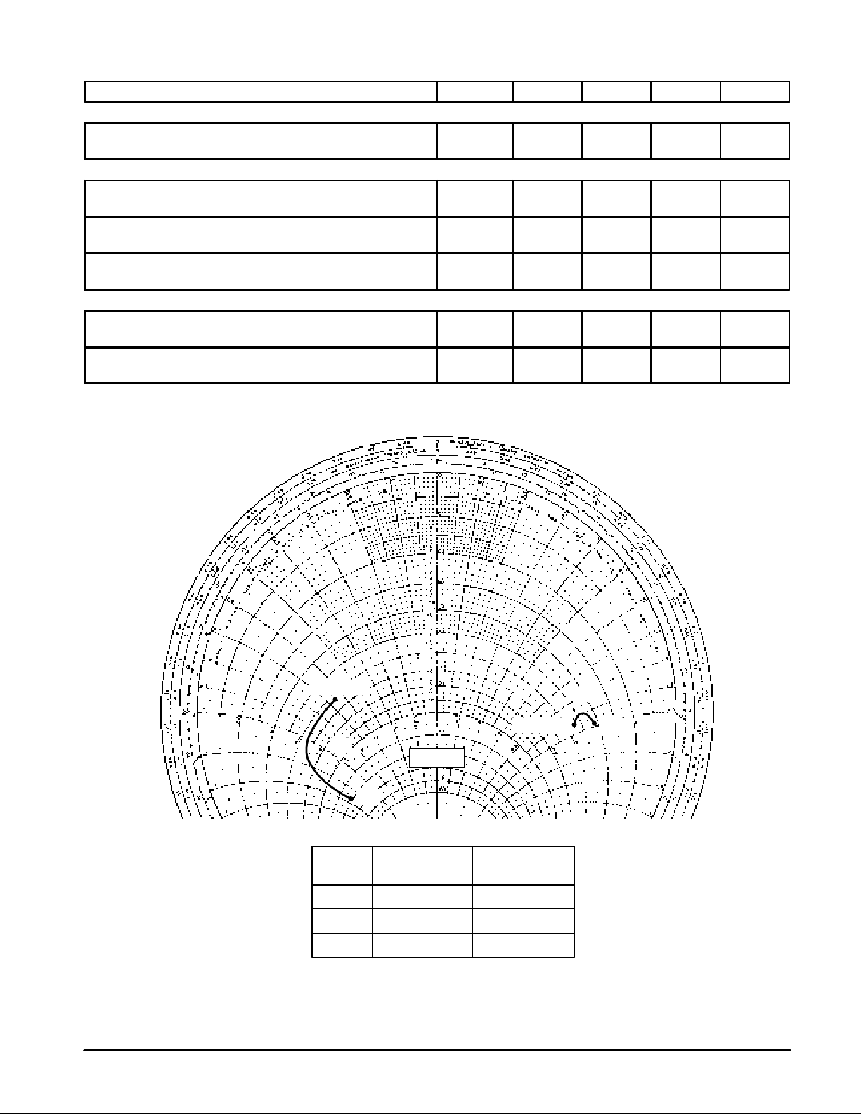
Figure 1. Series Equivalent Input and Output Impedances
f
(MHz)
Z
in
(Ω)
Z
OL
(Ω)
870
900
960
6.26 – j6.40
14.8 – j12.9
7.40 – j12.3
5.22 + j9.47
4.17+ j9.02
4.21 + j9.91
P
out
= 5 W (CW), VCE = 26 V, ICQ = 50 mA
f = 870 MHz
Z
OL
Z
in
960
Zo = 10
Ω
f = 870 MHz
960
 Loading...