

Motorola TP3005 Datasheet
1
TP3005MOTOROLA RF DEVICE DATA
The RF Line
The TP3005 is designed for 960 MHz base stations in both analog and digital
applications. It incorporates high value emitter ballast resistors, gold metallizations and offers a high degree of reliability and ruggedness.
• Specified 26 Volts, 960 MHz Characteristics
Output Power = 4.0 Watts
Minimum Gain = 8.5 dB
Class AB
IQ = 60 mA
• Circuit board photomaster available upon request by contacting
RF Tactical Marketing in Phoenix, AZ.
MAXIMUM RATINGS
Rating Symbol Value Unit
Collector–Emitter Voltage V
CER
40 Vdc
Collector–Base Voltage V
CBO
48 Vdc
Emitter–Base Voltage V
EBO
4.0 Vdc
Collector Current — Continuous I
C
2.0 Adc
Total Device Dissipation @ TC = 25°C
Derate above 25°C
P
D
25
0.2
Watts
W/°C
Storage Temperature Range T
stg
–65 to +150 °C
Operating Junction Temperature T
J
200 °C
THERMAL CHARACTERISTICS
Characteristic Symbol Max Unit
Thermal Resistance, Junction to Case (1) at 70°C Case R
θJC
7.0 °C/W
ELECTRICAL CHARACTERISTICS (T
C
= 25°C unless otherwise noted.)
Characteristic
Symbol Min Typ Max Unit
OFF CHARACTERISTICS
Collector–Emitter Breakdown Voltage
(IC = 15 mA, RBE = 75 Ω)
V
(BR)CER
45 — — Vdc
Emitter–Base Breakdown Voltage
(IC = 3.0 mAdc)
V
(BR)EBO
4.0 — — Vdc
Collector–Base Breakdown Voltage
(IE = 15 mAdc)
V
(BR)CBO
55 — — Vdc
Collector–Emitter Leakage
(VCE = 26 V, RBE = 75 Ω)
I
CER
— — 3.0 mA
ON CHARACTERISTICS
DC Current Gain
(IC = 0.5 Adc, VCE = 10 Vdc)
h
FE
15 — 100 —
NOTE: (continued)
1. Thermal resistance is determined under specified RF operating condition.
Order this document
by TP3005/D
SEMICONDUCTOR TECHNICAL DATA
4.0 W, 960 MHz
UHF POWER
TRANSISTOR
NPN SILICON
CASE 319–07, STYLE 2
Motorola, Inc. 1994
REV 6
TP3005
2
MOTOROLA RF DEVICE DATA
ELECTRICAL CHARACTERISTICS — continued (T
C
= 25°C unless otherwise noted.)
Characteristic
Symbol Min Typ Max Unit
DYNAMIC CHARACTERISTICS
Output Capacitance
(VCB = 26 V, IE = 0, f = 1.0 MHz)
C
ob
7.5 — 12.5 pF
FUNCTIONAL TESTS
Common–Emitter Amplifier Power Gain
(VCC = 26 V, P
out
= 4.0 W, ICQ = 60 mA, f = 960 MHz)
G
p
8.5 9.5 — dB
Load Mismatch
(VCC = 26 V, P
out
= 4.0 W, ICQ = 60 mA, Load VSWR = 5:1,
at all phase angles)
ψ
No Degradation in Output Power
Before and After Test
Collector Efficiency
(VCC = 26 V, P
out
= 4.0 W, f = 960 MHz)
η
c
50 55 — %
Power Saturation Pin = 1.0 W P
sat
7.0 — — W
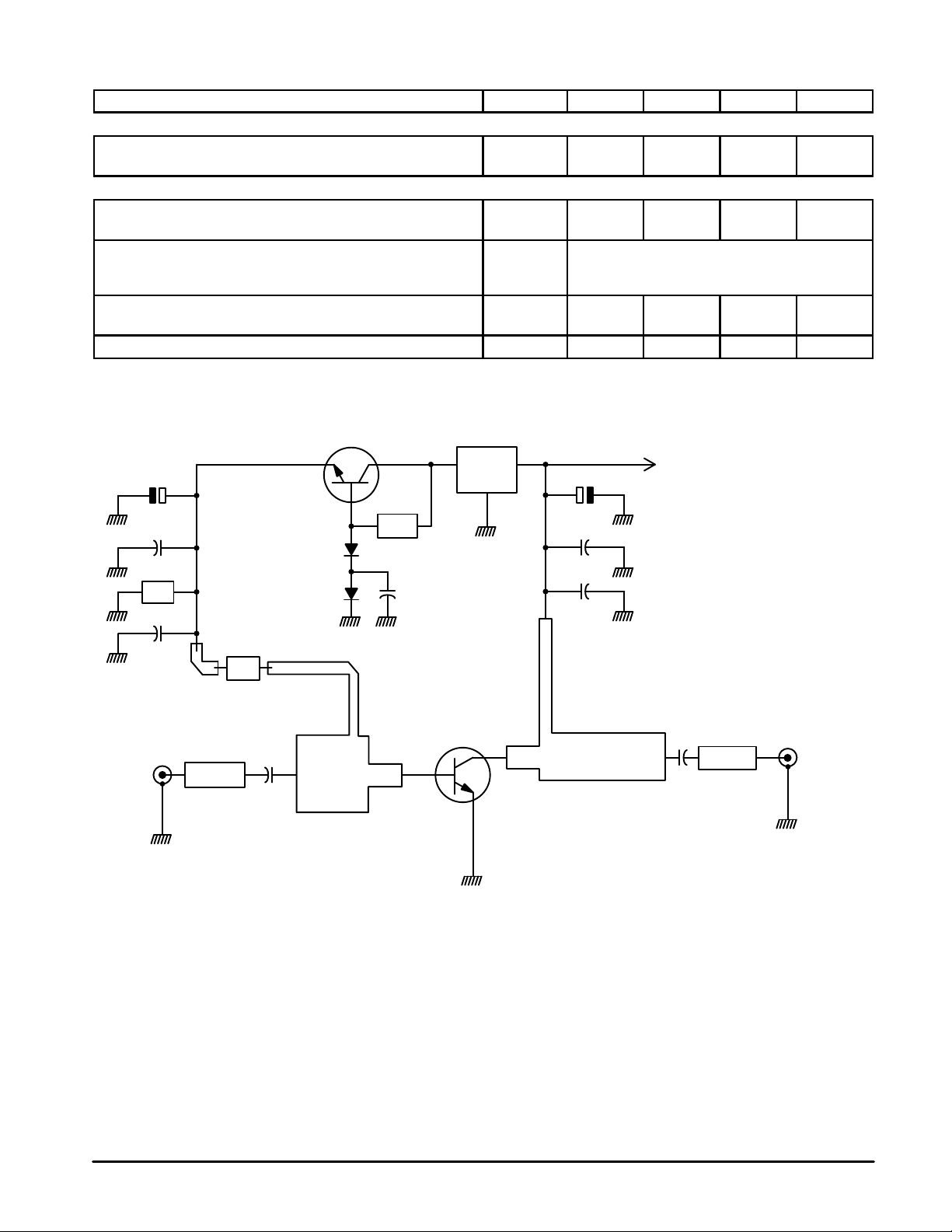
Figure 1. 960 MHz Test Circuit
*Contact with RF Transistor
C1 — Capacitor Chip 0805 22 pF 5%
C2, C3, C6, C8 — Capacitor Chip 0805 330 pF 5%
C4, C7 — Capacitor Chip 0805 15 nF 5%
C5, C9 — Capacitor Chip 0805 6.0, 8.0 nF 35 V
D1, D2 — SMD Diode
R1 — Chip Resistor 2.2 Ω 1206 5%
R2 — Chip Resistor 51 Ω 0805 5%
R3 — Chip Resistor 470 Ω 0805 5%
R3 — to be adjusted for IQ = 60 mA
T1 — SMD Transistor BCX54 or Similar
T3 — Voltage Regulator 7805
Board Material — 0.8 mm, Epoxy Glass, Cu Clad, 2 Sides,
35 µm Thick
RF INPUT
50
Ω
RF OUTPUT
50
Ω
D.U.T.
C5
C4
C3
R2
R1
C1
D1
D2*
C6
R3
T1
T3
+V
CC
+
C9
C8
C7
C2
+
 Loading...