Motorola TL594CDR2, TL594CD, TL594IN, TL594CN Datasheet

The TL594 is a fixed frequency, pulse width modulation control circuit
designed primarily for Switchmode power supply control.
• Complete Pulse Width Modulation Control Circuitry
• On–Chip Oscillator with Master or Slave Operation
• On–Chip Error Amplifiers
• On–Chip 5.0 V Reference, 1.5% Accuracy
• Adjustable Deadtime Control
• Uncommitted Output Transistors Rated to 500 mA Source or Sink
• Output Control for Push–Pull or Single–Ended Operation
• Undervoltage Lockout
Order this document by TL594/D
PRECISION SWITCHMODE
PULSE WIDTH MODULATION
CONTROL CIRCUIT
SEMICONDUCTOR
TECHNICAL DATA
D SUFFIX
PLASTIC PACKAGE
CASE 751B
(SO–16)
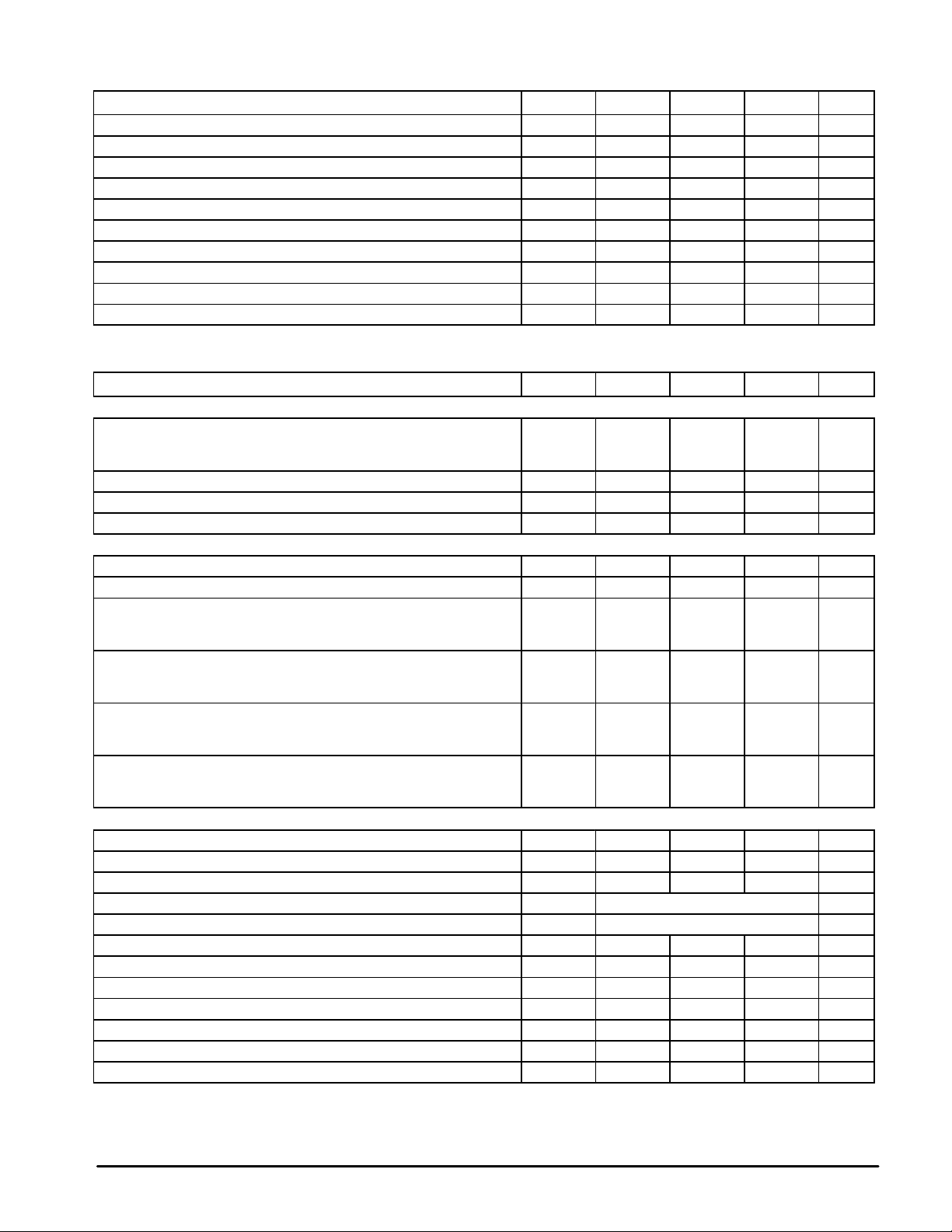
MAXIMUM RATINGS
unless otherwise noted.)
Power Supply Voltage V
Collector Output Voltage VC1,
Collector Output Current
(each transistor) (Note 1)
Amplifier Input Voltage Range V
Power Dissipation @ TA ≤ 45°C P
Thermal Resistance,
Junction–to–Ambient
Operating Junction Temperature T
Storage Temperature Range T
Operating Ambient Temperature Range
TL594ID, CN
TL594CD, IN
Derating Ambient Temperature T
NOTES: 1.Maximum thermal limits must be observed.
(Full operating ambient temperature range applies,
Rating
Symbol Value Unit
IC1, I
N SUFFIX
PLASTIC PACKAGE
CASE 648
PIN CONNECTIONS
Noninv
1
Input
Input
Compen/PWN
Comp Input
Deadtime
CC
V
C2
C2
IR
D
R
θJA
J
stg
T
A
A
42 V
42 V
500 mA
–0.3 to +42 V
1000 mW
80 °C/W
125 °C
–55 to +125 °C
°C
0 to +70
–25 to +85
45 °C
Control
Ground
ORDERING INFORMATION
Device
TL594CD
TL594CN
TL594IN Plastic
+
Error
Amp
Inv
–
2
3
≈
0.1 V
4
C
5
T
Oscillator
R
6
T
7
C1
89
Operating
Temperature Range
TA = 0° to +70°C
TA = –25° to +85°C
1
2
V
CC
Q1
(Top View)
Error
Amp
5.0 V
REF
+
–
Q2
Noninv
16
Input
Inv
15
Input
V
14
ref
Output
13
Control
V
12
CC
C2
11
E2
10
E1
Package
SO–16
Plastic
MOTOROLA ANALOG IC DEVICE DATA
Motorola, Inc. 1996 Rev 0
1

TL594
RECOMMENDED OPERATING CONDITIONS
Characteristics Symbol Min Typ Max Unit
Power Supply Voltage V
Collector Output Voltage VC1, V
Collector Output Current (Each transistor) IC1, I
Amplified Input Voltage V
Current Into Feedback Terminal l
Reference Output Current l
Timing Resistor R
Timing Capacitor C
Oscillator Frequency f
PWM Input Voltage (Pins 3, 4, 13) – 0.3 – 5.3 V
CC
C2
C2
in
fb
ref
T
T
osc
7.0 15 40 V
– 30 40 V
– – 200 mA
0.3 – VCC – 2.0 V
– – 0.3 mA
– – 10 mA
1.8 30 500 kΩ
0.0047 0.001 10 µF
1.0 40 200 kHz
ELECTRICAL CHARACTERISTICS (V
For typical values TA = 25°C, for min/max values TA is the operating ambient temperature range that applies, unless otherwise noted.
Characteristics
REFERENCE SECTION
Reference Voltage
(IO = 1.0 mA, TA = 25°C)
(IO = 1.0 mA)
Line Regulation (VCC = 7.0 V to 40 V) Reg
Load Regulation (IO = 1.0 mA to 10 mA) Reg
Short Circuit Output Current (V
OUTPUT SECTION
Collector Off–State Current (VCC = 40 V, VCE = 40 V) I
Emitter Off–State Current (VCC = 40 V, VC = 40 V, VE = 0 V) I
Collector–Emitter Saturation Voltage (Note 2)
Common–Emitter (VE = 0 V, IC = 200 mA)
Emitter–Follower (VC = 15 V, IE = –200 mA)
Output Control Pin Current
Low State (VOC ≤ 0.4 V)
High State (VOC = V
Output Voltage Rise T ime
Common–Emitter (See Figure 13)
Emitter–Follower (See Figure 14)
Output Voltage Fall T ime
Common–Emitter (See Figure 13)
Emitter–Follower (See Figure 14)
ERROR AMPLIFIER SECTION
Input Offset Voltage (VO
Input Offset Current (VO
Input Bias Current (VO
Input Common Mode Voltage Range (VCC = 40 V, TA = 25°C) V
Inverting Input Voltage Range V
Open Loop Voltage Gain (∆VO = 3.0 V, VO = 0.5 V to 3.5 V, RL = 2.0 kΩ) A
Unity–Gain Crossover Frequency (VO = 0.5 V to 3.5 V, RL = 2.0 kΩ) f
Phase Margin at Unity–Gain (VO = 0.5 V to 3.5 V, RL = 2.0 kΩ) φm – 65 – deg.
Common Mode Rejection Ratio (VCC = 40 V) CMRR 65 90 – dB
Power Supply Rejection Ratio (∆VCC = 33 V, VO = 2.5 V, RL = 2.0 kΩ) PSRR – 100 – dB
Output Sink Current (VO
Output Source Current (VO
NOTE: 2. Low duty cycle pulse techniques are used during test to maintain junction temperature as close to ambient temperature as possible.
ref
(Pin 3)
= 0 V) I
ref
)
= 2.5 V) V
(Pin 3)
= 2.5 V) I
(Pin 3)
= 2.5 V) I
= 0.7 V) IO– 0.3 0.7 – mA
(Pin 3)
= 3.5 V) IO+ –2.0 –4.0 – mA
(Pin 3)
= 15 V, CT = 0.01 µF, RT = 12 kΩ, unless otherwise noted.)
CC
Symbol Min Typ Max Unit
V
SC
C(off)
E(off)
V
SAT(C)
V
SAT(E)
I
OCL
I
OCH
IO
IB
ICR
IR(INV)
VOL
ref
line
load
t
r
t
f
IO
C
4.925
4.9
– 2.0 25 mV
– 2.0 15 mV
15 40 75 mA
– 2.0 100 µA
– – –100 µA
–
–
–
–
–
–
–
–
– 2.0 10 mV
– 5.0 250 nA
– –0.1 –1.0 µA
70 95 – dB
– 700 – kHz
5.0
–
1.1
1.5
0.1
2.0
100
100
40
40
0 to VCC–2.0 V
–0.3 to VCC–2.0 V
5.075
5.1
1.3
2.5
–
20
200
200
100
100
V
V
µA
ns
ns
2
MOTOROLA ANALOG IC DEVICE DATA

TL594
ELECTRICAL CHARACTERISTICS (V
For typical values TA = 25°C, for min/max values TA is the operating ambient temperature range that applies, unless otherwise noted.
Characteristics
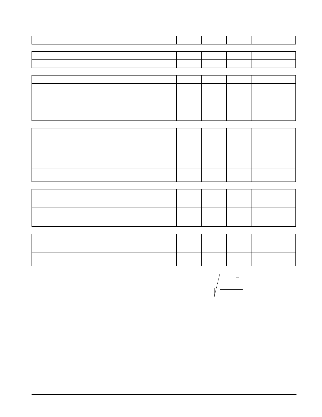
PWM COMPARATOR SECTION (Test Circuit Figure 11)
Input Threshold Voltage (Zero Duty Cycle) V
Input Sink Current (V
DEADTIME CONTROL SECTION (Test Circuit Figure 11)
Input Bias Current (Pin 4) (V
Maximum Duty Cycle, Each Output, Push–Pull Mode
(V
= 0 V, CT = 0.01 µF, RT = 12 kΩ)
Pin 4
(V
= 0 V, CT = 0.001 µF, RT = 30 kΩ)
Pin 4
Input Threshold Voltage (Pin 4)
(Zero Duty Cycle)
(Maximum Duty Cycle)
OSCILLATOR SECTION
Frequency
(CT = 0.001 µF, RT = 30 kΩ)
(CT = 0.01 µF, RT = 12 kΩ, TA = 25°C)
(CT = 0.01 µF, RT = 12 kΩ, TA = T
Standard Deviation of Frequency* (CT = 0.001 µF, RT = 30 kΩ) σf
Frequency Change with Voltage (VCC = 7.0 V to 40 V, TA = 25°C) ∆f
Frequency Change with Temperature
(∆TA = T
UNDERVOLTAGE LOCKOUT SECTION
Turn–On Threshold (VCC Increasing, I
TA = 25°C
TA = T
Hysteresis
TL594C,I
TL594M
TOTAL DEVICE
Standby Supply Current (Pin 6 at V
(VCC = 15 V)
(VCC = 40 V)
Average Supply Current (V
VCC = 15 V, See Figure 11)
low
low
to T
to T
high
= 0.7 V) I
Pin 3
= 0 V to 5.25 V) IIB
Pin 4
low
, CT = 0.01 µF, RT = 12 kΩ)
high
, All other inputs and outputs open)
ref
= 2.0 V, CT = 0.01 µF, RT = 12 kΩ,
Pin 4
= 15 V, CT = 0.01 µF, RT = 12 kΩ, unless otherwise noted.)
CC
Symbol Min Typ Max Unit
TH
I–
(DT)
DC
max
V
TH
f
osc
to T
ref
)
high
= 1.0 mA)
osc
(∆V) – 0.2 1.0 %
osc
∆f
(∆T) – 4.0 – %
osc
V
th
V
H
I
CC
– 3.6 4.5 V
0.3 0.7 – mA
– –2.0 –10 µA
45
–
–
0
–
9.2
9.0
– 1.5 – %
4.0
3.5
100
50
–
–
– 11 –
48
45
2.8
–
40
10
–
5.2
–
150
150
8.0
8.0
50
–
3.3
–
–
10.8
12
6.0
6.5
300
300
15
18
%
V
kHz
V
mV
mA
mA
* Standard deviation is a measure of the statistical distribution about the mean as derived from the formula, σ
MOTOROLA ANALOG IC DEVICE DATA
N
Σ (Xn – X
n = 1
N – 1
2
)
3

TL594
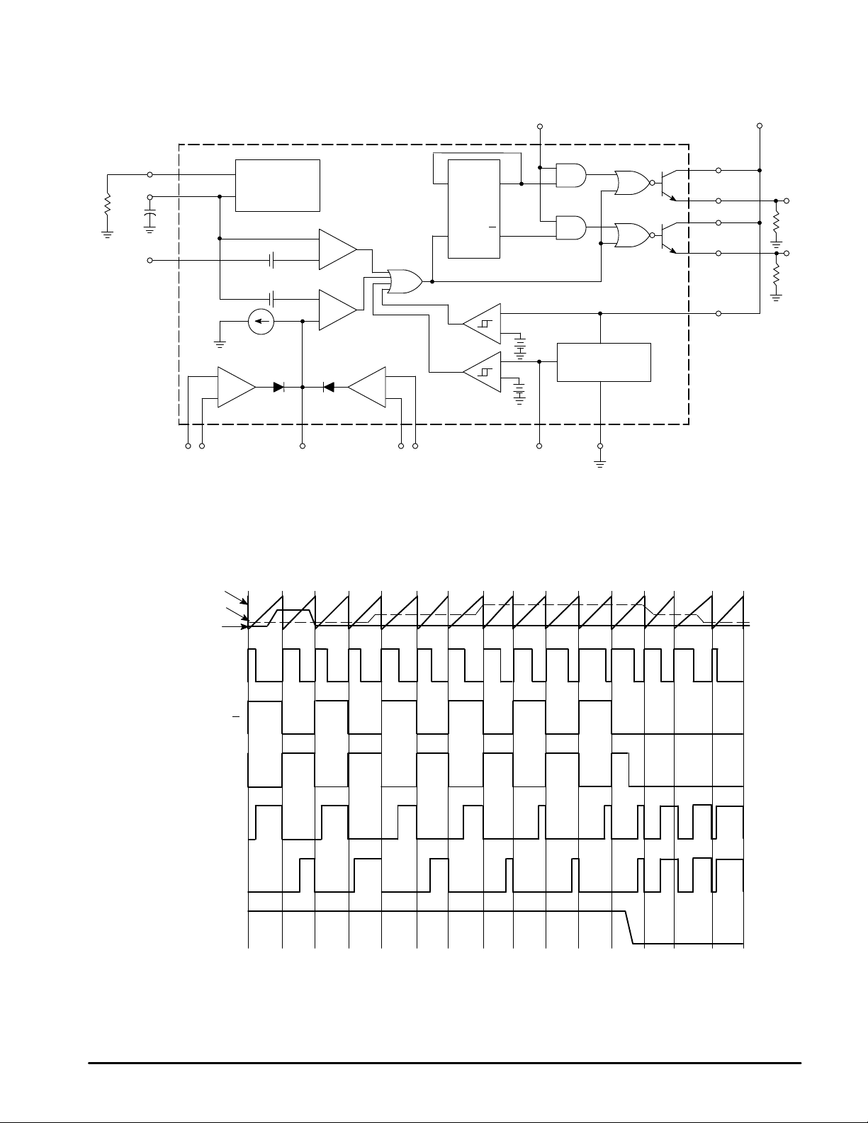
Figure 1. Representative Block Diagram
R
T
6
5
C
T
4
Deadtime
Control
Output Control
13
D
Ck
UV
Flip–
Flop
Q
Q
–
+
–
+
3.5V
4.9V
Ref.
Output
Reference
Regulator
Gnd
Oscillator
Deadtime
Comparator
≈
0.12V
≈
0.7V
0.7mA
+
1
–
12 3 1516 14 7
Error Amp
1
Feedback PWM
Comparator Input
–
+
–
+
PWM
Comparator
+
2
–
Error Amp
This device contains 46 active transistors.
Lockout
2
Q1
Q2
8
9
11
10
12
V
CC
V
CC
Capacitor C
Feedback/PWM Comp.
Deadtime Control
T
Flip–Flop
Clock Input
Flip–Flop
Q
Flip–Flop
Q
Output Q1
Emitter
Output Q2
Emitter
Output
Control
Figure 2. Timing Diagram
4
MOTOROLA ANALOG IC DEVICE DATA
 Loading...