MOTOROLA SN74LS298D, SN74LS298DR2, SN74LS298ML1, SN74LS298ML2, SN74LS298N Datasheet

Semiconductor Components Industries, LLC, 1999
December, 1999 – Rev. 6
1 Publication Order Number:
SN74LS298/D
SN74LS298
Quad 2-Input Multiplexer
with Storage
The SN74LS298 is a Quad 2-Port Register. It is the logical
equivalent of a quad 2-input multiplexer followed by a quad 4-bit
edge-triggered register. A Common Select input selects between two
4-bit input ports (data sources.) The selected data is transferred to the
output register synchronous with the HIGH to LOW transition of the
Clock input.
The LS298 is fabricated with the Schottky barrier process for high
speed and is completely compatible with all ON Semiconductor TTL
families.
• Select From Two Data Sources
• Fully Edge-Triggered Operation
• Typical Power Dissipation of 65 mW
• Input Clamp Diodes Limit High Speed Termination Effects
GUARANTEED OPERATING RANGES
Symbol Parameter Min Typ Max Unit
V
CC
Supply Voltage 4.75 5.0 5.25 V
T
A
Operating Ambient
T emperature Range
0 25 70 °C
I
OH
Output Current – High –0.4 mA
I
OL
Output Current – Low 8.0 mA
LOW
POWER
SCHOTTKY
Device Package Shipping
ORDERING INFORMATION
SN74LS298N 16 Pin DIP 2000 Units/Box
SN74LS298D 16 Pin
SOIC
D SUFFIX
CASE 751B
http://onsemi.com
2500/Tape & Reel
PLASTIC
N SUFFIX
CASE 648
16
1
16
1

SN74LS298
http://onsemi.com
2
CONNECTION DIAGRAM DIP (TOP VIEW)
Common Select Input
Clock (Active LOW Going Edge) Input
Data Inputs from Source 0
Data Inputs from Source 1
Register Outputs
S
CP
I0a – I
0d
I1a – I
1d
Qa – Q
d
0.5 U.L.
0.5 U.L.
0.5 U.L.
0.5 U.L.
10 U.L.
0.25 U.L.
0.25 U.L.
0.25 U.L.
0.25 U.L.
5 U.L.
NOTES:
a) 1 TTL Unit Load (U.L.) = 40 mA HIGH/1.6 mA LOW.
HIGH LOW
(Note a)LOADING
PIN NAMES
LOGIC SYMBOL
NOTE:
The Flatpak version has the same
pinouts (Connection Diagram) as
the Dual In-Line Package.
14 13 12 11 10 9
123456
7
16 15
8
V
CC
I
1b
QaQbQcQ
d
SCP I
0c
I1aI
0aI0bI1cI1dI0d
GND
VCC = PIN 16
GND = PIN 8
324195 76
15 14 13 12
10
11
I
0aI1aI0bI1bI0cI1cI0dI1d
S
CP
Q
a
Q
b
Q
c
Q
d

SN74LS298
http://onsemi.com
3
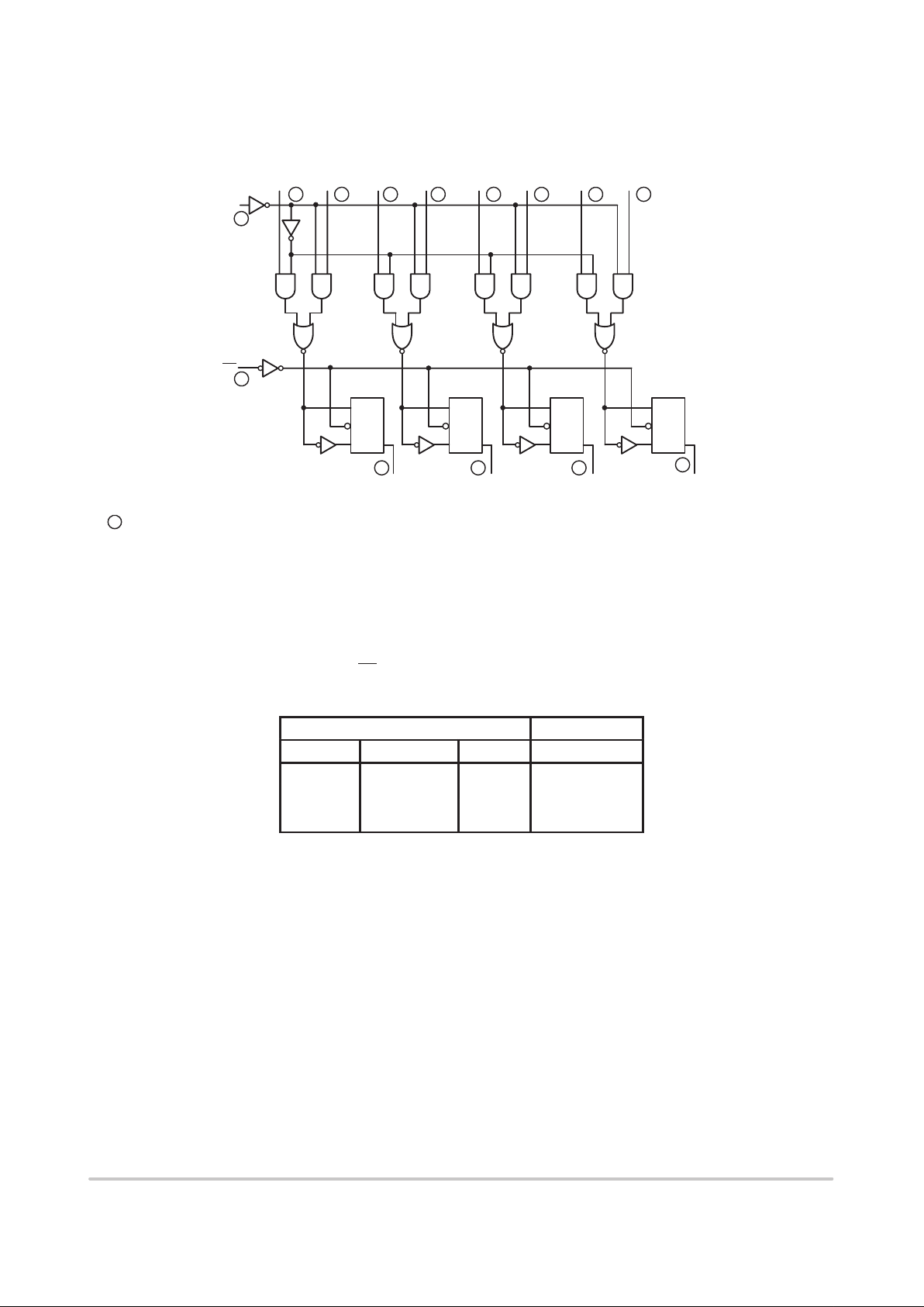
LOGIC OR BLOCK DIAGRAM
S
I
1a
I
0a
I
1b
I
0b
I
1c
I
0c
I
1d
I
0d
CP
R
CP
SQ
a
R
CP
SQ
b
Q
a
Q
b
Q
c
Q
d
14
12 673 4 5 9
11
12
10
1315
VCC = PIN 16
GND = PIN 8
= PIN NUMBERS
R
CP
SQ
c
R
CP
SQ
d
FUNCTIONAL DESCRIPTION
The LS298 is a high speed Quad 2-Port Register. It selects
four bits of data from two sources (ports)under the control
of a Common Select Input (S). The selected data is
transferred to the 4-bit output register synchronous with the
HIGH to LOW transition of the Clock input (CP
). The 4-bit
output register is fully edge-triggered. The Data inputs (I)
and Select input (S) must be stable only one setup time prior
to the HIGH to LOW transition of the clock for predictable
operation.
TRUTH TABLE
INPUTS OUTPUT
S I
0
I
1
Q
I I X L
I h X H
h X I L
h X h H
L = LOW Voltage Level
H = HIGH Voltage Level
X = Don’t Care
I = LOW Voltage Level one setup time prior to the HIGH to LOW clock transition.
h = HIGH Voltage Level one setup time prior to the HIGH to LOW clock transition.
 Loading...