

MOTOROLA SN74LS258BN, SN74LS258BD, SN74LS258BDR2, SN74LS258BMEL, SN74LS258BML1 Datasheet
...
Semiconductor Components Industries, LLC, 1999
December, 1999 – Rev. 6
1 Publication Order Number:
SN74LS257B/D
SN74LS257B SN74LS258B
Quad 2-Input Multiplexer
with 3-State Outputs
The LSTTL /MSI SN74LS257B and the SN74LS258B are Quad
2-Input Multiplexers with 3-state outputs. Four bits of data from two
sources can be selected using a Common Data Select input. The four
outputs present the selected data in true (non-inverted) form. The
outputs may be switched to a high impedance state with a HIGH on the
common Output Enable (E
O
) Input, allowing the outputs to interface
directly with bus oriented systems. It is fabricated with the Schottky
barrier diode process for high speed and is completely compatible with
all ON Semiconductor TTL families.
• Schottky Process For High Speed
• Multiplexer Expansion By Tying Outputs T ogether
• Non-Inverting 3-State Outputs
• Input Clamp Diodes Limit High Speed Termination Effects
• Special Circuitry Ensures Glitch Free Multiplexing
• ESD > 3500 Volts
GUARANTEED OPERATING RANGES
Symbol Parameter Min Typ Max Unit
V
CC
Supply Voltage 4.75 5.0 5.25 V
T
A
Operating Ambient
T emperature Range
0 25 70 °C
I
OH
Output Current – High –2.6 mA
I
OL
Output Current – Low 24 mA
LOW
POWER
SCHOTTKY
Device Package Shipping
ORDERING INFORMATION
SN74LS257BN 16 Pin DIP 2000 Units/Box
SN74LS257BD 16 Pin
SOIC
D SUFFIX
CASE 751B
http://onsemi.com
2500/Tape & Reel
PLASTIC
N SUFFIX
CASE 648
16
1
16
1
SN74LS258BN 16 Pin DIP 2000 Units/Box
SN74LS258BD 16 Pin
2500/Tape & Reel
SN74LS257B SN74LS258B
http://onsemi.com
2
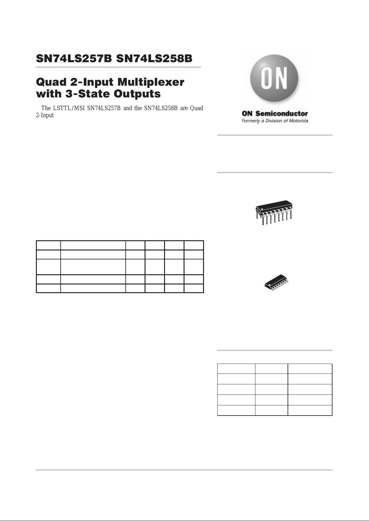
CONNECTION DIAGRAM DIP (TOP VIEW)
NOTE:
The Flatpak version has the same
pinouts (Connection Diagram) as
the Dual In-Line Package.
14 13 12 11 10 9
123456
7
16 15
8
V
CC
S
E
0I0cI1cZc
I
1d
I
0d
Z
d
I0aI
1aZaI0bI1b
ZbGND
SN74LS257B
SN74LS258B
VCC = PIN 16
GND = PIN 8
14 13 12 11 10 9
123456
7
16 15
8
V
CC
S
E
0I0cI1cZc
I
1d
I
0d
Z
d
I0aI
1aZaI0bI1b
ZbGND
SN74LS257B SN74LS258B
http://onsemi.com
3
LOGIC DIAGRAMS
SN74LS257B
E
0
I
0a
I
1a
I
0b
I
1b
I
0c
I
1c
I
0d
I
1d
S
Z
a
Z
b
Z
c
Z
d
SN74LS258B
VCC = PIN 16
GND = PIN 8
= PIN NUMBERS
E
0
I
0a
I
1a
I
0b
I
1b
I
0c
I
1c
I
0d
I
1d
S
Z
a
Z
b
Z
c
Z
d
14
1
2
6
7
3
4
5
9
11
12
10
13
15
14
1
2
6
3
5
11
10
13
15
7
4 912

SN74LS257B SN74LS258B
http://onsemi.com
4
FUNCTIONAL DESCRIPTION
The LS257B and LS258B are Quad 2-Input Multiplexers
with 3-state outputs. They select four bits of data from two
sources each under control of a Common Data Select Input.
When the Select Input is LOW , the I
0
inputs are selected and
when Select is HIGH, the I1 inputs are selected. The data on
the selected inputs appears at the outputs in true
(non-inverted) form for the LS257B and in the inverted form
for the LS258B.
The LS257B and LS258B are the logic implementation of
a 4-pole, 2-position switch where the position of the switch
is determined by the logic levels supplied to the Select Input.
The logic equations for the outputs are shown below:
When the Output Enable Input (E
0
) is HIGH, the outputs
are forced to a high impedance “off” state. If the outputs are
tied together, all but one device must be in the high
impedance state to avoid high currents that would exceed the
maximum ratings. Designers should ensure that Output
Enable signals to 3-state devices whose outputs are tied
together are designed so there is no overlap.
LS257B
Z
a
= E0 • (I1a • S + I0a • S) Zb = E0 • (I1b • S + I0b • S)
Z
c
= E0 • (I1c • S + I0c • S) Z
d
= E0 • (I1d • S + I0d • S)
LS258B
Z
a
= E0 • (I1a • S + I0a • S) Zb = E0 • (I1b • S + I0b • S)
Z
c
= E0 • (I1c • S + I0c • S) Zd = E0 • (I1d • S + I
0d
• S)
TRUTH TABLE
OUTPUT
ENABLE
SELECT
INPUT
DATA
INPUTS
OUTPUTS
LS257B
OUTPUTS
LS258B
E
O
S I
0I1
Z Z
H X X X (Z) (Z)
L H X LL H
L H X HH L
L L L XL H
L L H X H L
H = HIGH Voltage Level
L = LOW Voltage Level
X = Don’t Care
(Z) = High Impedance (off)

SN74LS257B SN74LS258B
http://onsemi.com
5
DC CHARACTERISTICS OVER OPERATING TEMPERATURE RANGE (unless otherwise specified)
Limits
Symbol Parameter
Min Typ Max
Unit Test Conditions
V
IH
Input HIGH Voltage 2.0 V
Guaranteed Input HIGH Voltage for
All Inputs
V
IL
Input LOW Voltage
0.8
V
Guaranteed Input LOW Voltage for
All Inputs
V
IK
Input Clamp Diode Voltage –0.65 –1.5 V VCC = MIN, IIN = –18 mA
V
OH
Output HIGH Voltage 2.4 3.1 V
VCC = MIN, IOH = MAX, VIN = V
IH
or VIL per Truth Table
p
0.25 0.4 V IOL = 12 mA
VCC = VCC MIN,
VOLOutput LOW Voltage
0.35 0.5 V IOL = 24 mA
V
IN
=
V
IL
or
V
IH
per Truth Table
I
OZH
Output Off Current — HIGH 20 µA VCC = MAX, V
OUT
= 2.7 V
I
OZL
Output Off Current — LOW –20 µA VCC = MAX, V
OUT
= 0.4 V
I
IH
Input HIGH Current
Other Inputs
S Inputs
20
40
µA VCC = MAX, VIN = 2.7 V
IH
Other Inputs
S Inputs
0.1
0.2
mA VCC = MAX, VIN = 7.0 V
I
IL
Input LOW Current
All Inputs
–0.4 mA VCC = MAX, VIN = 0.4 V
I
OS
Short Circuit Current (Note 1) –30 –130 mA VCC = MAX
Power Supply Current
Total, Output HIGH
LS257B
LS258B
10
9.0
mA
I
CC
Total, Output LOW
LS257B
LS258B
16
14
mA
VCC = MAX
Total, Output 3-State
LS257B
LS258B
19
16
mA
Note 1: Not more than one output should be shorted at a time, nor for more than 1 second.
AC CHARACTERISTICS (T
A
= 25°C, VCC = 5.0 V) See SN74LS251 for Waveforms
Limits
Symbol Parameter
Min Typ Max
Unit Test Conditions
t
PLH
t
PHL
Propagation Delay , Data to Output
10
12
13
15
ns Figures 1 & 2
p
t
PLH
t
PHL
Propagation Delay , Select to Output
14
14
21
21
ns Figures 1 & 2
C
L
= 45
pF
t
PZH
Output Enable Time to HIGH Level 20 25 ns Figures 4 & 5
CL = 45 pF
t
PZL
Output Enable Time to LOW Level 20 25 ns Figures 3 & 5
L
RL = 667 Ω
t
PLZ
Output Disable Time to LOW Level 16 25 ns Figures 3 & 5
CL = 5.0 pF
t
PHZ
Output Disable Time from HIGH Level 18 25 ns Figures 4 & 5
L
RL = 667 Ω

SN74LS257B SN74LS258B
http://onsemi.com
6
P ACKAGE DIMENSIONS
N SUFFIX
PLASTIC PACKAGE
CASE 648–08
ISSUE R
NOTES:
1. DIMENSIONING AND TOLERANCING PER ANSI
Y14.5M, 1982.
2. CONTROLLING DIMENSION: INCH.
3. DIMENSION L TO CENTER OF LEADS WHEN
FORMED PARALLEL.
4. DIMENSION B DOES NOT INCLUDE MOLD FLASH.
5. ROUNDED CORNERS OPTIONAL.
–A–
B
F
C
S
H
G
D
J
L
M
16 PL
SEATING
18
916
K
PLANE
–T–
M
A
M
0.25 (0.010) T
DIM MIN MAX MIN MAX
MILLIMETERSINCHES
A 0.740 0.770 18.80 19.55
B 0.250 0.270 6.35 6.85
C 0.145 0.175 3.69 4.44
D 0.015 0.021 0.39 0.53
F 0.040 0.70 1.02 1.77
G 0.100 BSC 2.54 BSC
H 0.050 BSC 1.27 BSC
J 0.008 0.015 0.21 0.38
K 0.110 0.130 2.80 3.30
L 0.295 0.305 7.50 7.74
M 0 10 0 10
S 0.020 0.040 0.51 1.01
____

SN74LS257B SN74LS258B
http://onsemi.com
7
P ACKAGE DIMENSIONS
D SUFFIX
PLASTIC SOIC PACKAGE
CASE 751B–05
ISSUE J
NOTES:
1. DIMENSIONING AND TOLERANCING PER ANSI
Y14.5M, 1982.
2. CONTROLLING DIMENSION: MILLIMETER.
3. DIMENSIONS A AND B DO NOT INCLUDE
MOLD PROTRUSION.
4. MAXIMUM MOLD PROTRUSION 0.15 (0.006)
PER SIDE.
5. DIMENSION D DOES NOT INCLUDE DAMBAR
PROTRUSION. ALLOWABLE DAMBAR
PROTRUSION SHALL BE 0.127 (0.005) TOTAL
IN EXCESS OF THE D DIMENSION AT
MAXIMUM MATERIAL CONDITION.
18
16 9
SEATING
PLANE
F
J
M
R
X 45
_
G
8 PLP
–B–
–A–
M
0.25 (0.010) B
S
–T–
D
K
C
16 PL
S
B
M
0.25 (0.010) A
S
T
DIM MIN MAX MIN MAX
INCHESMILLIMETERS
A 9.80 10.00 0.386 0.393
B 3.80 4.00 0.150 0.157
C 1.35 1.75 0.054 0.068
D 0.35 0.49 0.014 0.019
F 0.40 1.25 0.016 0.049
G 1.27 BSC 0.050 BSC
J 0.19 0.25 0.008 0.009
K 0.10 0.25 0.004 0.009
M 0 7 0 7
P 5.80 6.20 0.229 0.244
R 0.25 0.50 0.010 0.019
____
SN74LS257B SN74LS258B
http://onsemi.com
8
ON Semiconductor and are trademarks of Semiconductor Components Industries, LLC (SCILLC). SCILLC reserves the right to make changes
without further notice to any products herein. SCILLC makes no warranty , representation or guarantee regarding the suitability of its products for any particular
purpose, nor does SCILLC assume any liability arising out of the application or use of any product or circuit, and specifically disclaims any and all liability ,
including without limitation special, consequential or incidental damages. “Typical” parameters which may be provided in SCILLC data sheets and/or
specifications can and do vary in different applications and actual performance may vary over time. All operating parameters, including “Typicals” must be
validated for each customer application by customer’s technical experts. SCILLC does not convey any license under its patent rights nor the rights of others.
SCILLC products are not designed, intended, or authorized for use as components in systems intended for surgical implant into the body, or other applications
intended to support or sustain life, or for any other application in which the failure of the SCILLC product could create a situation where personal injury or
death may occur. Should Buyer purchase or use SCILLC products for any such unintended or unauthorized application, Buyer shall indemnify and hold
SCILLC and its officers, employees, subsidiaries, affiliates, and distributors harmless against all claims, costs, damages, and expenses, and reasonable
attorney fees arising out of, directly or indirectly , any claim of personal injury or death associated with such unintended or unauthorized use, even if such claim
alleges that SCILLC was negligent regarding the design or manufacture of the part. SCILLC is an Equal Opportunity/Affirmative Action Employer .
PUBLICATION ORDERING INFORMATION
ASIA/PACIFIC: LDC for ON Semiconductor – Asia Support
Phone: 303–675–2121 (Tue–Fri 9:00am to 1:00pm, Hong Kong Time)
T oll Free from Hong Kong 800–4422–3781
Email: ONlit–asia@hibbertco.com
JAPAN: ON Semiconductor, Japan Customer Focus Center
4–32–1 Nishi–Gotanda, Shinagawa–ku, T okyo, Japan 141–8549
Phone: 81–3–5487–8345
Email: r14153@onsemi.com
Fax Response Line: 303–675–2167
800–344–3810 Toll Free USA/Canada
ON Semiconductor Website: http://onsemi.com
For additional information, please contact your local
Sales Representative.
SN74LS257B/D
North America Literature Fulfillment:
Literature Distribution Center for ON Semiconductor
P.O. Box 5163, Denver, Colorado 80217 USA
Phone: 303–675–2175 or 800–344–3860 T oll Free USA/Canada
Fax: 303–675–2176 or 800–344–3867 Toll Free USA/Canada
Email: ONlit@hibbertco.com
N. American Technical Support: 800–282–9855 Toll Free USA/Canada
EUROPE: LDC for ON Semiconductor – European Support
German Phone: (+1) 303–308–7140 (M–F 2:30pm to 5:00pm Munich Time)
Email: ONlit–german@hibbertco.com
French Phone: (+1) 303–308–7141 (M–F 2:30pm to 5:00pm T oulouse Time)
Email: ONlit–french@hibbertco.com
English Phone: (+1) 303–308–7142 (M–F 1:30pm to 5:00pm UK Time)
Email: ONlit@hibbertco.com
 Loading...