MOTOROLA SN74LS193D, SN74LS193DR2, SN74LS193M, SN74LS193MEL, SN74LS193ML1 Datasheet
...
5-1
FAST AND LS TTL DAT A
PRESETTABLE BCD/DECADE
UP/ DOWN COUNTER
PRESETTABLE 4-BIT BINARY
UP/ DOWN COUNTER
The SN54/74LS192 is an UP/DOWN BCD Decade (8421) Counter and the
SN54/74LS193 is an UP/DOWN MODULO-16 Binary Counter. Separate
Count Up and Count Down Clocks are used and in either counting mode the
circuits operate synchronously. The outputs change state synchronous with
the LOW-to-HIGH transitions on the clock inputs.
Separate Terminal Count Up and Terminal Count Down outputs are
provided which are used as the clocks for a subsequent stages without extra
logic, thus simplifying multistage counter designs. Individual preset inputs
allow the circuits to be used as programmable counters. Both the Parallel
Load (PL
) and the Master Reset (MR) inputs asynchronously override the
clocks.
• Low Power . . . 95 mW Typical Dissipation
• High Speed . . . 40 MHz Typical Count Frequency
• Synchronous Counting
• Asynchronous Master Reset and Parallel Load
• Individual Preset Inputs
• Cascading Circuitry Internally Provided
• Input Clamp Diodes Limit High Speed Termination Effects
NOTE:
The Flatpak version
has the same pinouts
(Connection Diagram) as
the Dual In-Line Package.
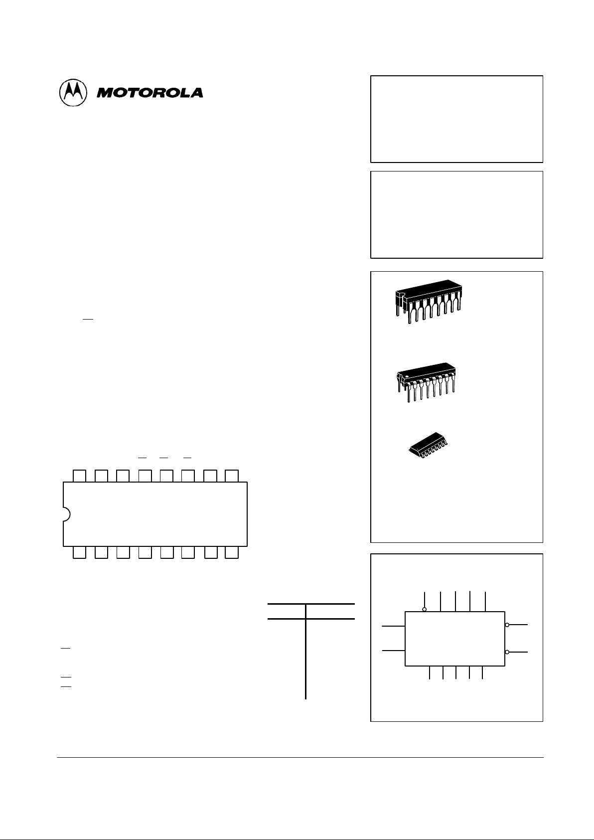
CONNECTION DIAGRAM DIP (TOP VIEW)
14 13 12 11 10 9
123456
7
16 15
8
V
CC
P
1
P0MR TC
DTCU
P
2
PL
P
3
Q1Q0CPDCPUQ2Q3GND
PIN NAMES LOADING (Note a)
HIGH
LOW
CP
U
CP
D
MR
PL
P
n
Q
n
TC
D
TC
U
Count Up Clock Pulse Input
Count Down Clock Pulse Input
Asynchronous Master Reset (Clear) Input
Asynchronous Parallel Load (Active LOW) Input
Parallel Data Inputs
Flip-Flop Outputs (Note b)
Terminal Count Down (Borrow) Output (Note b)
Terminal Count Up (Carry) Output (Note b)
0.5 U.L.
0.5 U.L.
0.5 U.L.
0.5 U.L.
0.5 U.L.
10 U.L.
10 U.L.
10 U.L.
0.25 U.L.
0.25 U.L.
0.25 U.L.
0.25 U.L.
0.25 U.L.
5 (2.5) U.L.
5 (2.5) U.L.
5 (2.5) U.L.
NOTES:
a. 1 TTL Unit Load (U.L.) = 40 µA HIGH/1.6 mA LOW.
b. The Output LOW drive factor is 2.5 U.L. for Military (54) and 5 U.L. for Commercial (74)
b. T emperature Ranges.
SN54/74LS192
SN54/74LS193
PRESETTABLE BCD/DECADE
UP/DOWN COUNTER
PRESETTABLE 4-BIT BINARY
UP/DOWN COUNTER
LOW POWER SCHOTTKY
J SUFFIX
CERAMIC
CASE 620-09
N SUFFIX
PLASTIC
CASE 648-08
16
1
16
1
ORDERING INFORMATION
SN54LSXXXJ Ceramic
SN74LSXXXN Plastic
SN74LSXXXD SOIC
16
1
D SUFFIX
SOIC
CASE 751B-03
LOGIC SYMBOL
VCC = PIN 16
GND = PIN 8
5
4
326
7
12
91011511
CP
D
Q0Q1Q2Q
3
TC
D
P
3
P2P1P
0
PL
CP
U
TC
U
13
MR
14

5-2
FAST AND LS TTL DATA
SN54/74LS192 • SN54/74LS193
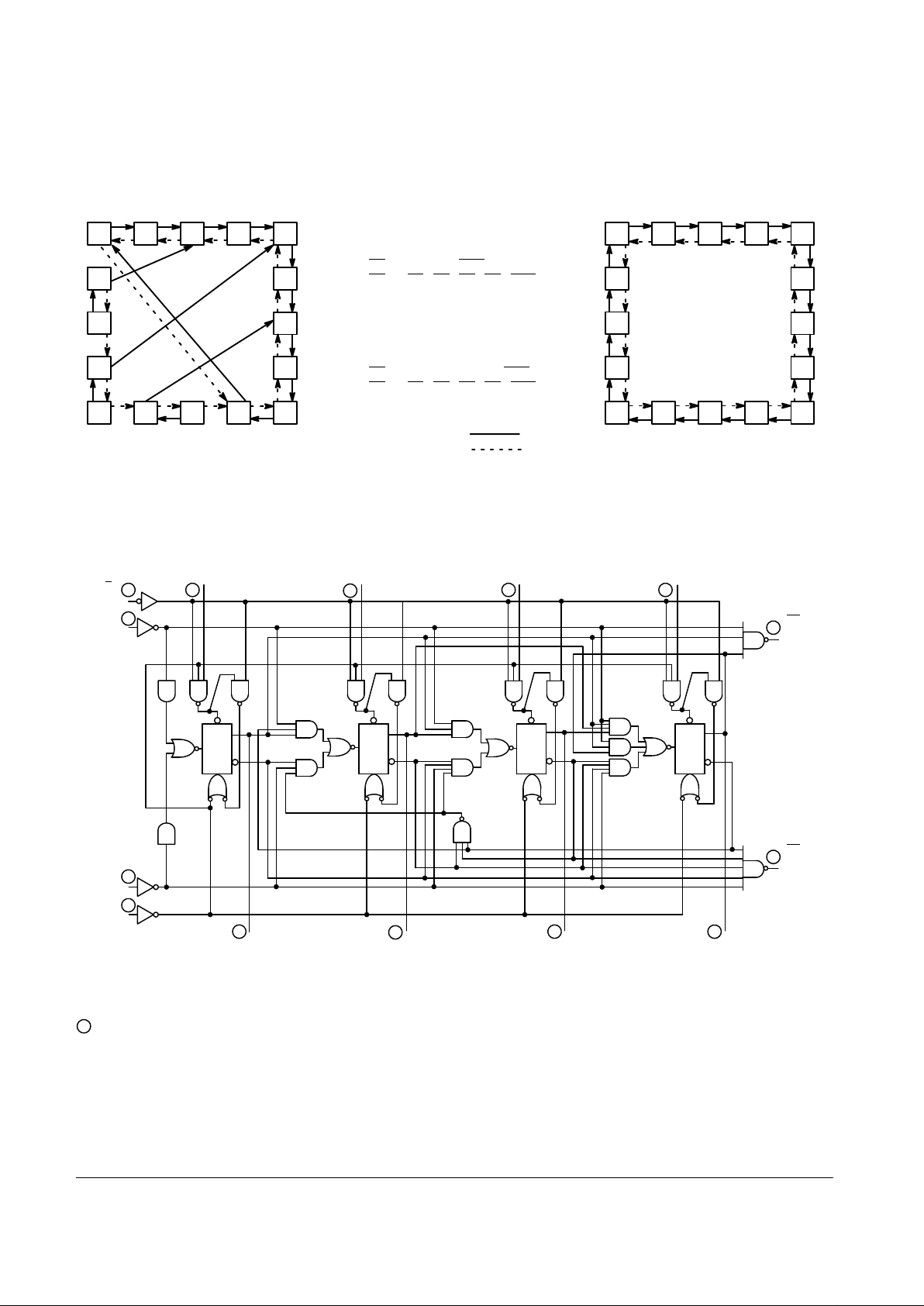
STATE DIAGRAMS
LS192 LOGIC EQUATIONS
FOR TERMINAL COUNT
LS192
LS193
COUNT UP
COUNT DOWN
0123
4
5
6
7
891011
12
13
14
15
0123
4
5
6
7
891011
12
13
14
15
TC
U
= Q0 ⋅ Q3 ⋅ CP
U
TCD = Q0 ⋅ Q1 ⋅ Q2 ⋅ Q3 ⋅ CP
D
LS193 LOGIC EQUATIONS
FOR TERMINAL COUNT
TCU = Q0 ⋅ Q1⋅ Q2⋅ Q3 ⋅ CP
U
TCD = Q0 ⋅ Q1 ⋅ Q2 ⋅ Q3 ⋅ CP
D
LOGIC DIAGRAMS
VCC = PIN 16
GND = PIN 8
= PIN NUMBERS
LS192
P
0
P
1
P
2
P
3
TC
U
(CARRY
OUTPUT)
Q
0
Q
1
Q
2
Q
3
MR
(CLEAR)
(DOWN
COUNT)
CP
D
(UP COUNT)
CP
U
(LOAD)
P
L
1
2
67
3
4
5
911
12
10
13
15
14
TC
D
(BORROW
OUTPUT)
S
D
Q
Q
C
D
T
S
D
Q
Q
C
D
T
S
D
Q
Q
C
D
T
S
D
Q
Q
C
D
T

5-3
FAST AND LS TTL DATA
SN54/74LS192 • SN54/74LS193
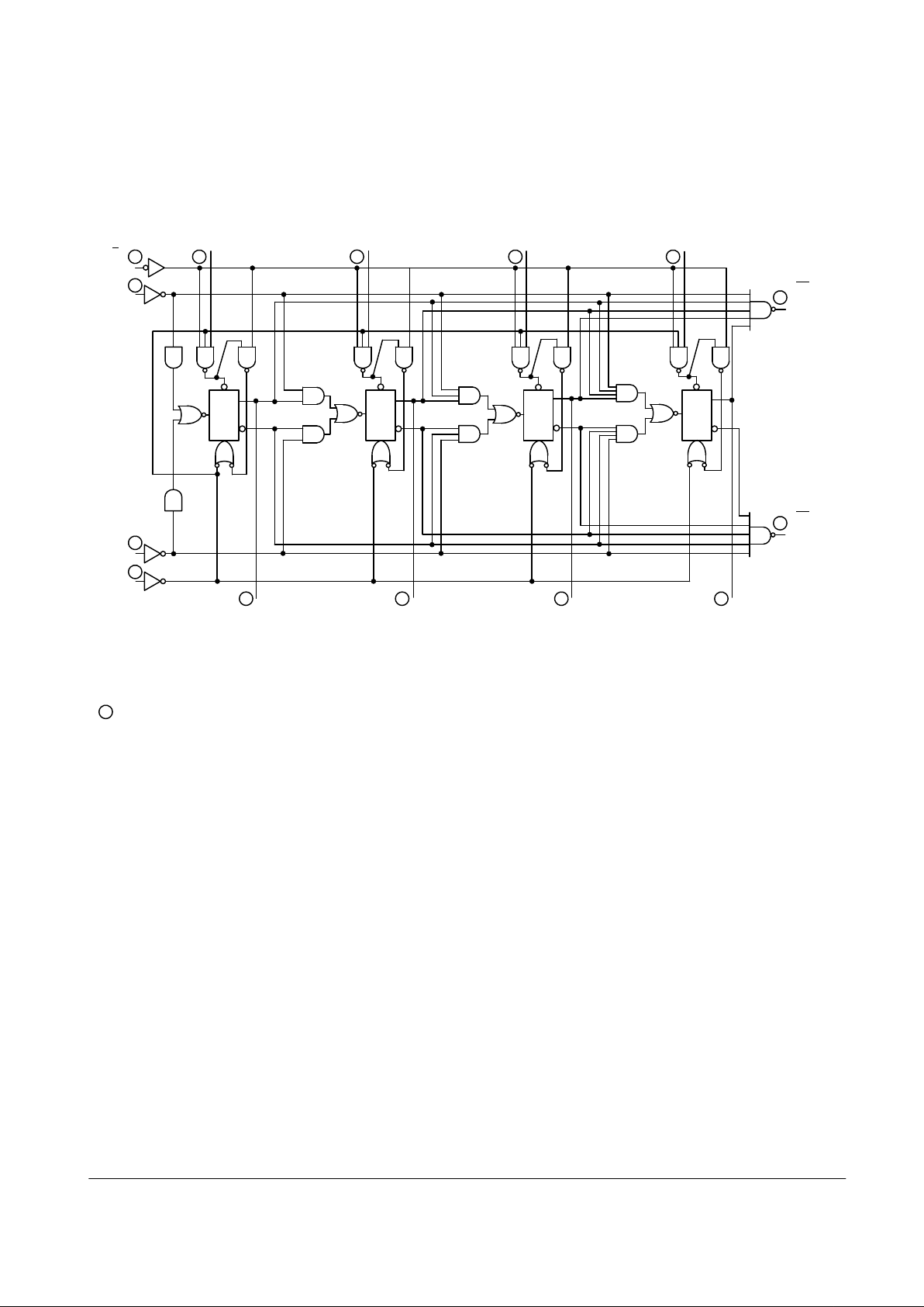
LOGIC DIAGRAMS (continued)
VCC = PIN 16
GND = PIN 8
= PIN NUMBERS
LS193
P
0
P
1
P
2
P
3
Q
0
Q
1
Q
2
Q
3
MR
(CLEAR)
(DOWN
COUNT)
CP
D
(UP COUNT)
CP
U
(LOAD)
P
L
1
2
67
3
4
5
911
12
10
13
15
14
S
D
Q
Q
C
D
T
S
D
Q
Q
C
D
T
S
D
Q
Q
C
D
T
S
D
Q
Q
C
D
T
TC
U
(CARRY
OUTPUT)
TC
D
(BORROW
OUTPUT)
 Loading...