MOTOROLA SN74LS169M, SN74LS169MEL, SN74LS169ML1, SN74LS169N Datasheet

5-1
FAST AND LS TTL DAT A
BCD DECADE/MODULO
16 BINARY SYNCHRONOUS
BI-DIRECTIONAL COUNTERS
The SN54 / 74LS168 and SN54 / 74LS169 are fully synchronous 4-stage
up/down counters featuring a preset capability for programmable operation,
carry lookahead for easy cascading and a U/D input to control the direction
of counting. The SN54/74LS168 counts in a BCD decade (8, 4, 2, 1)
sequence, while the SN54/74LS169 operates in a Modulo 16 binary
sequence. All state changes, whether in counting or parallel loading, are
initiated by the LOW-to-HIGH transition of the clock.
• Low Power Dissipation 100 mW Typical
• High-Speed Count Frequency 30 MHz Typical
• Fully Synchronous Operation
• Full Carry Lookahead for Easy Cascading
• Single Up/Down Control Input
• Positive Edge-Trigger Operation
• Input Clamp Diodes Limit High-Speed Termination Effects
NOTE:
The Flatpak version
has the same pinouts
(Connection Diagram) as
the Dual In-Line Package.
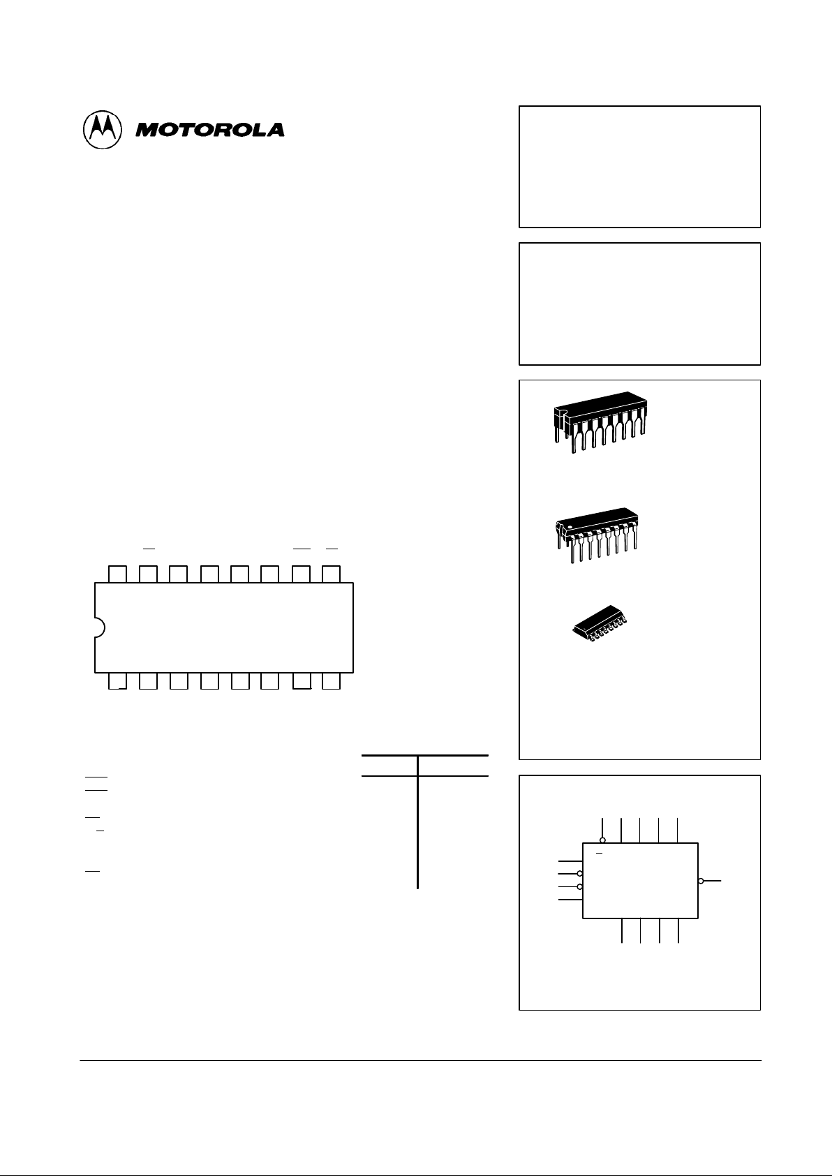
14 13 12 11 10 9
123456
7
16 15
8
V
CC
U/D
TC Q0Q1Q
2
CETQ
3
PE
CP P0P1P2P3CEP GND
CONNECTION DIAGRAM DIP (TOP VIEW)
PIN NAMES LOADING (Note a)
HIGH
LOW
CEP
CET
CP
PE
U/D
P0–P
3
Q0–Q
3
TC
Count Enable Parallel (Active LOW) Input
Count Enable Trickle (Active LOW) Input
Clock Pulse (Active positive going edge) Input
Parallel Enable (Active LOW) Input
Up-Down Count Control Input
Parallel Data Inputs
Flip-Flop Outputs
Terminal Count (Active LOW) Output
0.5 U.L.
1.0 U.L.
0.5 U.L.
0.5 U.L.
0.5 U.L.
0.5 U.L.
10 U.L.
10 U.L.
0.25 U.L.
0.5 U.L.
0.25 U.L.
0.25 U.L.
0.25 U.L.
0.25 U.L.
5 (2.5) U.L.
5 (2.5) U.L.
NOTES:
a. 1 TTL Unit Load (U.L.) = 40 µA HIGH/1.6 mA LOW.
b. The Output LOW drive factor is 2.5 U.L. for Military (54) and 5 U.L. for Commercial (74)
b. T emperature Ranges.
SN54/74LS168
SN54/74LS169
BCD DECADE/MODULO
16 BINARY SYNCHRONOUS
BI-DIRECTIONAL COUNTERS
LOW POWER SCHOTTKY
J SUFFIX
CERAMIC
CASE 620-09
N SUFFIX
PLASTIC
CASE 648-08
16
1
16
1
ORDERING INFORMATION
SN54LSXXXJ Ceramic
SN74LSXXXN Plastic
SN74LSXXXD SOIC
16
1
D SUFFIX
SOIC
CASE 751B-03
LOGIC SYMBOL
934 56
7
10
2
15
14 13 12 11
PE P0P1P2P
3
CEP
CET
CP
Q0Q1Q2Q
3
TC
VCC = PIN 16
GND = PIN 8
1
U/D

5-2
FAST AND LS TTL DATA
SN54/74LS168 • SN54/74LS169
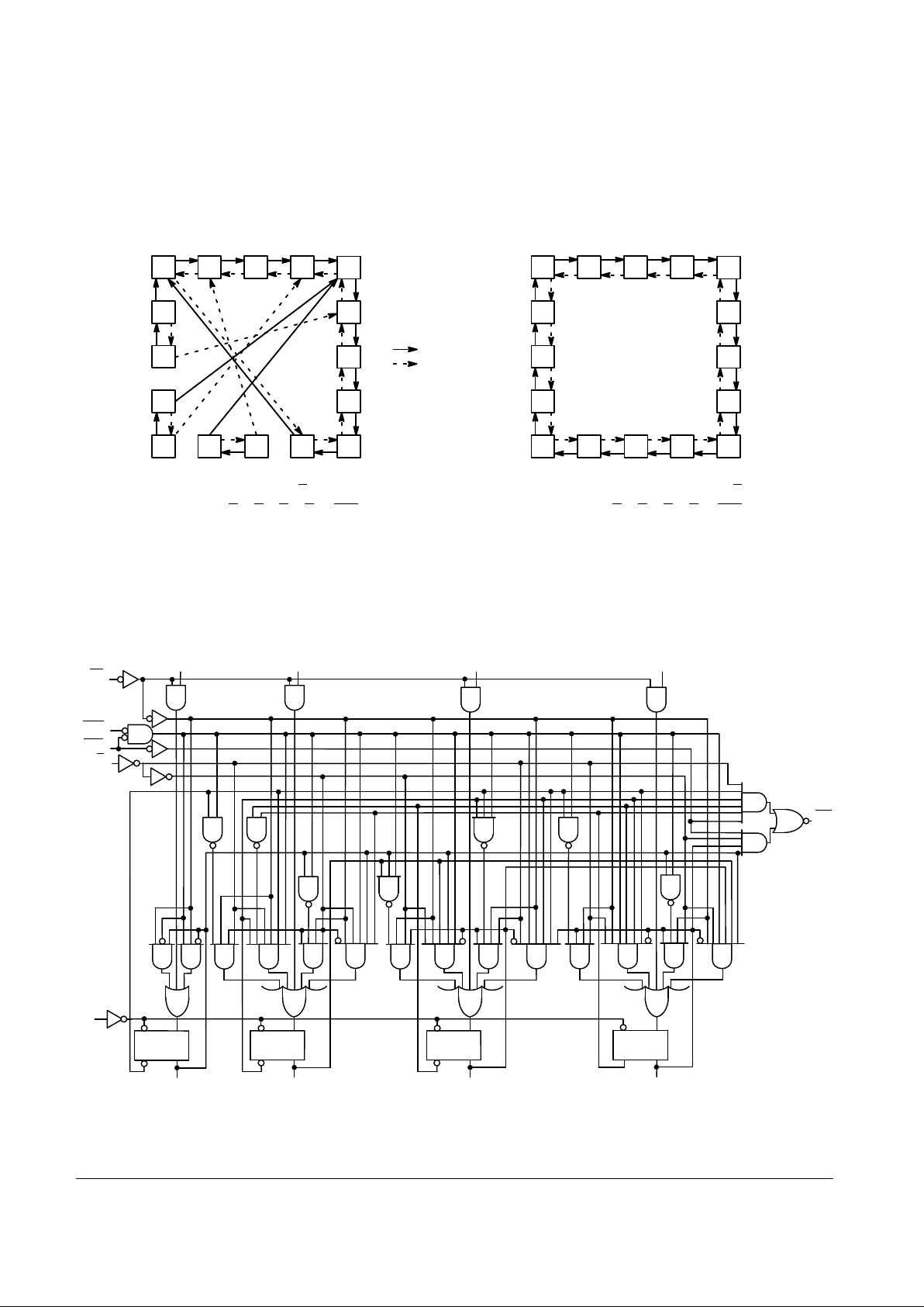
STATE DIAGRAMS
SN54/74LS168
UP/DOWN DECADE COUNTER
0123
4
5
6
7
891011
12
13
14
15
0123
4
5
6
7
891011
12
13
14
15
SN54/74LS169
LOGIC DIAGRAMS
TC
PE
CEP
CET
U/D
CP
P
0
P
1
P
2
P
3
Q
0
Q
1
Q
2
Q
3
CP D
SN54/74LS168
SN54/74LS168
UP: TC = Q0 ⋅ Q3 ⋅ (U/D
)
DOWN: TC = Q
0
⋅ Q1 ⋅ Q2 ⋅ Q3 ⋅ (U/D)
SN54/74LS169
UP: TC = Q0 ⋅ Q1 ⋅ Q2 ⋅ Q3 ⋅ (U/D
)
DOWN: TC = Q
0
⋅ Q1 ⋅ Q2 ⋅ Q3 ⋅ (U/D)
Count Up
Count Down
 Loading...