

MOTOROLA SN74LS161AML1, SN74LS161AML2, SN74LS161AMR1, SN74LS163ADR2, SN74LS163AM Datasheet
...
5-1
FAST AND LS TTL DAT A
BCD DECADE COUNTERS/
4-BIT BINARY COUNTERS
The LS160A/161A/162A/163A are high-speed 4-bit synchronous counters. They are edge-triggered, synchronously presettable, and cascadable
MSI building blocks for counting, memory addressing, frequency division and
other applications. The LS160A and LS162A count modulo 10 (BCD). The
LS161A and LS163A count modulo 16 (binary.)
The LS160A and LS161A have an asynchronous Master Reset (Clear)
input that overrides, and is independent of, the clock and all other control
inputs. The LS162A and LS163A have a Synchronous Reset (Clear) input that
overrides all other control inputs, but is active only during the rising clock
edge.
BCD (Modulo 10) Binary (Modulo 16)
Asynchronous Reset LS160A LS161A
Synchronous Reset LS162A LS163A
• Synchronous Counting and Loading
• Two Count Enable Inputs for High Speed Synchronous Expansion
• Terminal Count Fully Decoded
• Edge-Triggered Operation
• Typical Count Rate of 35 MHz
• ESD > 3500 Volts
CONNECTION DIAGRAM DIP (TOP VIEW)
NOTE:
The Flatpak version
has the same pinouts
(Connection Diagram) as
the Dual In-Line Package.
14 13 12 11 10 9
123456
7
16 15
8
V
CC
*R
TC Q0Q1Q
2
CETQ
3
PE
CP P0P1P2P3CEP GND
*MR for LS160A and LS161A
*SR for LS162A and LS163A
PIN NAMES LOADING (Note a)
HIGH
LOW
PE
P0–P
3
CEP
CET
CP
MR
SR
Q0–Q
3
TC
Parallel Enable (Active LOW) Input
Parallel Inputs
Count Enable Parallel Input
Count Enable Trickle Input
Clock (Active HIGH Going Edge) Input
Master Reset (Active LOW) Input
Synchronous Reset (Active LOW) Input
Parallel Outputs (Note b)
Terminal Count Output (Note b)
1.0 U.L.
0.5 U.L.
0.5 U.L.
1.0 U.L.
0.5 U.L.
0.5 U.L.
1.0 U.L.
10 U.L.
10 U.L.
0.5 U.L.
0.25 U.L.
0.25 U.L.
0.5 U.L.
0.25 U.L.
0.25 U.L.
0.5 U.L.
5 (2.5) U.L.
5 (2.5) U.L.
NOTES:
a) 1 TTL Unit Load (U.L.) = 40 µA HIGH/1.6 mA LOW.
b) The Output LOW drive factor is 2.5 U.L. for Military (54) and 5 U.L. for Commercial (74)
T emperature Ranges.
SN54/74LS160A
SN54/74LS161A
SN54/74LS162A
SN54/74LS163A
BCD DECADE COUNTERS/
4-BIT BINARY COUNTERS
LOW POWER SCHOTTKY
J SUFFIX
CERAMIC
CASE 620-09
N SUFFIX
PLASTIC
CASE 648-08
16
1
16
1
ORDERING INFORMATION
SN54LSXXXJ Ceramic
SN74LSXXXN Plastic
SN74LSXXXD SOIC
16
1
D SUFFIX
SOIC
CASE 751B-03
LOGIC SYMBOL
VCC = PIN 16
GND = PIN 8
93456
7
10
2
15
114131211
PE P0P1P2P
3
CEP
CET
CP
*R Q0Q1Q2Q
3
TC
*MR for LS160A and LS161A
*SR for LS162A and LS163A
*For the LS162A and
*LS163A only.
H = HIGH Voltage Level
L = LOW Voltage Level
X = Don’t Care
5-2
FAST AND LS TTL DATA
SN54/74LS160A • SN54/74LS161A
SN54/74LS162A • SN54/74LS163A
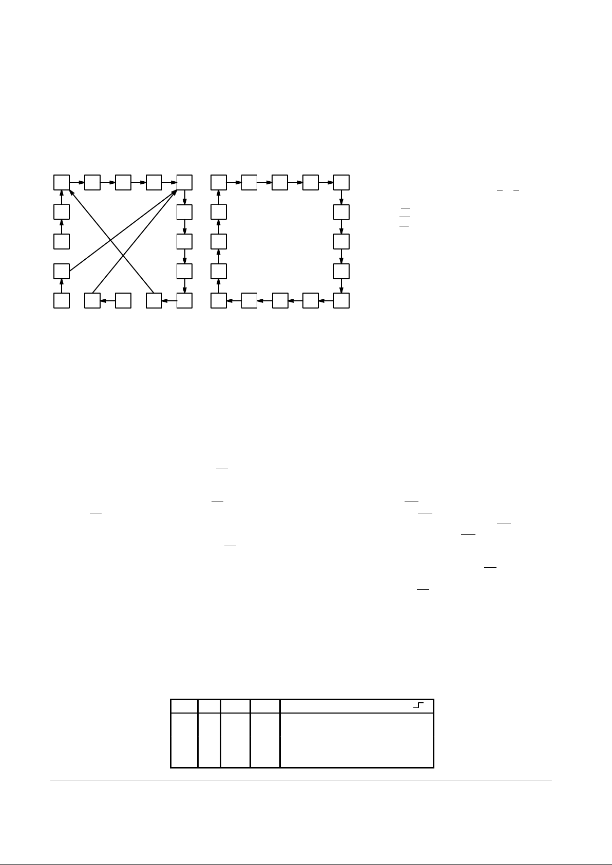
STATE DIAGRAM
LS160A • LS162A LS161A • LS163A
0123
4
5
6
7
891011
12
13
14
15
0123
4
5
6
7
891011
12
13
14
15
NOTE:
The LS160A and LS162A can be preset to any state,
but will not count beyond 9. If preset to state 10, 11,
12, 13, 14, or 15, it will return to its normal sequence
within two clock pulses.
LOGIC EQUATIONS
Count Enable = CEP • CET • PE
TC for LS160A & LS162A = CET • Q0 • Q
1
• Q2 • Q
3
TC for LS161A & LS163A = CET • Q0 • Q1 • Q2 • Q
3
Preset = PE
• CP + (rising clock edge)
Reset = MR
(LS160A & LS161A)
Reset = SR
• CP + (rising clock edge)
Reset = (LS162A & LS163A)
FUNCTIONAL DESCRIPTION
The LS160A/161A/162A/163A are 4-bit synchronous
counters with a synchronous Parallel Enable (Load) feature.
The counters consist of four edge-triggered D flip-flops with
the appropriate data routing networks feeding the D inputs. All
changes of the Q outputs (except due to the asynchronous
Master Reset in the LS160A and LS161A) occur as a result of,
and synchronous with, the LOW to HIGH transition of the
Clock input (CP). As long as the set-up time requirements are
met, there are no special timing or activity constraints on any
of the mode control or data inputs.
Three control inputs — Parallel Enable (PE
), Count Enable
Parallel (CEP) and Count Enable Trickle (CET) — select the
mode of operation as shown in the tables below. The Count
Mode is enabled when the CEP , CET , and PE
inputs are HIGH.
When the PE
is LOW, the counters will synchronously load the
data from the parallel inputs into the flip-flops on the LOW to
HIGH transition of the clock. Either the CEP or CET can be
used to inhibit the count sequence. With the PE
held HIGH, a
LOW on either the CEP or CET inputs at least one set-up time
prior to the LOW to HIGH clock transition will cause the
existing output states to be retained. The AND feature of the
two Count Enable inputs (CET •CEP) allows synchronous
cascading without external gating and without delay accumulation over any practical number of bits or digits.
The Terminal Count (TC) output is HIGH when the Count
Enable Trickle (CET) input is HIGH while the counter is in its
maximum count state (HLLH for the BCD counters, HHHH for
the Binary counters). Note that TC is fully decoded and will,
therefore, be HIGH only for one count state.
The LS160A and LS162A count modulo 10 following a
binary coded decimal (BCD) sequence. They generate a TC
output when the CET input is HIGH while the counter is in state
9 (HLLH). From this state they increment to state 0 (LLLL). If
loaded with a code in excess of 9 they return to their legitimate
sequence within two counts, as explained in the state
diagram. States 10 through 15 do
not
generate a TC output.
The LS161A and LS163A count modulo 16 following a
binary sequence. They generate a TC when the CET input is
HIGH while the counter is in state 15 (HHHH). From this state
they increment to state 0 (LLLL).
The Master Reset (MR
) of the LS160A and LS161A is
asynchronous. When the MR
is LOW, it overrides all other
input conditions and sets the outputs LOW. The MR
pin should
never be left open. If not used, the MR
pin should be tied
through a resistor to VCC, or to a gate output which is
permanently set to a HIGH logic level.
The active LOW Synchronous Reset (SR
) input of the
LS162A and LS163A acts as an edge-triggered control input,
overriding CET, CEP and PE
, and resetting the four counter
flip-flops on the LOW to HIGH transition of the clock. This
simplifies the design from race-free logic controlled reset
circuits, e.g., to reset the counter synchronously after
reaching a predetermined value.
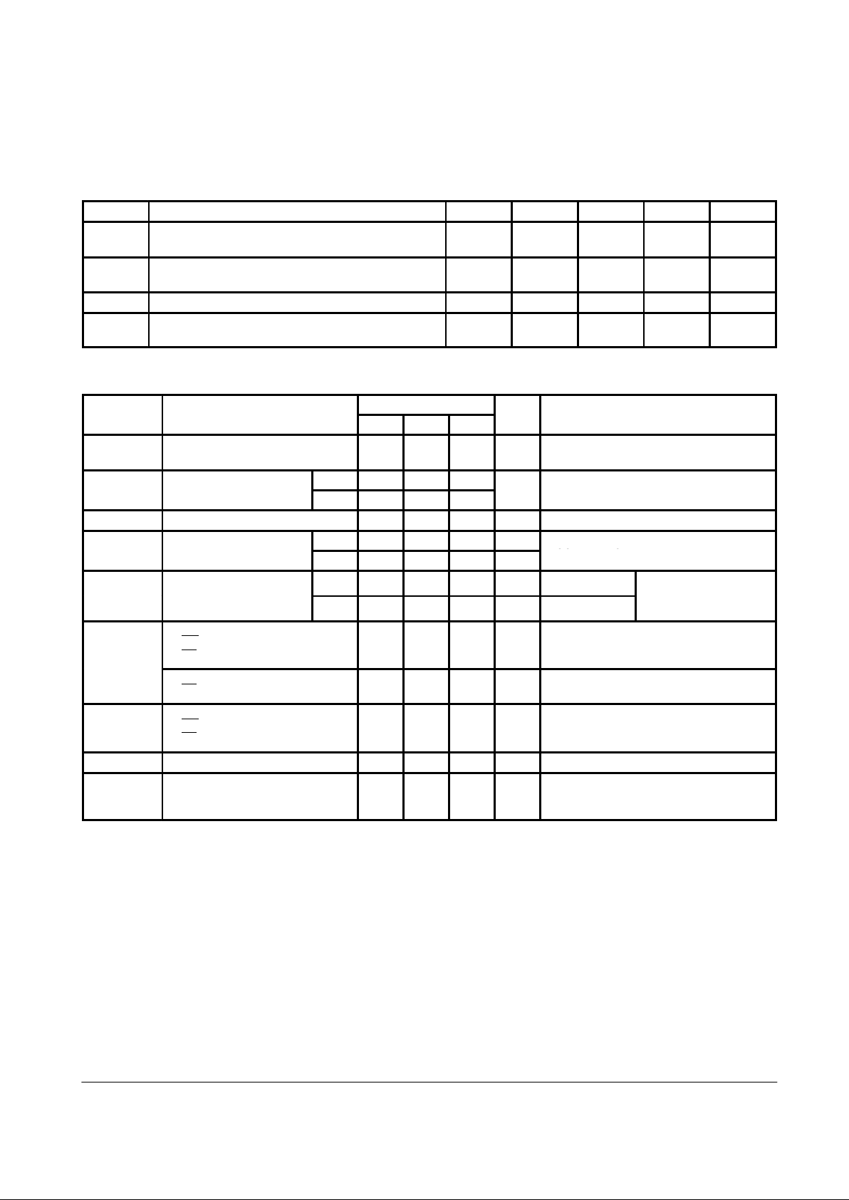
MODE SELECT TABLE
*SR PE CET CEP Action on the Rising Clock Edge ( )
L X X X RESET (Clear)
H L X X LOAD (Pn → Qn)
H H H H COUNT (Increment)
H H L X NO CHANGE (Hold)
H H X L NO CHANGE (Hold)
5-3
FAST AND LS TTL DATA
SN54/74LS160A • SN54/74LS161A
SN54/74LS162A • SN54/74LS163A
GUARANTEED OPERATING RANGES
Symbol Parameter Min Typ Max Unit
V
CC
Supply Voltage 54
74
4.5
4.75
5.0
5.0
5.5
5.25
V
T
A
Operating Ambient Temperature Range 54
74
–55
0
25
25
125
70
°C
I
OH
Output Current — High 54, 74 –0.4 mA
I
OL
Output Current — Low 54
74
4.0
8.0
mA
LS160A and LS161A
DC CHARACTERISTICS OVER OPERATING TEMPERATURE RANGE
(unless otherwise specified)
Limits
Symbol Parameter
Min Typ Max
Unit Test Conditions
V
IH
Input HIGH Voltage 2.0 V
Guaranteed Input HIGH Voltage for
All Inputs
54 0.7
Guaranteed Input LOW Voltage for
VILI
nput
LOW Volt
age
74 0.8
V
pg
All Inputs
V
IK
Input Clamp Diode Voltage –0.65 –1.5 V VCC = MIN, IIN = –18 mA
54 2.5 3.5 V
VCC = MIN, IOH = MAX, VIN = V
IH
VOHOutput HIGH Volt
age
74 2.7 3.5 V
CC
,
OH
,
IN IH
or VIL per Truth Table
54, 74 0.25 0.4 V IOL = 4.0 mA
VCC = VCC MIN,
VOLOutput LOW Volt
age
74 0.35 0.5 V IOL = 8.0 mA
V
IN
=
V
IL
or
V
IH
per Truth Table
I
IH
Input HIGH Current
MR
, Data, CEP, Clock
PE
, CET
20
40
µA VCC = MAX, VIN = 2.7 V
I
IH
MR, Data, CEP, Clock
PE
, CET
0.1
0.2
mA VCC = MAX, VIN = 7.0 V
I
IL
Input LOW Current
MR, Data, CEP, Clock
PE
, CET
–0.4
–0.8
mA VCC = MAX, VIN = 0.4 V
I
OS
Short Circuit Current (Note 1) –20 –100 mA VCC = MAX
I
CC
Power Supply Current
Total, Output HIGH
Total, Output LOW
31
32
mA VCC = MAX
Note 1: Not more than one output should be shorted at a time, nor for more than 1 second.

5-4
FAST AND LS TTL DATA
SN54/74LS160A • SN54/74LS161A
SN54/74LS162A • SN54/74LS163A
LS162A and LS163A
DC CHARACTERISTICS OVER OPERATING TEMPERATURE RANGE
(unless otherwise specified)
Limits
Symbol Parameter
Min Typ Max
Unit Test Conditions
V
IH
Input HIGH Voltage 2.0 V
Guaranteed Input HIGH Voltage for
All Inputs
54 0.7
Guaranteed Input LOW Voltage for
VILI
nput
LOW Volt
age
74 0.8
V
pg
All Inputs
V
IK
Input Clamp Diode Voltage –0.65 –1.5 V VCC = MIN, IIN = –18 mA
54 2.5 3.5 V
VCC = MIN, IOH = MAX, VIN = V
IH
VOHOutput HIGH Volt
age
74 2.7 3.5 V
CC
,
OH
,
IN IH
or VIL per Truth Table
54, 74 0.25 0.4 V IOL = 4.0 mA
VCC = VCC MIN,
VOLOutput LOW Volt
age
74 0.35 0.5 V IOL = 8.0 mA
V
IN
=
V
IL
or
V
IH
per Truth Table
I
IH
Input HIGH Current
Data, CEP, Clock
PE
, CET, SR
20
40
µA VCC = MAX, VIN = 2.7 V
I
IH
Data, CEP, Clock
PE, CET, SR
0.1
0.2
mA VCC = MAX, VIN = 7.0 V
I
IL
Input LOW Current
Data, CEP, Clock, PE
, SR
CET
–0.4
–0.8
mA VCC = MAX, VIN = 0.4 V
I
OS
Short Circuit Current (Note 1) –20 –100 mA VCC = MAX
I
CC
Power Supply Current
Total, Output HIGH
Total, Output LOW
31
32
mA VCC = MAX
Note 1: Not more than one output should be shorted at a time, nor for more than 1 second.
AC CHARACTERISTICS (T
A
= 25°C)
Limits
Symbol Parameter
Min Typ Max
Unit Test Conditions
f
MAX
Maximum Clock Frequency 25 32 MHz
t
PLH
t
PHL
Propagation Delay
Clock to TC
20
18
35
35
ns
t
PLH
t
PHL
Propagation Delay
Clock to Q
13
18
24
27
ns
VCC = 5.0 V
CL = 15 pF
t
PLH
t
PHL
Propagation Delay
CET to TC
9.0
9.0
14
14
ns
t
PHL
MR or SR to Q 20 28 ns

5-5
FAST AND LS TTL DATA
SN54/74LS160A • SN54/74LS161A
SN54/74LS162A • SN54/74LS163A
AC SETUP REQUIREMENTS (T
A
= 25°C)
Limits
Symbol Parameter
Min Typ Max
Unit Test Conditions
tWCP Clock Pulse Width Low 25 ns
t
W
MR or SR Pulse Width 20 ns
t
s
Setup Time, other* 20 ns
t
s
Setup Time PE or SR 25 ns
VCC = 5.0 V
t
h
Hold Time, data 3 ns
t
h
Hold Time, other 0 ns
t
rec
Recovery Time MR to CP 15 ns
*CEP, CET or DAT A
DEFINITION OF TERMS
SETUP TIME (ts) — is defined as the minimum time required
for the correct logic level to be present at the logic input prior to
the clock transition from LOW to HIGH in order to be recognized and transferred to the outputs.
HOLD TIME (th) — is defined as the minimum time following
the clock transition from LOW to HIGH that the logic level must
be maintained at the input in order to ensure continued recog-
nition. A negative HOLD TIME indicates that the correct logic
level may be released prior to the clock transition from LOW to
HIGH and still be recognized.
RECOVERY TIME (t
rec
) — is defined as the minimum time required between the end of the reset pulse and the clock transition from LOW to HIGH in order to recognize and transfer
HIGH Data to the Q outputs.
AC WAVEFORMS
Figure 1. Clock to Output Delays, Count
Frequency, and Clock Pulse Width
Figure 2. Master Reset to Output Delay, Master Reset
Pulse Width, and Master Reset Recovery Time
1.3 V
1.3 V
1.3 V
1.3 V
1.3 V
1.3 V
1.3 V
CP
Q
tW(H) tW(L)
t
rec
t
PHL
t
PHL
t
PLH
OTHER CONDITIONS:
PE
= MR (SR) = H
CEP = CET = H
OTHER CONDITIONS:
PE
= L
P0 = P1 = P2 = P3 = H
t
W
Q0 ⋅ Q1 ⋅ Q2 ⋅ Q
3
MR
CP

5-6
FAST AND LS TTL DATA
SN54/74LS160A • SN54/74LS161A
SN54/74LS162A • SN54/74LS163A
Figure 3
The positive TC pulse occurs when the outputs are in the
(Q0 •Q
1
•Q2 •Q3) state for the LS160 and LS162 and the
(Q0 • Q1 • Q2 • Q3) state for the LS161 and LS163.
OTHER CONDITIONS: CP = PE = CEP = MR = H
1.3 V
t
PHL
t
PLH
1.3 V
1.3 V
1.3 V
CET
TC
AC WAVEFORMS (continued)
The positive TC pulse is coincident with the output state
(Q0 • Q
1
• Q2 • Q3) state for the LS161 and LS163 and
(Q0 • Q1 • Q2 • Q3) for the LS161 and LS163.
Figure 4
OTHER CONDITIONS: PE = CEP = CET = MR = H
1.3 V 1.3 V 1.3 V
1.3 V 1.3 V
t
PLH
t
PHL
CP
TC
The shaded areas indicate when the input is permitted to
change for predictable output performance.
Figure 5
1.3 V1.3 V
OTHER CONDITIONS: PE
= L, MR = H
CP
1.3 V 1.3 V
1.3 V
ts(H)
ts(L)
th(H) = 0
th(L) = 0
Q0
•
Q1 • Q2 • Q
3
P0
•
P1 • P2 • P
3
OTHER CONDITIONS: PE = H, MR = H
1.3 V
1.3 V 1.3 V
1.3 V
1.3 V
1.3 V
1.3 V1.3 V
1.3 V 1.3 V
1.3 V
ts(H)
ts(L)
th(H) = 0 th(L) = 0
ts(H)
th(H) = 0
ts(L)
th(L) = 0
COUNT HOLD HOLD
CEP
CP
CET
Q
CP
SR or PE
Q RESPONSE TO PE
RESET
COUNT OR LOAD
Q RESPONSE TO SR
PARALLEL LOAD
(See Fig. 5)
COUNT MODE
(See Fig. 7)
ts(L)
ts(H)
t
h
(L) = 0
th(H) = 0
1.3 V 1.3 V
Figure 6
COUNT ENABLE TRICKLE INPUT
TO TERMINAL COUNT OUTPUT DELAYS
CLOCK TO TERMINAL COUNT DELAYS
SETUP TIME (ts) AND HOLD TIME (th)
FOR PARALLEL DATA INPUTS
SETUP TIME (ts) AND HOLD TIME (th) FOR
COUNT ENABLE (CEP) AND (CET) AND
PARALLEL ENABLE (PE
) INPUTS
Figure 7
The shaded areas indicate when the input is permitted to
change for predictable output performance.
1.3 V
 Loading...