Motorola MPAA020 Datasheet

SEMICONDUCTOR TECHNICAL DATA
The MPAA020 is a field programmable analog array based on a
general purpose analog cell that may be configured, either alone or in
combinations, as any of a wide range of analog functions from simple
comparators to complex filters. These cells are arranged in a 4 x 5 array
with supporting circuitry to provide input/output signal buffering,
programmable reference voltages, cell to cell interconnections, etc. Each
cell’s function may be programmed to connect with any of the other cells
in the array. Unused cells are powered down individually to minimize power dissipation. Digital interface circuitry is provided to
write the analog circuit configuration data to on–chip SRAM in the same manner as Motorola’s digital FPGAs (serial & parallel
PROM, and microprocessor mode).
Analog circuit design is simplified with EasyAnalog Design Software, which handles bit level circuit configuration details,
allowing the user to do analog design using functional macros in an easy to use point–and–click graphical environment.
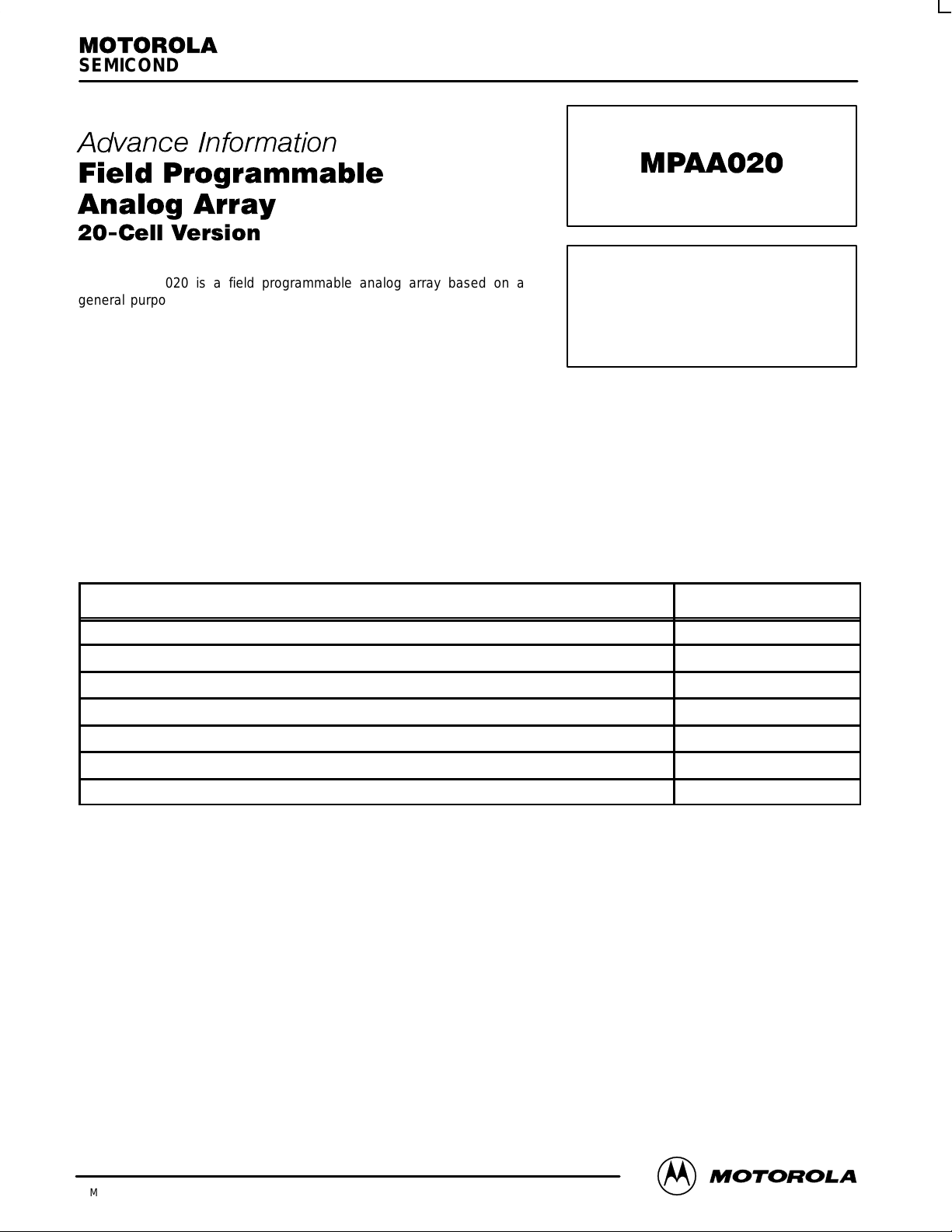
Table 1: Hardware Features
Feature Value
Number of Programmable Cells 20
Analog I/O Cells 13
Anti–aliasing/Smoothing Filtering Sallen–Key External RC
Additional Auxiliary Opamps 8
FIELD PROGRAMMABLE
ANALOG ARRAY
Internal Voltage Reference 8–Bit Programmable
Internal Clock Dividers 4 Independent 5–Bit Dividers
Package 160–Pin QFP
This document contains information on a new product. Specifications and information herein are subject to
change without notice.
4/97
Motorola, Inc. 1997
1
REV 0

MPAA020
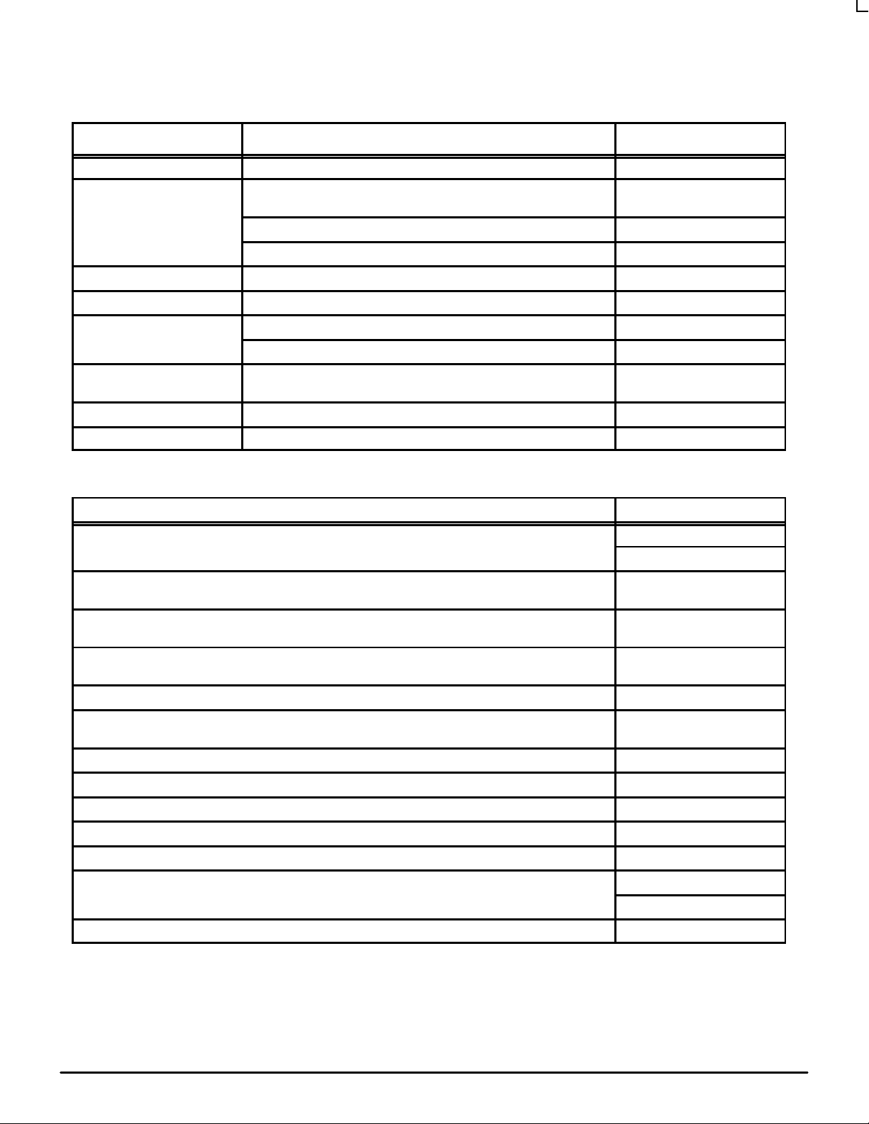
T able 2: EasyAnalog Design Software Macros
Macro Type Definable Parameters Range
Comparator Inverting/Non–inverting Reference level One/Two Input VMR ±2.5 volts
Filters Low Pass/ High Pass/Band Pass/Band Stop Single–Pole/Biquad/Cosine
Filter Pass Band Gain(s)
Q 0.5 to 255
Corner Frequencies Fclk/250 to Fclk/10
Gain Stages Inverting/Noninverting/Summing Offset compensating Gain Value ±(0.004 to 20)
Oscillators Square Wave/Sine Wave Frequency Fclk/1000 to Fclk/4
Rectifiers Full/Half Wave Inverting/Noninverting Gain ±(0.004 to 20)
Low Pass Pole Fclk/250 to Fclk/10
Signal Conditioning Sample–and–Hold
Track–and–Hold
Miscellaneous Differentiator / Integrators / Limiter 0.1 to 2.5 volts
Ramp Generator < 1 Hz to >20 kHz
±(0.004 to 20)
T able 3: Performance Specifications
Specification Typical Value
System Master Clock Frequency (clock) TBD
Internal Sampling Clock Rate 1 MHz (max)
Maximum Signal Frequency – Recommended
– Nyquist
200 kHz
500 kHz
Input Signal Range 0.5 to
Analog Output Drive 100 pF (max)
DC Offset < 10 mV
Harmonic Distortion – 1 kHz
– 200 kHz
Differential Non–Linearity < 0.15 LSB
Integral Non–Linearity < 0.24 LSB
Slew Rate 10 V/usec
Signal to Noise Ratio (SNR) > 60 dB
Power Supply Rejection Ratio (PSRR) TBD
Power Dissipation (max) 200 mW
Each cell individually selectable (10 mW/cell)
Operating Temperature Range –40 to + 85°C
(Vdd – 0.5)
1 kohm (min)
< 0.1%
< 0.5%
MOTOROLA ECLinPS and ECLinPS Lite
2
DL140 — Rev 3

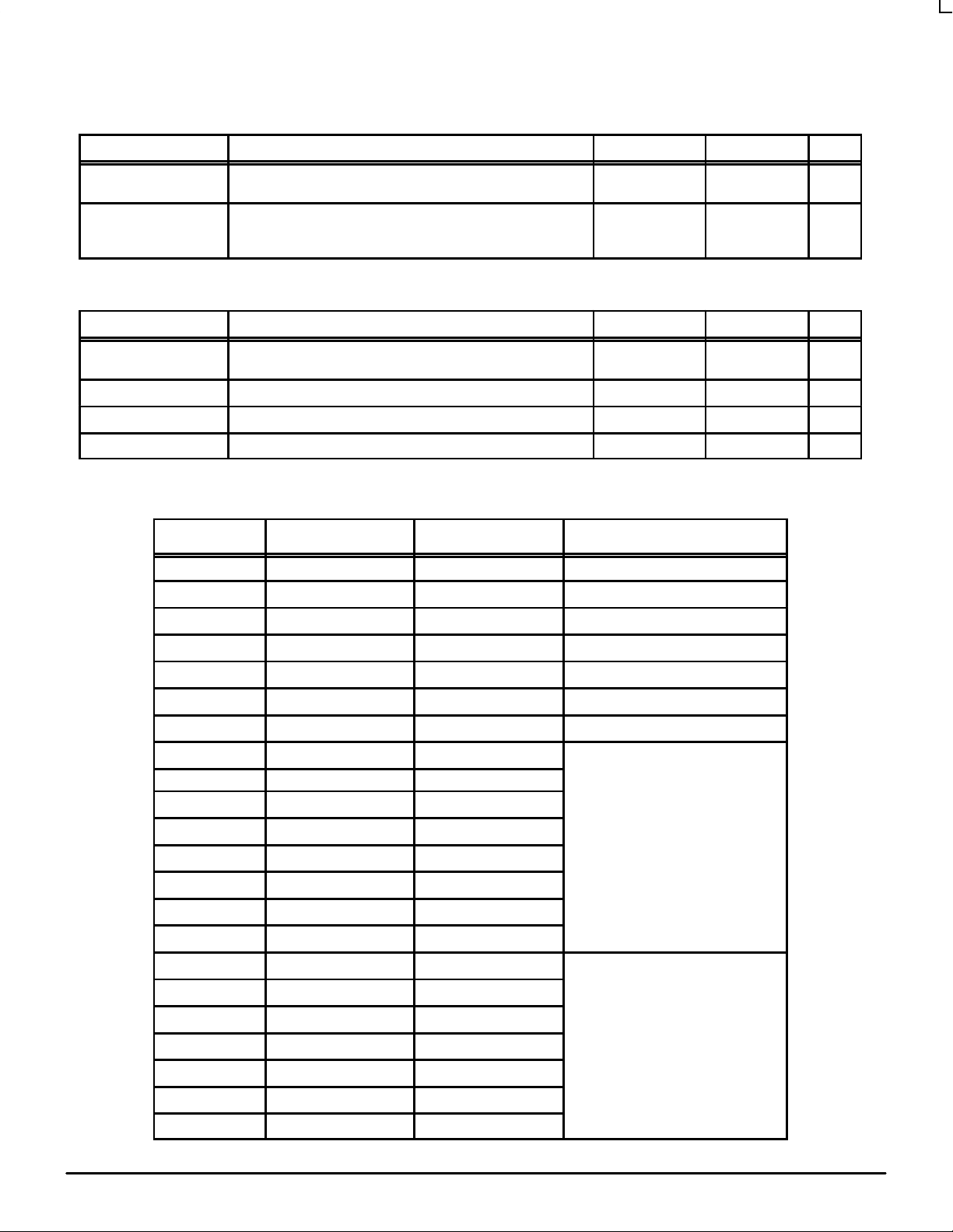
T able 4: Recommended Operating Conditions
Symbol Parameter Min Max Unit
MPAA020
AVDD, BVDD,
DVDD, SVDD
V
in
DC Supply Voltages 4.5 5.5 V
Input Voltage Analog
T able 5: Absolute Maximum Ratings
Symbol Parameter Min Max Unit
AVDD, BVDD,
DVDD, SVDD
V
in
T
A
T
stg
DC Supply Voltages –0.5 6.5 V
Input Voltage –0.5 VDD + 0.5 V
Operating Temperature Range –40 85 C
Storage Temperature –65 150 C
T able 6: Pin Descriptions
Pin Pin Name Type Description
1 por Digital Input Power On Reset
2 mode0 Digital Input Configuration mode control pins
3 mode1 Digital Input
Digital – VOH
Digital – VOL
0.5
2.0
0
VDD – 0.5
DVDD
0.8
V
4 mode2 Digital Input
5 mode3 Digital Input
6 cfg_clk Digital Input External Configuration Clock
7 DClk Digital Output Internal Configuration Clock
8 Data0 Digital Input
9 Data1 Digital Input
10 Data2 Digital Input
11 Data3 Digital Input
12 Data4 Digital Input
13 Data5 Digital Input
14 Data6 Digital Input
15 Data7 Digital Input
16 A0 Digital Output
17 A1 Digital Output
18 A2 Digital Output
19 A3 Digital Output
20 A4 Digital Output
Data Pins Used for Loading
Configuration Data
Address Pins Used for Loading
Configuration Data
DL140 — Rev 3
21 A5 Digital Output
22 A6 Digital Output
3 MOTOROLAECLinPS and ECLinPS Lite
 Loading...