

Motorola MJE16106 Datasheet
1
Motorola Bipolar Power Transistor Device Data
Switchmode Bridge Series
. . . specifically designed for use in half bridge and full bridge off line converters.
• Excellent Dynamic Saturation Characteristics
• Rugged RBSOA Capability
• Collector–Emitter Sustaining Voltage — V
CEO(sus)
— 400 V
• Collector–Emitter Breakdown — V
(BR)CES
— 650 V
• State–of–Art Bipolar Power Transistor Design
• Fast Inductive Switching:
tfi = 30 ns (Typ) @ 100_C
tc = 65 ns (Typ) @ 100_C
tsv = 1.3 µs (Typ) @ 100_C
• Ultrafast FBSOA Specified
• 100_C Performance Specified for:
RBSOA
Inductive Load Switching
Saturation Voltages
Leakages
MAXIMUM RATINGS
Rating
Symbol
Value
Unit
Collector–Emitter Sustaining Voltage
V
CEO(sus)
400
Vdc
Collector–Emitter Breakdown Voltage
V
CES
650
Vdc
Emitter–Base Voltage
V
EBO
6
Vdc
Collector Current — Continuous
— Pulsed (1)
I
C
I
CM
8
16
Adc
Base Current — Continuous
— Pulsed (1)
I
B
I
BM
6
12
Adc
Total Power Dissipation @ TC = 25_C
@ TC = 100_C
Derated above 25_C
P
D
100
40
0.8
Watts
W/_C
Operating and Storage Temperature
TJ, T
stg
–55 to 150
_
C
THERMAL CHARACTERISTICS
Thermal Resistance — Junction to Case
R
θJC
1.25
_
C/W
Maximum Lead Temperature for
Soldering Purposes 1/8″ from
Case for 5 Seconds
T
L
275
_
C
(1) Pulse Test: Pulse Width = 5.0 ms, Duty Cycle v 10%.
Designer’s Data for “Worst Case” Conditions —The Designer’s Data Sheet permits the design of most circuits entirely from the information presented. SOA Limit
curves —representing boundaries on device characteristics —are given to facilitate “worst case” design.
Designer’s and SWITCHMODE are trademarks of Motorola Inc.
SEMICONDUCTOR TECHNICAL DATA
Order this document
by MJE16106/D
Motorola, Inc. 1995
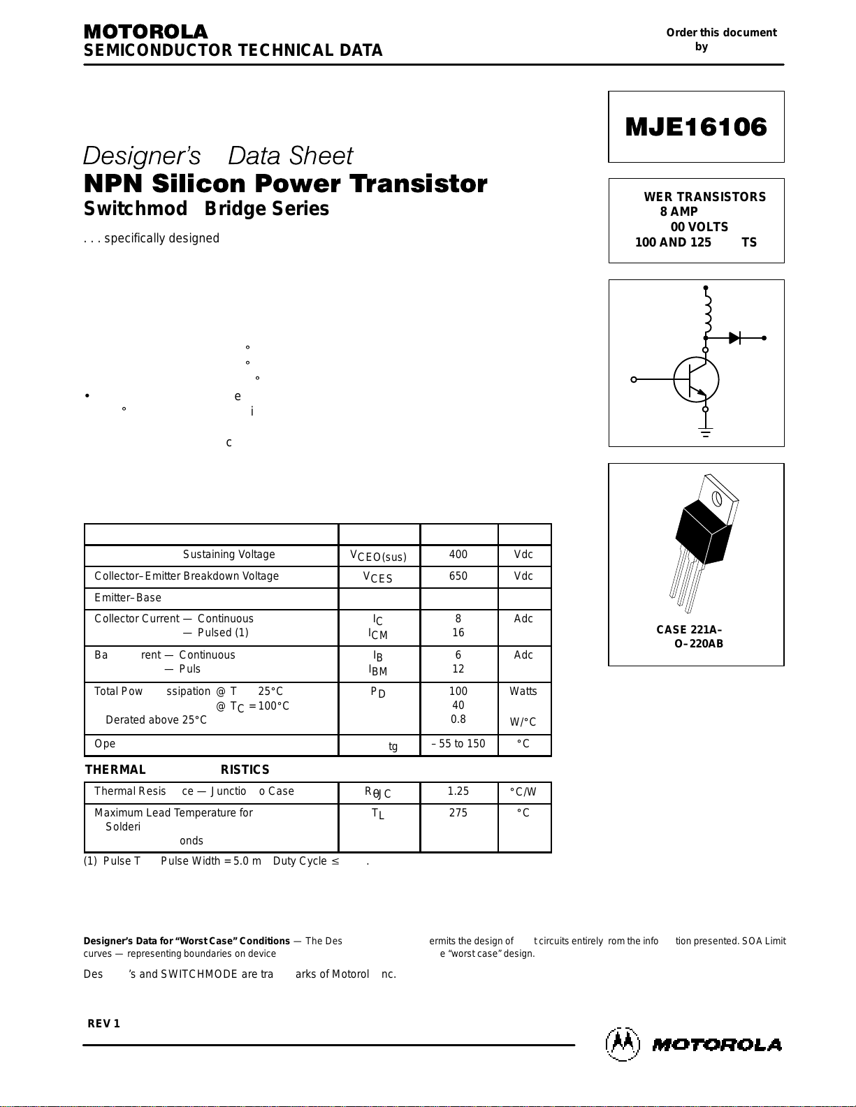
POWER TRANSISTORS
8 AMPERES
400 VOLTS
100 AND 125 WATTS
CASE 221A–06
TO–220AB
REV 1
MJE16106
2
Motorola Bipolar Power Transistor Device Data
ELECTRICAL CHARACTERISTICS (T
C
= 25_C unless otherwise noted)
Characteristic
Symbol
Min
Typ
Max
ÎÎÎ
ÎÎÎ
ÎÎÎ
Unit
OFF CHARACTERISTICS (1)
Collector–Emitter Sustaining Voltage (Table 1)
(IC = 20 mAdc, IB = 0)
V
CEO(sus)
400
—
—
ÎÎÎ
ÎÎÎ
ÎÎÎ
ÎÎÎ
Vdc
Collector Cutoff Current
(VCE = 650 Vdc, V
BE(off)
= 1.5 V)
(VCE = 650 Vdc, V
BE(off)
= 1.5 V, TC = 100_C)
I
CEV
—
—
—
—
100
1000
ÎÎÎ
ÎÎÎ
ÎÎÎ
ÎÎÎ
µAdc
Collector Cutoff Current
(VCE = 650 Vdc, RBE = 50 Ω, TC = 100_C)
I
CER
—
—
1000
ÎÎÎ
ÎÎÎ
ÎÎÎ
ÎÎÎ
µAdc
Emitter–Base Leakage
(VEB = 6.0 Vdc, IC = 0)
I
EBO
—
—
10
ÎÎÎ
ÎÎÎ
ÎÎÎ
ÎÎÎ
µAdc
ON CHARACTERISTICS (1)
Collector–Emitter Saturation Voltage
(IC = 2.5 Adc, IB = 0.25 Adc)
(IC = 5.0 Adc, IB = 0.5 Adc)
(IC = 5.0 Adc, IB = 1.0 Adc)
(IC = 5.0 Adc, IB = 1.0 Adc, TC = 100_C)
V
CE(sat)
—
—
—
—
0.2
0.4
0.2
0.3
0.9
2.0
1.0
1.5
ÎÎÎ
ÎÎÎ
ÎÎÎ
ÎÎÎ
ÎÎÎ
Vdc
Base–Emitter Saturation Voltage
(IC = 5.0 Adc, IB = 1.0 Adc)
(IC = 5.0 Adc, IB = 1.0 Adc, TC = 100_C)
V
BE(sat)
—
—
0.9
0.8
1.5
1.5
ÎÎÎ
ÎÎÎ
ÎÎÎ
ÎÎÎ
ÎÎÎ
Vdc
DC Current Gain
(IC = 8.0 Adc, VCE = 5.0 Vdc)
h
FE
6
13
22
ÎÎÎ
ÎÎÎ
ÎÎÎ
—
DYNAMIC CHARACTERISTICS
Dynamic Saturation
V
CE(dsat)
See Figures 11, 12, and 13
ÎÎÎ
ÎÎÎ
ÎÎÎ
V
Output Capacitance
(VCE = 10 Vdc, IE = 0, f
test
= 1.0 kHz)
C
ob
—
—
300
ÎÎÎ
ÎÎÎ
ÎÎÎ
ÎÎÎ
pF
SWITCHING CHARACTERISTICS
Inductive Load (Table 1)
Storage
t
sv
—
950
2000
ÎÎÎ
ÎÎÎ
ÎÎÎ
Crossover
_
C
t
c
—
45
150
ÎÎÎ
ÎÎÎ
ÎÎÎ
Fall Time
_
C
t
fi
—
20
75
ÎÎÎ
ÎÎÎ
ÎÎÎ
Storage
V
BE(off)
= 5 V,
V
CE(pk)
= 250 V
t
sv
—
1300
2600
ÎÎÎ
ÎÎÎ
ÎÎÎ
Crossover
CE(pk)
= 250 V
_
C
t
c
—
65
200
ÎÎÎ
ÎÎÎ
ÎÎÎ
Fall Time
_
C
t
fi
—
30
125
ÎÎÎ
ÎÎÎ
ÎÎÎ
Resistive Load (Table 2)
Delay Time
t
d
—
30
—
ÎÎÎ
ÎÎÎ
ÎÎÎ
Rise Time
t
r
—
200
—
ÎÎÎ
ÎÎÎ
ÎÎÎ
Storage Time
IC = 5.0 A, IB1 = 0.5 A,
VCC = 250 V,
IB2 = 1.0 A
t
s
—
1800
—
ÎÎÎ
ÎÎÎ
ÎÎÎ
Fall Time
VCC = 250 V,
PW = 30 µs,
t
f
—
100
—
ÎÎÎ
ÎÎÎ
ÎÎÎ
Storage Time
Duty Cycle = v 2.0%
t
s
—
1200
—
ÎÎÎ
ÎÎÎ
ÎÎÎ
Fall Time
v
2.0%
V
BE(off)
= 5 V
t
f
—
70
—
ÎÎÎ
ÎÎÎ
ÎÎÎ
(1) Pulse Test: Pulse Width = 300 µs, Duty Cycle v 2.0%.
IC = 5.0 A, IB1 = 0.5 A,
TJ = 25
TJ = 100
ns
ns
MJE16106
3
Motorola Bipolar Power Transistor Device Data
C, CAPACITANCE (pF)
V
BE
, BASE–EMITTER VOLTAGE (VOLTS)
V
CE
, COLLECTOR–EMITTER VOLTAGE (VOLTS)
V
CE
, COLLECTOR–EMITTER VOLTAGE (VOLTS)
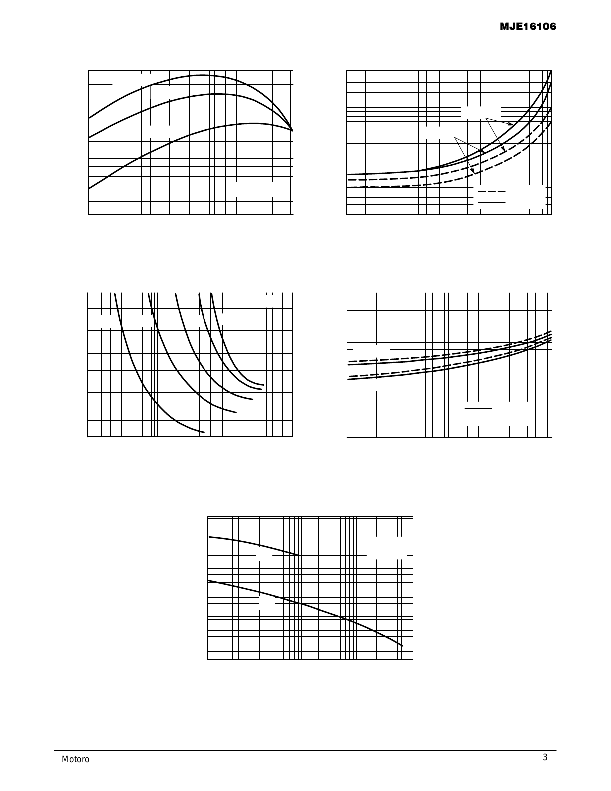
Figure 1. DC Current Gain
IC, COLLECTOR CURRENT (AMPS)
0.05 0.2 2 5
20
h
FE
, DC CURRENT GAIN
0.1 1
2
0.01
0.5
40
30
7
0.02
VCE = 5.0 V
TJ = 100°C
TJ = 25°C
TJ = –55°C
10
IC, COLLECTOR CURRENT (AMPS)
Figure 2. Collector–Emitter Saturation Voltage
0.5
3
0.2
0.03
0.07
1
0.1
0.05
Figure 3. Collector–Emitter Saturation Region
.01
IB, BASE CURRENT (AMPS)
.07.02
1
0.2
0.07
.03 .05 0.1 5
5
0.5
IC = 1 A 3 A
0.2 1 2
5 A
8 A
7 A
3
Figure 4. Base–Emitter Saturation Region
0.1 0.70.2
1.0
0.5
0.2
0.3 0.5 1 10
2.0
0.7
1.5
2 3 5 7
Figure 5. Capacitance
10K
VCE, COLLECTOR–EMITTER VOLTAGE (VOLTS)
C
ib
0.1
5K
2K
1K
500
200
100
50
20
10
0.2 0.5 1 2 5 10 20 50 100 500
300
3K
200
30
1000
TJ = 25°C
f = 1.0 kHz
10
5
3
0.3
2
0.7
0.5 32 50.7 1
0.1 0.2
10
IC/IB = 5
IC/IB = 10
IC, COLLECTOR CURRENT (AMPS)
IC/IB = 10
IC/IB = 5
0.3
7
0.7
0.1
0.05
3
0.3
2
0.3
7K
700
70
0.3 0.50.7 7 10
C
ob
TJ = 100°C
TJ = 25°C
TJ = 25°C
TJ = 25°C
TJ = 100°C
TYPICAL STATIC CHARACTERISTICS
 Loading...