

Motorola MJD117, MJD112 Datasheet
1
Motorola Bipolar Power Transistor Device Data
DPAK For Surface Mount Applications
Designed for general purpose power and switching such as output or driver stages
in applications such as switching regulators, converters, and power amplifiers.
• Lead Formed for Surface Mount Applications in Plastic Sleeves (No Suffix)
• Straight Lead Version in Plastic Sleeves (“1” Suffix)
• Lead Formed Version in 16 mm Tape and Reel (“T4” Suffix)
• Surface Mount Replacements for TIP110–TIP117 Series
• Monolithic Construction With Built–in Base–Emitter Shunt Resistors
• High DC Current Gain — hFE = 2500 (Typ) @ IC = 2.0 Adc
• Complementary Pairs Simplifies Designs
MAXIMUM RATINGS
Rating
Symbol
MJD112
MJD117
Unit
Collector–Emitter Voltage
V
CEO
100
Vdc
Collector–Base Voltage
V
CB
100
Vdc
Emitter–Base Voltage
V
EB
5
Vdc
Collector Current — Continuous
Peak
I
C
2
4
Adc
Base Current
I
B
50
mAdc
Total Power Dissipation @ TC = 25_C
Derate above 25_C
P
D
20
0.16
Watts
W/_C
Total Power Dissipation* @ TA = 25_C
Derate above 25_C
P
D
1.75
0.014
Watts
W/_C
Operating and Storage Junction
Temperature Range
TJ, T
stg
–65 to +150
_
C
THERMAL CHARACTERISTICS
Characteristic
Symbol
Max
Unit
Thermal Resistance, Junction to Case
R
θJC
6.25
_
C/W
Thermal Resistance, Junction to Ambient*
R
θJA
71.4
_
C/W
ELECTRICAL CHARACTERISTICS (T
C
= 25_C unless otherwise noted)
Characteristic
Symbol
Min
Max
Unit
OFF CHARACTERISTICS
Collector–Emitter Sustaining Voltage (1)
(IC = 30 mAdc, IB = 0)
V
CEO(sus)
100
—
Vdc
Collector Cutoff Current
(VCE = 50 Vdc, IB = 0)
I
CEO
—
20
µAdc
Collector Cutoff Current
(VCB = 100 Vdc, IE = 0)
I
CBO
—
20
µAdc
Emitter Cutoff Current
(VBE = 5 Vdc, IC = 0)
I
EBO
—
2
mAdc
*These ratings are applicable when surface mounted on the minimum pad sizes recommended.
(1) Pulse Test: Pulse Width v 300 µs, Duty Cycle v 2%. (continued)
Preferred devices are Motorola recommended choices for future use and best overall value.
SEMICONDUCTOR TECHNICAL DATA
Order this document
by MJD112/D
Motorola, Inc. 1995
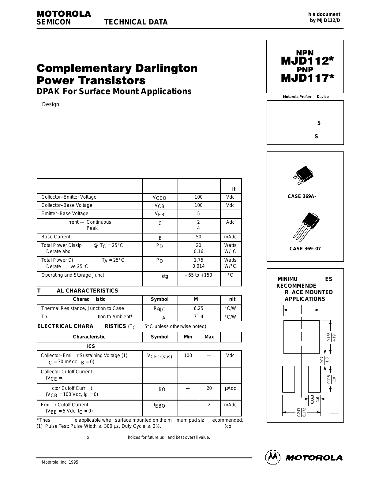
CASE 369A–13
SILICON
POWER TRANSISTORS
2 AMPERES
100 VOLTS
20 WATTS
*Motorola Preferred Device
CASE 369–07
MINIMUM PAD SIZES
RECOMMENDED FOR
SURFACE MOUNTED
APPLICATIONS
0.243
6.172
0.063
1.6
0.118
3.0
0.07
1.8
0.165
4.191
0.190
4.826
inches
mm
REV 1
2
Motorola Bipolar Power Transistor Device Data
*ELECTRICAL CHARACTERISTICS — continued (T
C
= 25_C unless otherwise noted)
Characteristic
ÎÎÎÎ
ÎÎÎÎ
ÎÎÎÎ
Symbol
Min
Max
ÎÎÎ
ÎÎÎ
ÎÎÎ
Unit
OFF CHARACTERISTICS – continued
Collector–Cutoff Current
(VCE = 80 Vdc, V
BE(off)
= 1.5 Vdc)
(VCE = 80 Vdc, V
BE(off)
= 1.5 Vdc, TC = 125_C)
ÎÎÎÎ
ÎÎÎÎ
ÎÎÎÎ
ÎÎÎÎ
ÎÎÎÎ
I
CEX
—
—
10
500
ÎÎÎ
ÎÎÎ
ÎÎÎ
ÎÎÎ
ÎÎÎ
µAdc
Collector–Cutoff Current (VCB = 80 Vdc, IE = 0)
ÎÎÎÎ
ÎÎÎÎ
ÎÎÎÎ
I
CBO
—
10
ÎÎÎ
ÎÎÎ
ÎÎÎ
µAdc
Emitter–Cutoff Current (VBE = 5 Vdc, IC = 0)
ÎÎÎÎ
ÎÎÎÎ
ÎÎÎÎ
I
EBO
—
2
ÎÎÎ
ÎÎÎ
ÎÎÎ
mAdc
ON CHARACTERISTICS
DC Current Gain
(IC = 0.5 Adc, VCE = 3 Vdc)
(IC = 2 Adc, VCE = 3 Vdc)
(IC = 4 Adc, VCE = 3 Vdc)
ÎÎÎÎ
ÎÎÎÎ
ÎÎÎÎ
ÎÎÎÎ
ÎÎÎÎ
h
FE
500
1000
200
—
12,000
—
ÎÎÎ
ÎÎÎ
ÎÎÎ
ÎÎÎ
ÎÎÎ
—
Collector–Emitter Saturation Voltage
(IC = 2 Adc, IB = 8 mAdc)
(IC = 4 Adc, IB = 40 mAdc)
ÎÎÎÎ
ÎÎÎÎ
ÎÎÎÎ
ÎÎÎÎ
ÎÎÎÎ
V
CE(sat)
—
—
2
3
ÎÎÎ
ÎÎÎ
ÎÎÎ
ÎÎÎ
ÎÎÎ
Vdc
Base–Emitter Saturation Voltage (IC = 4 Adc, IB = 40 mAdc)
ÎÎÎÎ
ÎÎÎÎ
ÎÎÎÎ
V
BE(sat)
—
4
ÎÎÎ
ÎÎÎ
ÎÎÎ
Vdc
Base–Emitter On Voltage (IC = 2 Adc, VCE = 3 Vdc)
ÎÎÎÎ
ÎÎÎÎ
ÎÎÎÎ
V
BE(on)
—
2.8
ÎÎÎ
ÎÎÎ
ÎÎÎ
Vdc
DYNAMIC CHARACTERISTICS
Current–Gain — Bandwidth Product
(IC = 0.75 Adc, VCE = 10 Vdc, f = 1 MHz)
ÎÎÎÎ
ÎÎÎÎ
ÎÎÎÎ
f
T
25
—
ÎÎÎ
ÎÎÎ
ÎÎÎ
MHz
Output Capacitance
(VCB = 10 Vdc, IE = 0, f = 0.1 MHz) MJD117
MJD112
ÎÎÎÎ
ÎÎÎÎ
ÎÎÎÎ
ÎÎÎÎ
ÎÎÎÎ
C
ob
—
—
200
100
ÎÎÎ
ÎÎÎ
ÎÎÎ
ÎÎÎ
ÎÎÎ
pF
*Pulse Test: Pulse Width v 300 µs, Duty Cycle v 2%.
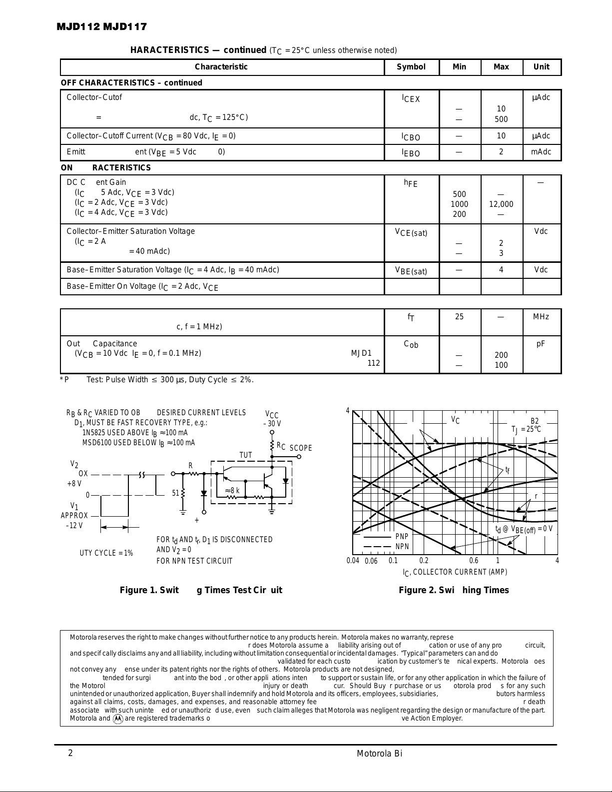
0.04 0.2 40.1
0.06
0.6 1
4
IC, COLLECTOR CURRENT (AMP)
VCC = 30 V
IC/IB = 250
t, TIME ( s)
µ
2
1
0.8
0.6
0.4
0.2
t
s
t
f
Figure 1. Switching Times Test Circuit Figure 2. Switching Times
V
2
APPROX
+8 V
0
≈
8 k
SCOPE
V
CC
–30 V
R
C
51
FOR td AND tr, D1 IS DISCONNECTED
AND V2 = 0
FOR NPN TEST CIRCUIT REVERSE ALL POLARITIES.
25
µ
s
tr, tf
≤
10 ns
DUTY CYCLE = 1%
+ 4 V
t
r
td @ V
BE(off)
= 0 V
PNP
NPN
RB & RC VARIED TO OBTAIN DESIRED CURRENT LEVELS
D1, MUST BE FAST RECOVERY TYPE, e.g.:
1N5825 USED ABOVE IB
≈
100 mA
MSD6100 USED BELOW IB
≈
100 mA
V
1
APPROX
–12 V
TUT
R
B
D
1
≈
60
0.4 2
IB1 = I
B2
TJ = 25
°
C
Motorola reserves the right to make changes without further notice to any products herein. Motorola makes no warranty , representation or guarantee regarding
the suitability of its products for any particular purpose, nor does Motorola assume any liability arising out of the application or use of any product or circuit,
and specifically disclaims any and all liability, including without limitation consequential or incidental damages. “T ypical” parameters can and do vary in different
applications. All operating parameters, including “T ypicals” must be validated for each customer application by customer’s technical experts. Motorola does
not convey any license under its patent rights nor the rights of others. Motorola products are not designed, intended, or authorized for use as components in
systems intended for surgical implant into the body, or other applications intended to support or sustain life, or for any other application in which the failure of
the Motorola product could create a situation where personal injury or death may occur. Should Buyer purchase or use Motorola products for any such
unintended or unauthorized application, Buyer shall indemnify and hold Motorola and its officers, employees, subsidiaries, affiliates, and distributors harmless
against all claims, costs, damages, and expenses, and reasonable attorney fees arising out of, directly or indirectly, any claim of personal injury or death
associated with such unintended or unauthorized use, even if such claim alleges that Motorola was negligent regarding the design or manufacture of the part.
Motorola and are registered trademarks of Motorola, Inc. Motorola, Inc. is an Equal Opportunity/Affirmative Action Employer.
 Loading...