

Motorola MC74HC162AD, MC74HC162AN, MC74HC160AD, MC74HC160AN, MC54HC162AJ Datasheet
...
SEMICONDUCTOR TECHNICAL DATA
1
REV 0
Motorola, Inc. 1996
9/96
High–Performance Silicon–Gate CMOS
The MC54/74HC160A and HC162A are identical in pinout to the LS160
and LS162, respectively. The device inputs are compatible with standard
CMOS outputs; with pullup resistors, they are compatible with LSTTL
outputs.
The HC160A and HC162A are programmable BCD counters with
asynchronous and synchronous Reset inputs, respectively.
• Output Drive Capability: 10 LSTTL Loads
• Outputs Directly Interface to CMOS, NMOS, and TTL
• Operating Voltage Range: 2 to 6 V
• Low Input Current: 1 µA
• High Noise Immunity Characteristic of CMOS Devices
• In Compliance with the Requirements Defined by JEDEC Standard
No. 7A
• Chip Complexity: 234 FETs or 58.5 Equivalent Gates
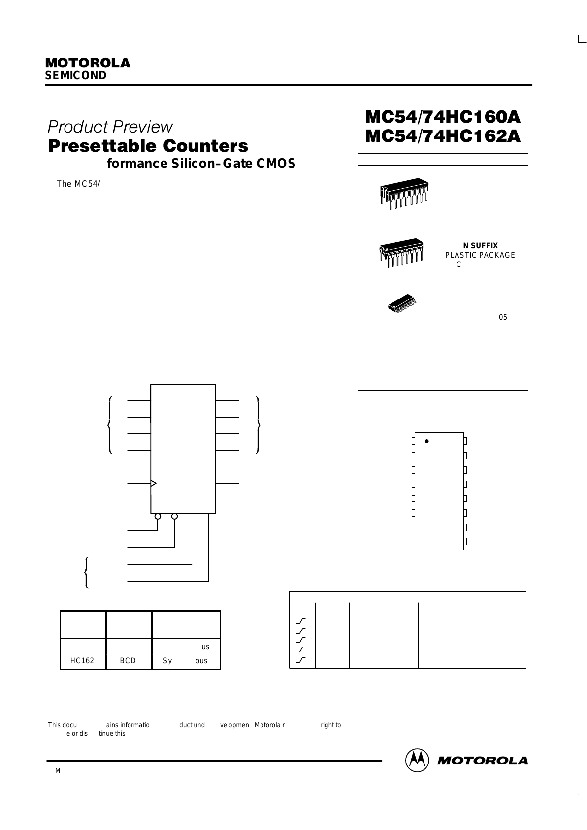
LOGIC DIAGRAM
PIN 16 = V
CC
PIN 8 = GND
11
12
13
14
Q0
Q1
Q2
Q3
15
RIPPLE
CARRY
OUT
BCD
OUTPUTS
3
4
5
6
P0
P1
P2
P3
2
CLOCK
RESET
LOAD
ENABLE P
ENABLE T
COUNT
ENABLES
PRESENT
DATA
INPUTS
ÎÎÎ
Î
Device
ÎÎ
Î
Count
Mode
ÎÎÎÎ
Reset Mode
HC160
BCD
Asynchronous
HC162
BCD
Synchronous
This document contains information on a product under development. Motorola reserves the right to
change or discontinue this product without notice.
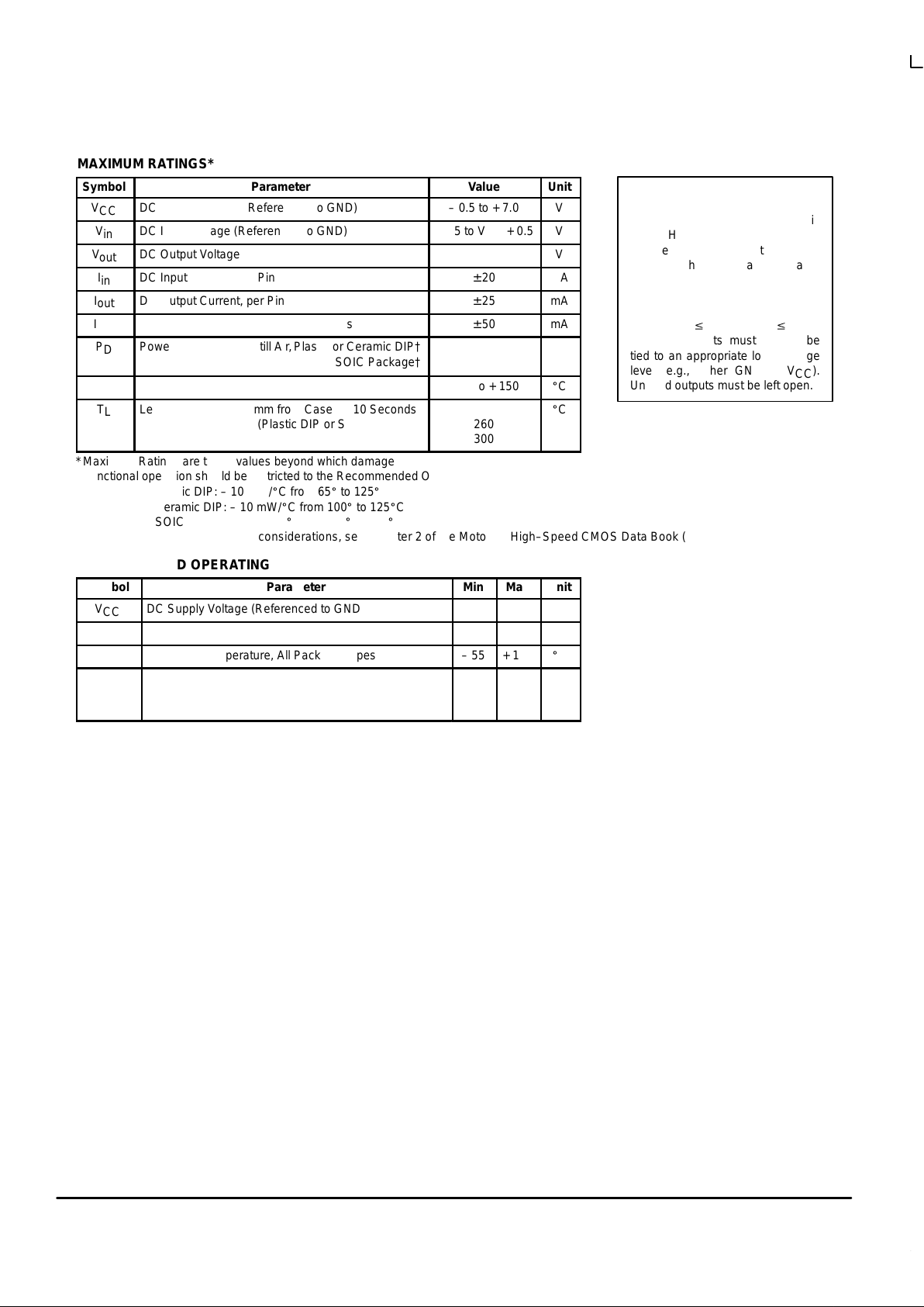
PIN ASSIGNMENT
13
14
15
16
9
10
11
12
5
4
3
2
1
8
7
6
RESET
P0
CLOCK
GND
Q1
Q0
RIPPLE
CARRY OUT
V
CC
P1
P2
P3
ENABLE P
Q2
Q3
ENABLE T
LOAD
D SUFFIX
SOIC PACKAGE
CASE 751B–05
N SUFFIX
PLASTIC PACKAGE
CASE 648–08
ORDERING INFORMATION
MC54HCXXXAJ
MC74HCXXXAN
MC74HCXXXAD
Ceramic
Plastic
SOIC
1
16
1
16
J SUFFIX
CERAMIC PACKAGE
CASE 620–10
1
16
Inputs Output
Clock Reset* Load Enable P Enable T Q
L X X X Reset
H L X X Load Preset Data
H H H H Count
H H L X No Count
H H X L No Count
FUNCTION TABLE
*HC162A only. HC160A is an Asynchronous Reset Device
H = high level
L = low level
X = don’t care
MC54/74HC160A MC54/74HC162A
MOTOROLA High–Speed CMOS Logic Data
DL129 — Rev 6
2
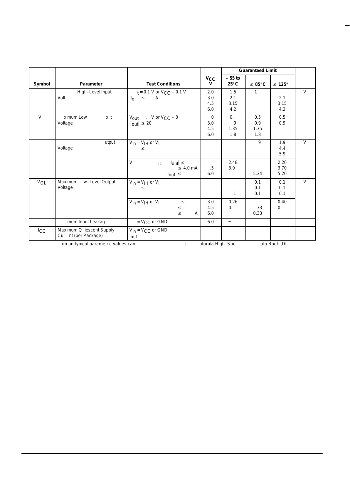
MAXIMUM RATINGS*
Symbol
Parameter
Value
Unit
V
CC
DC Supply Voltage (Referenced to GND)
– 0.5 to + 7.0
V
V
in
DC Input Voltage (Referenced to GND)
– 0.5 to VCC + 0.5
V
V
out
DC Output Voltage (Referenced to GND)
– 0.5 to VCC + 0.5
V
I
in
DC Input Current, per Pin
± 20
mA
I
out
DC Output Current, per Pin
± 25
mA
I
CC
DC Supply Current, VCC and GND Pins
± 50
mA
Î
Î
P
D
ОООООООООООО
Î
Power Dissipation in Still Air,Plastic or Ceramic DIP†
SOIC Package†
ÎÎÎÎ
Î
750
500
Î
Î
mW
T
stg
Storage Temperature
– 65 to + 150
_
C
Î
Î
T
L
ОООООООООООО
Î
Lead Temperature, 1 mm from Case for 10 Seconds
(Plastic DIP or SOIC Package)
(Ceramic DIP)
ÎÎÎÎ
Î
260
300
Î
Î
_
C
*Maximum Ratings are those values beyond which damage to the device may occur.
Functional operation should be restricted to the Recommended Operating Conditions.
†Derating — Plastic DIP: – 10 mW/_C from 65_ to 125_C
Ceramic DIP: – 10 mW/_C from 100_ to 125_C
SOIC Package: – 7 mW/_C from 65_ to 125_C
For high frequency or heavy load considerations, see Chapter 2 of the Motorola High–Speed CMOS Data Book (DL129/D).
RECOMMENDED OPERATING CONDITIONS
Symbol
Parameter
Min
Max
Unit
V
CC
DC Supply Voltage (Referenced to GND)
2.0
6.0
V
Vin, V
out
DC Input Voltage, Output Voltage (Referenced to GND)
0
V
CC
V
T
A
Operating Temperature, All Package Types
– 55
+ 125
_
C
ÎÎ
Î
ÎÎ
Î
tr, t
f
ОООООООООООО
Î
ОООООООООООО
Î
Input Rise and Fall Time VCC = 2.0 V
(Figure 1) VCC = 4.5 V
VCC = 6.0 V
Î
Î
Î
Î
0
0
0
Î
Î
Î
Î
1000
500
400
Î
Î
Î
Î
ns
This device contains protection
circuitry to guard against damage
due to high static voltages or electric
fields. However, precautions must
be taken to avoid applications of any
voltage higher than maximum rated
voltages to this high–impedance circuit. For proper operation, Vin and
V
out
should be constrained to the
range GND v (Vin or V
out
) v VCC.
Unused inputs must always be
tied to an appropriate logic voltage
level (e.g., either GND or VCC).
Unused outputs must be left open.
MC54/74HC160A MC54/74HC162A
High–Speed CMOS Logic Data
DL129 — Rev 6
3 MOTOROLA
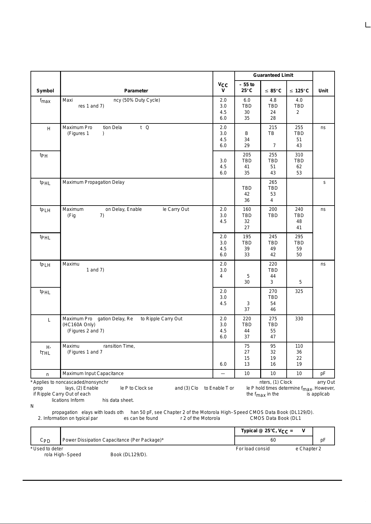
DC ELECTRICAL CHARACTERISTICS (Voltages Referenced to GND)
Guaranteed Limit
ÎÎ
Î
Symbol
ООООООО
Î
Parameter
ООООООО
Î
Test Conditions
ÎÎ
Î
V
CC
V
ÎÎ
– 55 to
25_C
ÎÎ
Î
v
85_C
ÎÎ
Î
v
125_C
Î
Î
Unit
ÎÎ
Î
ÎÎ
V
IH
ООООООО
Î
ООООООО
Minimum High–Level Input
Voltage
ООООООО
Î
ООООООО
V
out
= 0.1 V or VCC – 0.1 V
|I
out
| v 20 µA
ÎÎ
Î
ÎÎ
2.0
3.0
4.5
6.0
ÎÎ
ÎÎ
1.5
2.1
3.15
4.2
ÎÎ
Î
ÎÎ
1.5
2.1
3.15
4.2
ÎÎ
Î
ÎÎ
1.5
2.1
3.15
4.2
Î
Î
Î
V
ÎÎ
Î
ÎÎ
Î
V
IL
ООООООО
Î
ООООООО
Î
Maximum Low–Level Input
Voltage
ООООООО
Î
ООООООО
Î
V
out
= 0.1 V or VCC – 0.1 V
|I
out
| v 20 µA
ÎÎ
Î
ÎÎ
Î
2.0
3.0
4.5
6.0
ÎÎ
ÎÎ
0.5
0.9
1.35
1.8
ÎÎ
Î
ÎÎ
Î
0.5
0.9
1.35
1.8
ÎÎ
Î
ÎÎ
Î
0.5
0.9
1.35
1.8
Î
Î
Î
Î
V
ÎÎ
Î
ÎÎ
Î
V
OH
ООООООО
Î
ООООООО
Î
Minimum High–Level Output
Voltage
ООООООО
Î
ООООООО
Î
Vin = VIH or V
IL
|I
out
| v 20 µA
ÎÎ
Î
ÎÎ
Î
2.0
4.5
6.0
ÎÎ
ÎÎ
1.9
4.4
5.9
ÎÎ
Î
ÎÎ
Î
1.9
4.4
5.9
ÎÎ
Î
ÎÎ
Î
1.9
4.4
5.9
Î
Î
Î
Î
V
ÎÎÎОООООООÎООООООО
Î
Vin = VIH or VIL|I
out
| v 2.4 m
|I
out
| v 4.0 mA
|I
out
| v 5.2 mA
ÎÎ
Î
3.0
4.5
6.0
ÎÎ
2.48
3.98
5.48
ÎÎ
Î
2.34
3.84
5.34
ÎÎ
Î
2.20
3.70
5.20
Î
Î
ÎÎ
Î
V
OL
ООООООО
Î
Maximum Low–Level Output
Voltage
ООООООО
Î
Vin = VIH or V
IL
|I
out
| v 20 µA
ÎÎ
Î
2.0
4.5
6.0
ÎÎ
0.1
0.1
0.1
ÎÎ
Î
0.1
0.1
0.1
ÎÎ
Î
0.1
0.1
0.1
Î
Î
V
ÎÎÎОООООООÎООООООО
Î
Vin = VIH or VIL|I
out
| v 2.4 m
|I
out
| v 4.0 mA
|I
out
| v 5.2 mA
ÎÎ
Î
3.0
4.5
6.0
ÎÎ
0.26
0.26
0.26
ÎÎ
Î
0.33
0.33
0.33
ÎÎ
Î
0.40
0.40
0.40
Î
Î
I
in
Maximum Input Leakage Current
Vin = VCC or GND
6.0
± 0.1
± 1.0
± 1.0
µA
ÎÎ
Î
I
CC
ООООООО
Î
Maximum Quiescent Supply
Current (per Package)
ООООООО
Î
Vin = VCC or GND
I
out
= 0 µA
ÎÎ
Î
6.0
ÎÎ4ÎÎ
Î
40
ÎÎ
Î
160
Î
Î
µA
NOTE:Information on typical parametric values can be found in Chapter 2 of the Motorola High–Speed CMOS Data Book (DL129/D).
MC54/74HC160A MC54/74HC162A
MOTOROLA High–Speed CMOS Logic Data
DL129 — Rev 6
4
AC ELECTRICAL CHARACTERISTICS (C
L
= 50 pF, Input tr = tf = 6 ns)
Guaranteed Limit
ÎÎ
Î
Symbol
ООООООООООООООО
Î
Parameter
ÎÎ
Î
V
CC
V
ÎÎ
– 55 to
25_C
ÎÎ
Î
v
85_C
ÎÎ
Î
v
125_C
Î
Î
Unit
ÎÎ
Î
ÎÎ
Î
f
max
ООООООООООООООО
Î
ООООООООООООООО
Î
Maximum Clock Frequency (50% Duty Cycle)*
(Figures 1 and 7)
ÎÎ
Î
ÎÎ
Î
2.0
3.0
4.5
6.0
ÎÎ
ÎÎ
6.0
TBD
30
35
ÎÎ
Î
ÎÎ
Î
4.8
TBD
24
28
ÎÎ
Î
ÎÎ
Î
4.0
TBD
20
24
Î
Î
Î
Î
MHz
ÎÎ
Î
ÎÎ
Î
t
PLH
ООООООООООООООО
Î
ООООООООООООООО
Î
Maximum Propagation Delay, Clock to Q
(Figures 1 and 7)
ÎÎ
Î
ÎÎ
Î
2.0
3.0
4.5
6.0
ÎÎ
ÎÎ
170
TBD
34
29
ÎÎ
Î
ÎÎ
Î
215
TBD
43
37
ÎÎ
Î
ÎÎ
Î
255
TBD
51
43
Î
Î
Î
Î
ns
ÎÎ
Î
ÎÎ
Î
t
PHL
ООООООООООООООО
Î
ООООООООООООООО
Î
ÎÎ
Î
ÎÎ
Î
2.0
3.0
4.5
6.0
ÎÎ
ÎÎ
205
TBD
41
35
ÎÎ
Î
ÎÎ
Î
255
TBD
51
43
ÎÎ
Î
ÎÎ
Î
310
TBD
62
53
Î
Î
Î
Î
ÎÎ
Î
ÎÎ
Î
t
PHL
ООООООООООООООО
Î
ООООООООООООООО
Î
Maximum Propagation Delay, Reset to Q (HC160A Only)
(Figures 2 and 7)
ÎÎ
Î
ÎÎ
Î
2.0
3.0
4.5
6.0
ÎÎ
ÎÎ
210
TBD
42
36
ÎÎ
Î
ÎÎ
Î
265
TBD
53
45
ÎÎ
Î
ÎÎ
Î
315
TBD
63
54
Î
Î
Î
Î
ns
ÎÎ
Î
ÎÎ
Î
t
PLH
ООООООООООООООО
Î
ООООООООООООООО
Î
Maximum Propagation Delay, Enable T to Ripple Carry Out
(Figures 3 and 7)
ÎÎ
Î
ÎÎ
Î
2.0
3.0
4.5
6.0
ÎÎ
ÎÎ
160
TBD
32
27
ÎÎ
Î
ÎÎ
Î
200
TBD
40
34
ÎÎ
Î
ÎÎ
Î
240
TBD
48
41
Î
Î
Î
Î
ns
ÎÎ
Î
ÎÎ
Î
ÎÎ
Î
t
PHL
ООООООООООООООО
Î
ООООООООООООООО
Î
ООООООООООООООО
Î
ÎÎ
Î
ÎÎ
Î
ÎÎ
Î
2.0
3.0
4.5
6.0
ÎÎ
ÎÎ
ÎÎ
195
TBD
39
33
ÎÎ
Î
ÎÎ
Î
ÎÎ
Î
245
TBD
49
42
ÎÎ
Î
ÎÎ
Î
ÎÎ
Î
295
TBD
59
50
Î
Î
Î
Î
Î
Î
ÎÎ
Î
ÎÎ
Î
ÎÎ
t
PLH
ООООООООООООООО
Î
ООООООООООООООО
Î
ООООООООООООООО
Maximum Propagation Delay, Clock to Ripple Carry Out
(Figures 1 and 7)
ÎÎ
Î
ÎÎ
Î
ÎÎ
2.0
3.0
4.5
6.0
ÎÎ
ÎÎ
ÎÎ
175
TBD
35
30
ÎÎ
Î
ÎÎ
Î
ÎÎ
220
TBD
44
37
ÎÎ
Î
ÎÎ
Î
ÎÎ
265
TBD
53
45
Î
Î
Î
Î
Î
ns
ÎÎ
Î
ÎÎ
Î
t
PHL
ООООООООООООООО
Î
ООООООООООООООО
Î
ÎÎ
Î
ÎÎ
Î
2.0
3.0
4.5
6.0
ÎÎ
ÎÎ
215
TBD
43
37
ÎÎ
Î
ÎÎ
Î
270
TBD
54
46
ÎÎ
Î
ÎÎ
Î
325
TBD
65
55
Î
Î
Î
Î
ÎÎ
Î
ÎÎ
Î
t
PHL
ООООООООООООООО
Î
ООООООООООООООО
Î
Maximum Propagation Delay, Reset to Ripple Carry Out
(HC160A Only)
(Figures 2 and 7)
ÎÎ
Î
ÎÎ
Î
2.0
3.0
4.5
6.0
ÎÎ
ÎÎ
220
TBD
44
37
ÎÎ
Î
ÎÎ
Î
275
TBD
55
47
ÎÎ
Î
ÎÎ
Î
330
TBD
66
56
Î
Î
Î
Î
ns
ÎÎ
Î
ÎÎ
Î
t
TLH
,
t
THL
ООООООООООООООО
Î
ООООООООООООООО
Î
Maximum Output Transition Time, Any Output
(Figures 1 and 7)
ÎÎ
Î
ÎÎ
Î
2.0
3.0
4.5
6.0
ÎÎ
ÎÎ
75
27
15
13
ÎÎ
Î
ÎÎ
Î
95
32
19
16
ÎÎ
Î
ÎÎ
Î
110
36
22
19
Î
Î
Î
Î
ns
C
in
Maximum Input Capacitance
—
10
10
10
pF
*Applies to noncascaded/nonsynchronously clocked configurations only. With synchronously cascaded counters, (1) Clock to Ripple Carry Out
propagation delays, (2) Enable T or Enable P to Clock setup times, and (3) Clock to Enable T or Enable P hold times determine f
max
. However,
if Ripple Carry Out of each stage is tied to the Clock of the next stage (nonsynchronously clocked), the f
max
in the table above is applicable.
See Applications Information in this data sheet.
NOTES:
1. For propagation delays with loads other than 50 pF, see Chapter 2 of the Motorola High–Speed CMOS Data Book (DL129/D).
2. Information on typical parametric values can be found in Chapter 2 of the Motorola High–Speed CMOS Data Book (DL129/D).
Typical @ 25°C, VCC = 5.0 V
C
PD
Power Dissipation Capacitance (Per Package)*
60
pF
*Used to determine the no–load dynamic power consumption: PD = CPD V
CC
2
f + ICC VCC. For load considerations, see Chapter 2 of the
Motorola High–Speed CMOS Data Book (DL129/D).
MC54/74HC160A MC54/74HC162A
High–Speed CMOS Logic Data
DL129 — Rev 6
5 MOTOROLA
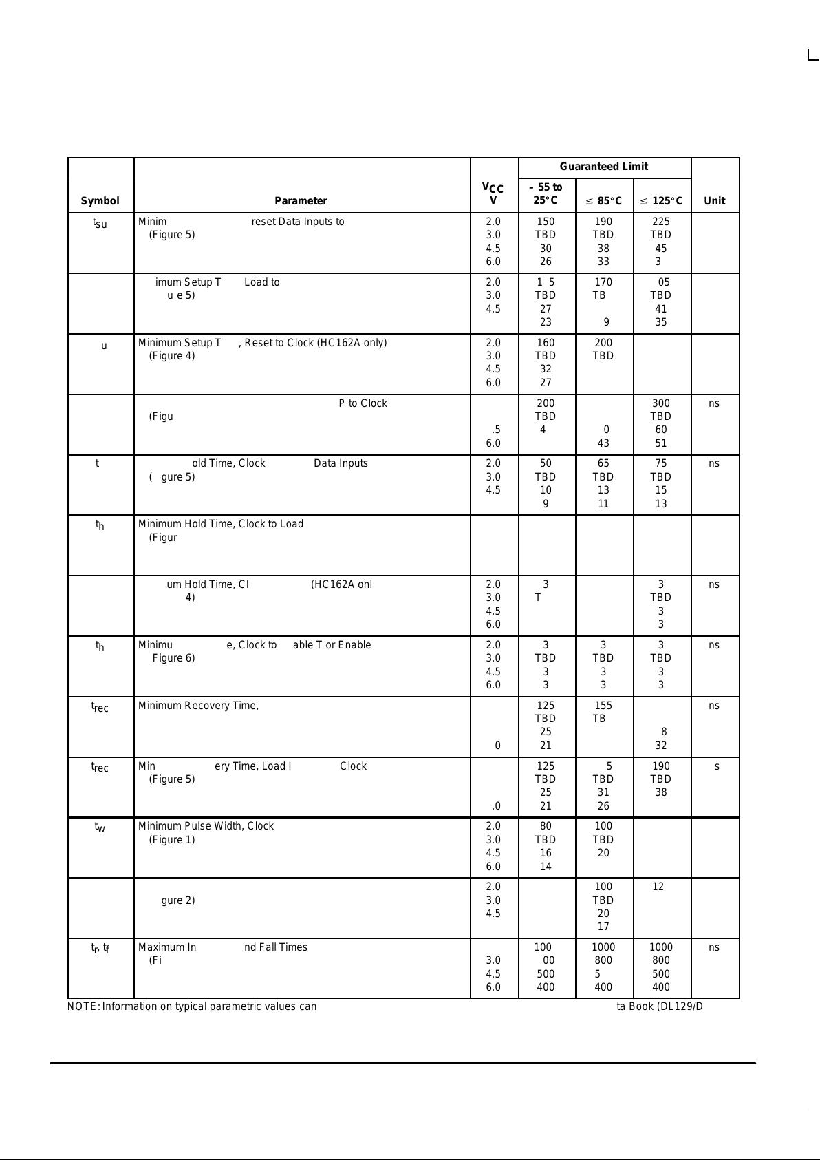
TIMING REQUIREMENTS (Input t
r
= tf = 6 ns)
Guaranteed Limit
ÎÎ
Î
Symbol
ООООООООООООООО
Î
Parameter
ÎÎ
Î
V
CC
V
ÎÎ
– 55 to
25_C
ÎÎ
Î
v
85_C
ÎÎ
Î
v
125_C
Î
Î
Unit
ÎÎ
Î
ÎÎ
Î
t
su
ООООООООООООООО
Î
ООООООООООООООО
Î
Minimum Setup Time, Preset Data Inputs to Clock
(Figure 5)
ÎÎ
Î
ÎÎ
Î
2.0
3.0
4.5
6.0
ÎÎ
ÎÎ
150
TBD
30
26
ÎÎ
Î
ÎÎ
Î
190
TBD
38
33
ÎÎ
Î
ÎÎ
Î
225
TBD
45
38
Î
Î
Î
Î
ns
ÎÎ
Î
ÎÎ
Î
t
su
ООООООООООООООО
Î
ООООООООООООООО
Î
Minimum Setup Time, Load to Clock
(Figure 5)
ÎÎ
Î
ÎÎ
Î
2.0
3.0
4.5
6.0
ÎÎ
ÎÎ
135
TBD
27
23
ÎÎ
Î
ÎÎ
Î
170
TBD
34
29
ÎÎ
Î
ÎÎ
Î
205
TBD
41
35
Î
Î
Î
Î
ns
ÎÎ
Î
ÎÎ
Î
t
su
ООООООООООООООО
Î
ООООООООООООООО
Î
Minimum Setup Time, Reset to Clock (HC162A only)
(Figure 4)
ÎÎ
Î
ÎÎ
Î
2.0
3.0
4.5
6.0
ÎÎ
ÎÎ
160
TBD
32
27
ÎÎ
Î
ÎÎ
Î
200
TBD
40
34
ÎÎ
Î
ÎÎ
Î
240
TBD
48
41
Î
Î
Î
Î
ns
ÎÎ
Î
ÎÎ
Î
t
su
ООООООООООООООО
Î
ООООООООООООООО
Î
Minimum Setup Time, Enable T or Enable P to Clock
(Figure 6)
ÎÎ
Î
ÎÎ
Î
2.0
3.0
4.5
6.0
ÎÎ
ÎÎ
200
TBD
40
34
ÎÎ
Î
ÎÎ
Î
250
TBD
50
43
ÎÎ
Î
ÎÎ
Î
300
TBD
60
51
Î
Î
Î
Î
ns
ÎÎ
Î
ÎÎ
Î
t
h
ООООООООООООООО
Î
ООООООООООООООО
Î
Minimum Hold Time, Clock to Preset Data Inputs
(Figure 5)
ÎÎ
Î
ÎÎ
Î
2.0
3.0
4.5
6.0
ÎÎ
ÎÎ
50
TBD
10
9
ÎÎ
Î
ÎÎ
Î
65
TBD
13
11
ÎÎ
Î
ÎÎ
Î
75
TBD
15
13
Î
Î
Î
Î
ns
ÎÎ
Î
ÎÎ
Î
ÎÎ
t
h
ООООООООООООООО
Î
ООООООООООООООО
Î
ООООООООООООООО
Minimum Hold Time, Clock to Load
(Figure 5)
ÎÎ
Î
ÎÎ
Î
ÎÎ
2.0
3.0
4.5
6.0
ÎÎ
ÎÎ
ÎÎ
3
TBD
3
3
ÎÎ
Î
ÎÎ
Î
ÎÎ
3
TBD
3
3
ÎÎ
Î
ÎÎ
Î
ÎÎ
3
TBD
3
3
Î
Î
Î
Î
Î
ns
ÎÎ
Î
ÎÎ
Î
t
h
ООООООООООООООО
Î
ООООООООООООООО
Î
Minimum Hold Time, Clock to Reset (HC162A only)
(Figure 4)
ÎÎ
Î
ÎÎ
Î
2.0
3.0
4.5
6.0
ÎÎ
ÎÎ
3
TBD
3
3
ÎÎ
Î
ÎÎ
Î
3
TBD
3
3
ÎÎ
Î
ÎÎ
Î
3
TBD
3
3
Î
Î
Î
Î
ns
ÎÎ
Î
ÎÎ
Î
t
h
ООООООООООООООО
Î
ООООООООООООООО
Î
Minimum Hold Time, Clock to Enable T or Enable P
(Figure 6)
ÎÎ
Î
ÎÎ
Î
2.0
3.0
4.5
6.0
ÎÎ
ÎÎ
3
TBD
3
3
ÎÎ
Î
ÎÎ
Î
3
TBD
3
3
ÎÎ
Î
ÎÎ
Î
3
TBD
3
3
Î
Î
Î
Î
ns
ÎÎ
Î
ÎÎ
Î
t
rec
ООООООООООООООО
Î
ООООООООООООООО
Î
Minimum Recovery Time, Reset Inactive to Clock (HC160A only)
(Figure 2)
ÎÎ
Î
ÎÎ
Î
2.0
3.0
4.5
6.0
ÎÎ
ÎÎ
125
TBD
25
21
ÎÎ
Î
ÎÎ
Î
155
TBD
31
26
ÎÎ
Î
ÎÎ
Î
190
TBD
38
32
Î
Î
Î
Î
ns
ÎÎ
Î
ÎÎ
Î
t
rec
ООООООООООООООО
Î
ООООООООООООООО
Î
Minimum Recovery Time, Load Inactive to Clock
(Figure 5)
ÎÎ
Î
ÎÎ
Î
2.0
3.0
4.5
6.0
ÎÎ
ÎÎ
125
TBD
25
21
ÎÎ
Î
ÎÎ
Î
155
TBD
31
26
ÎÎ
Î
ÎÎ
Î
190
TBD
38
32
Î
Î
Î
Î
ns
ÎÎ
Î
ÎÎ
Î
t
w
ООООООООООООООО
Î
ООООООООООООООО
Î
Minimum Pulse Width, Clock
(Figure 1)
ÎÎ
Î
ÎÎ
Î
2.0
3.0
4.5
6.0
ÎÎ
ÎÎ
80
TBD
16
14
ÎÎ
Î
ÎÎ
Î
100
TBD
20
17
ÎÎ
Î
ÎÎ
Î
120
TBD
24
20
Î
Î
Î
Î
ns
ÎÎ
Î
ÎÎ
Î
t
w
ООООООООООООООО
Î
ООООООООООООООО
Î
Minimum Pulse Width, Reset (HC160A only)
(Figure 2)
ÎÎ
Î
ÎÎ
Î
2.0
3.0
4.5
6.0
ÎÎ
ÎÎ
80
TBD
16
14
ÎÎ
Î
ÎÎ
Î
100
TBD
20
17
ÎÎ
Î
ÎÎ
Î
120
TBD
24
20
Î
Î
Î
Î
ns
ÎÎ
Î
ÎÎ
Î
tr, t
f
ООООООООООООООО
Î
ООООООООООООООО
Î
Maximum Input Rise and Fall Times
(Figure 1)
ÎÎ
Î
ÎÎ
Î
2.0
3.0
4.5
6.0
ÎÎ
ÎÎ
1000
800
500
400
ÎÎ
Î
ÎÎ
Î
1000
800
500
400
ÎÎ
Î
ÎÎ
Î
1000
800
500
400
Î
Î
Î
Î
ns
NOTE:Information on typical parametric values can be found in Chapter 2 of the Motorola High–Speed CMOS Data Book (DL129/D).
 Loading...