

MOTOROLA MC74HC161AFR2, MC74HC161AN, MC74HC161AFR1, MC74HC163AD, MC74HC163ADR2 Datasheet
...
Semiconductor Components Industries, LLC, 2000
March, 2000 – Rev. 8
1 Publication Order Number:
MC74HC161A/D
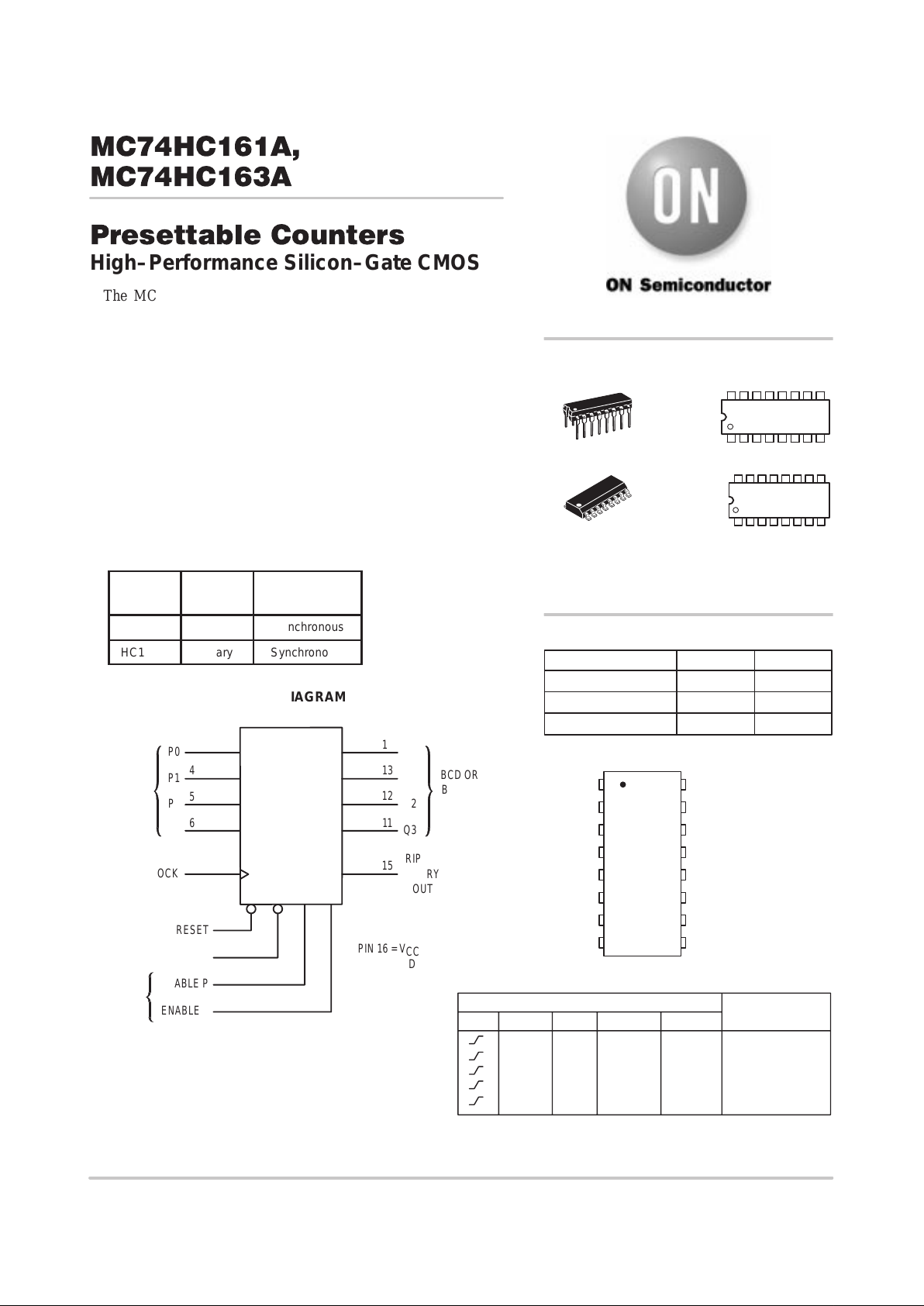
MC74HC161A,
MC74HC163A
Presettable Counters
High–Performance Silicon–Gate CMOS
The MC74HC161A and HC163A are identical in pinout to the
LS161 and LS163. The device inputs are compatible with standard
CMOS outputs; with pullup resistors, they are compatible with
LSTTL outputs.
The HC161A and HC163A are programmable 4–bit binary counters
with asynchronous and synchronous reset, respectively.
• Output Drive Capability: 10 LSTTL Loads
• Outputs Directly Interface to CMOS, NMOS, and TTL
• Operating Voltage Range: 2.0 to 6.0 V
• Low Input Current: 1.0 µA
• High Noise Immunity Characteristic of CMOS Devices
• In Compliance with the Requirements Defined by JEDEC Standard
No. 7A
• Chip Complexity: 192 FETs or 48 Equivalent Gates
ÎÎ
Î
Device
ÎÎ
Î
Count
Mode
ÎÎÎÎ
Î
Reset Mode
HC161A
Binary
Asynchronous
HC163A
Binary
Synchronous
LOGIC DIAGRAM
PIN 16 = V
CC
PIN 8 = GND
11
12
13
14
Q0
Q1
Q2
Q3
15
RIPPLE
CARRY
OUT
BCD OR
BINARY
OUTPUT
3
4
5
6
P0
P1
P2
P3
2
CLOCK
RESET
LOAD
ENABLE P
ENABLE T
COUNT
ENABLES
PRESET
DATA
INPUTS
1
9
7
10
Inputs Output
Clock Reset* Load Enable P Enable T Q
L X X X Reset
H L X X Load Preset Data
H H H H Count
H H L X No Count
H H X L No Count
FUNCTION TABLE
*HC163A only. HC161A is an Asynchronous Reset Device
H = high level, L = low level, X = don’t care
PIN ASSIGNMENT
13
14
15
16
9
10
11
125
4
3
2
1
8
7
6
RESET
P0
CLOCK
GND
Q1
Q0
RIPPLE
CARRY OUT
V
CC
P1
P2
P3
ENABLE P
Q2
Q3
ENABLE T
LOAD
SO–16
D SUFFIX
CASE 751B
http://onsemi.com
1
16
PDIP–16
N SUFFIX
CASE 648
1
16
MARKING
DIAGRAMS
1
16
MC74HC16xAN
AWLYYWW
1
16
HC16xA
AWLYWW
A = Assembly Location
WL = Wafer Lot
YY = Year
WW = Work Week
Device Package Shipping
ORDERING INFORMATION
MC74HC16xAN PDIP–16 2000 / Box
MC74HC16xAD SOIC–16
48 / Rail
MC74HC16xADR2 SOIC–16 2500 / Reel
MC74HC161A, MC74HC163A
http://onsemi.com
2
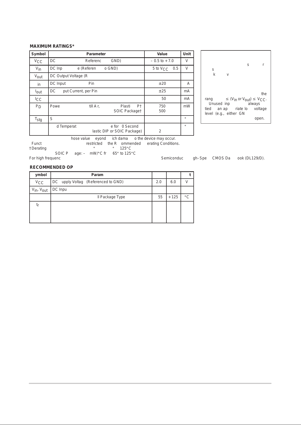
MAXIMUM RATINGS*
Symbol
Parameter
Value
Unit
V
CC
DC Supply Voltage (Referenced to GND)
– 0.5 to + 7.0
V
V
in
DC Input Voltage (Referenced to GND)
– 0.5 to VCC + 0.5
V
V
out
DC Output Voltage (Referenced to GND)
– 0.5 to VCC + 0.5
V
I
in
DC Input Current, per Pin
± 20
mA
I
out
DC Output Current, per Pin
± 25
mA
I
CC
DC Supply Current, VCC and GND Pins
± 50
mA
P
D
Power Dissipation in Still Air, Plastic DIP†
SOIC Package†
750
500
mW
T
stg
Storage Temperature
– 65 to + 150
_
C
ÎÎ
Î
T
L
ОООООООООООО
Î
Lead Temperature, 1 mm from Case for 10 Seconds
(Plastic DIP or SOIC Package)
ÎÎÎ
Î
260
Î
Î
_
C
*Maximum Ratings are those values beyond which damage to the device may occur.
Functional operation should be restricted to the Recommended Operating Conditions.
†Derating — Plastic DIP: – 10 mW/_C from 65_ to 125_C
SOIC Package: – 7 mW/_C from 65_ to 125_C
For high frequency or heavy load considerations, see Chapter 2 of the ON Semiconductor High–Speed CMOS Data Book (DL129/D).
RECOMMENDED OPERATING CONDITIONS
Symbol
Parameter
Min
ÎÎ
Max
Unit
V
CC
DC Supply Voltage (Referenced to GND)
2.0
ÎÎ
6.0
V
Vin, V
out
DC Input Voltage, Output Voltage (Referenced to GND)
0
ÎÎ
V
CC
V
T
A
Operating Temperature, All Package Types
– 55
ÎÎ
+ 125
_
C
ÎÎ
Î
ÎÎ
Î
tr, t
f
ООООООООООООО
Î
ООООООООООООО
Î
Input Rise and Fall Time (Figure 1) VCC = 2.0 V
VCC = 3.0 V
VCC = 4.5 V
VCC = 6.0 V
Î
Î
Î
Î
0
0
0
0
ÎÎ
ÎÎ
ÎÎ
1000
600
500
400
Î
Î
Î
Î
ns
This device contains protection
circuitry to guard against damage
due to high static voltages or electric
fields. However, precautions must
be taken to avoid applications of any
voltage higher than maximum rated
voltages to this high–impedance circuit. For proper operation, Vin and
V
out
should be constrained to the
range GND v (Vin or V
out
) v VCC.
Unused inputs must always be
tied to an appropriate logic voltage
level (e.g., either GND or VCC).
Unused outputs must be left open.
MC74HC161A, MC74HC163A
http://onsemi.com
3
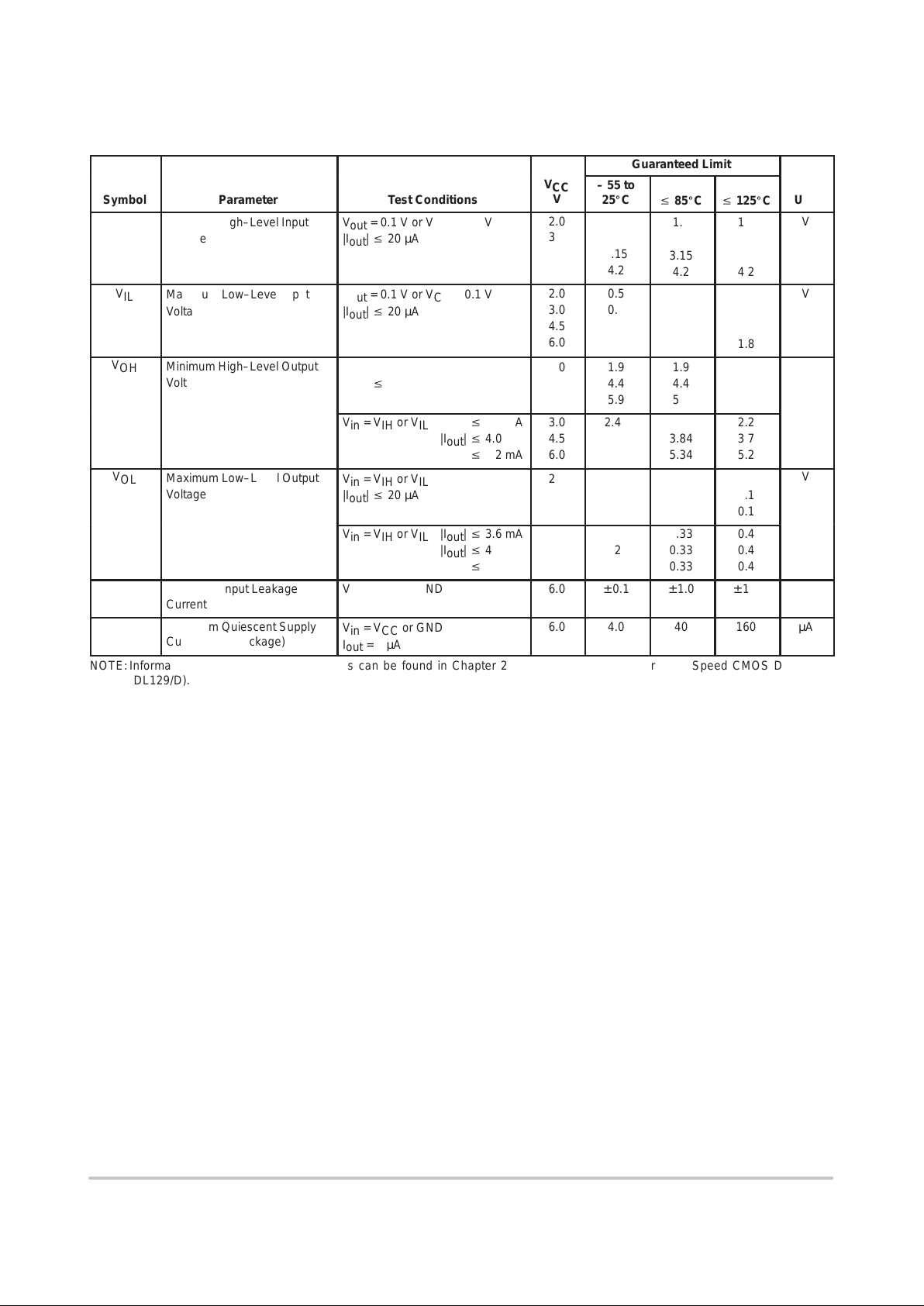
DC ELECTRICAL CHARACTERISTICS (Voltages Referenced to GND)
Guaranteed Limit
Symbol
Parameter
Test Conditions
V
CC
V
– 55 to
25_C
ÎÎÎ
v
85_Cv 125_C
Unit
ÎÎ
Î
ÎÎ
Î
V
IH
ООООООО
Î
ООООООО
Î
Minimum High–Level Input
Voltage
ООООООО
Î
ООООООО
Î
V
out
= 0.1 V or VCC – 0.1 V
|I
out
| v 20 µA
ÎÎ
Î
ÎÎ
Î
2.0
3.0
4.5
6.0
ÎÎ
Î
ÎÎ
Î
1.5
2.1
3.15
4.2
ÎÎÎ
Î
Î
Î
Î
Î
Î
1.5
2.1
3.15
4.2
ÎÎ
Î
ÎÎ
Î
1.5
2.1
3.15
4.2
Î
Î
Î
Î
V
ÎÎ
Î
ÎÎ
Î
ÎÎ
Î
V
IL
ООООООО
Î
ООООООО
Î
ООООООО
Î
Maximum Low–Level Input
Voltage
ООООООО
Î
ООООООО
Î
ООООООО
Î
V
out
= 0.1 V or VCC – 0.1 V
|I
out
| v 20 µA
ÎÎ
Î
ÎÎ
Î
ÎÎ
Î
2.0
3.0
4.5
6.0
ÎÎ
Î
ÎÎ
Î
ÎÎ
Î
0.5
0.9
1.35
1.8
ÎÎÎ
Î
Î
Î
Î
Î
Î
Î
Î
Î
0.5
0.9
1.35
1.8
ÎÎ
Î
ÎÎ
Î
ÎÎ
Î
0.5
0.9
1.35
1.8
Î
Î
Î
Î
Î
Î
V
ÎÎ
Î
V
OH
ООООООО
Î
Minimum High–Level Output
Voltage
ООООООО
Î
Vin = VIH or V
IL
|I
out
| v 20 µA
ÎÎ
Î
2.0
4.5
6.0
ÎÎ
Î
1.9
4.4
5.9
ÎÎÎ
Î
Î
Î
1.9
4.4
5.9
ÎÎ
Î
1.9
4.4
5.9
Î
Î
V
ÎÎÎОООООООÎООООООО
Î
Vin = VIH or VIL|I
out
| v 3.6 mA
|I
out
| v 4.0 mA
|I
out
| v 5.2 mA
ÎÎ
Î
3.0
4.5
6.0
ÎÎ
Î
2.48
3.98
5.48
ÎÎÎ
Î
Î
Î
2.34
3.84
5.34
ÎÎ
Î
2.2
3.7
5.2
Î
Î
ÎÎ
Î
ÎÎ
Î
V
OL
ООООООО
Î
ООООООО
Î
Maximum Low–Level Output
Voltage
ООООООО
Î
ООООООО
Î
Vin = VIH or V
IL
|I
out
| v 20 µA
ÎÎ
Î
ÎÎ
Î
2.0
4.5
6.0
ÎÎ
Î
ÎÎ
Î
0.1
0.1
0.1
ÎÎÎ
Î
Î
Î
Î
Î
Î
0.1
0.1
0.1
ÎÎ
Î
ÎÎ
Î
0.1
0.1
0.1
Î
Î
Î
Î
V
ÎÎÎОООООООÎООООООО
Î
Vin = VIH or VIL|I
out
| v 3.6 mA
|I
out
| v 4.0 mA
|I
out
| v 5.2 mA
ÎÎ
Î
3.0
4.5
6.0
ÎÎ
Î
0.26
0.26
0.26
ÎÎÎ
Î
Î
Î
0.33
0.33
0.33
ÎÎ
Î
0.4
0.4
0.4
Î
Î
ÎÎ
Î
I
in
ООООООО
Î
Maximum Input Leakage
Current
ООООООО
Î
Vin = VCC or GND
ÎÎ
Î
6.0
ÎÎ
Î
± 0.1
ÎÎÎ
Î
Î
Î
± 1.0
ÎÎ
Î
± 1.0
Î
Î
µA
I
CC
Maximum Quiescent Supply
Current (per Package)
Vin = VCC or GND
I
out
= 0 µA
6.0
4.0
ÎÎÎ
40
160
µA
NOTE: Information on typical parametric values can be found in Chapter 2 of the ON Semiconductor High–Speed CMOS Data Book
(DL129/D).
MC74HC161A, MC74HC163A
http://onsemi.com
4
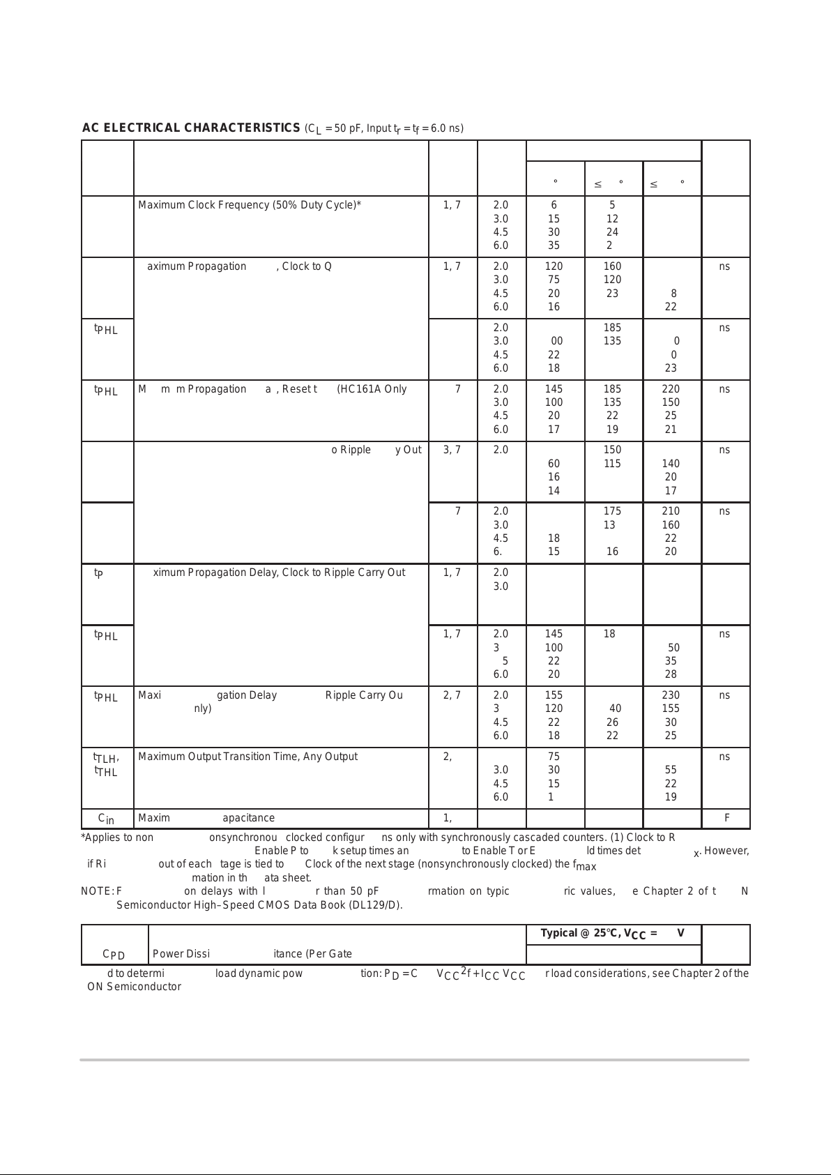
AC ELECTRICAL CHARACTERISTICS (C
L
= 50 pF, Input tr = tf = 6.0 ns)
Guaranteed Limit
ÎÎ
Î
Symbol
ООООООООООООО
Î
Parameter
Î
Î
Fig.
ÎÎ
Î
V
CC
V
ÎÎ
Î
– 55 to
25_C
ÎÎÎ
Î
Î
Î
v
85_C
ÎÎ
Î
v
125_C
Î
Î
Unit
ÎÎ
Î
f
max
ООООООООООООО
Î
Maximum Clock Frequency (50% Duty Cycle)*
Î
Î
1, 7
ÎÎ
Î
2.0
3.0
4.5
6.0
ÎÎ
Î
6
15
30
35
ÎÎÎ
Î
Î
Î
5
12
24
28
ÎÎ
Î
4
10
20
24
Î
Î
MHz
ÎÎ
Î
ÎÎ
Î
t
PLH
ООООООООООООО
Î
ООООООООООООО
Î
Maximum Propagation Delay, Clock to Q
Î
Î
Î
Î
1, 7
ÎÎ
Î
ÎÎ
Î
2.0
3.0
4.5
6.0
ÎÎ
Î
ÎÎ
Î
120
75
20
16
ÎÎÎ
Î
Î
Î
Î
Î
Î
160
120
23
20
ÎÎ
Î
ÎÎ
Î
200
150
28
22
Î
Î
Î
Î
ns
ÎÎ
Î
ÎÎ
Î
t
PHL
ООООООООООООО
Î
ООООООООООООО
Î
Î
Î
Î
Î
1, 7
ÎÎ
Î
ÎÎ
Î
2.0
3.0
4.5
6.0
ÎÎ
Î
ÎÎ
Î
145
100
22
18
ÎÎÎ
Î
Î
Î
Î
Î
Î
185
135
25
20
ÎÎ
Î
ÎÎ
Î
220
150
30
23
Î
Î
Î
Î
ns
ÎÎ
Î
ÎÎ
Î
t
PHL
ООООООООООООО
Î
ООООООООООООО
Î
Maximum Propagation Delay, Reset to Q (HC161A Only)
Î
Î
Î
Î
2, 7
ÎÎ
Î
ÎÎ
Î
2.0
3.0
4.5
6.0
ÎÎ
Î
ÎÎ
Î
145
100
20
17
ÎÎÎ
Î
Î
Î
Î
Î
Î
185
135
22
19
ÎÎ
Î
ÎÎ
Î
220
150
25
21
Î
Î
Î
Î
ns
ÎÎ
Î
ÎÎ
Î
t
PLH
ООООООООООООО
Î
ООООООООООООО
Î
Maximum Propagation Delay, Enable T to Ripple Carry Out
Î
Î
Î
Î
3, 7
ÎÎ
Î
ÎÎ
Î
2.0
3.0
4.5
6.0
ÎÎ
Î
ÎÎ
Î
110
60
16
14
ÎÎÎ
Î
Î
Î
Î
Î
Î
150
115
18
15
ÎÎ
Î
ÎÎ
Î
190
140
20
17
Î
Î
Î
Î
ns
ÎÎ
Î
ÎÎ
Î
t
PHL
ООООООООООООО
Î
ООООООООООООО
Î
Î
Î
Î
Î
3, 7
ÎÎ
Î
ÎÎ
Î
2.0
3.0
4.5
6.0
ÎÎ
Î
ÎÎ
Î
135
100
18
15
ÎÎÎ
Î
Î
Î
Î
Î
Î
175
130
20
16
ÎÎ
Î
ÎÎ
Î
210
160
22
20
Î
Î
Î
Î
ns
ÎÎ
Î
ÎÎ
Î
t
PLH
ООООООООООООО
Î
ООООООООООООО
Î
Maximum Propagation Delay, Clock to Ripple Carry Out
Î
Î
Î
Î
1, 7
ÎÎ
Î
ÎÎ
Î
2.0
3.0
4.5
6.0
ÎÎ
Î
ÎÎ
Î
120
75
22
18
ÎÎÎ
Î
Î
Î
Î
Î
Î
160
135
27
22
ÎÎ
Î
ÎÎ
Î
200
150
30
25
Î
Î
Î
Î
ns
ÎÎ
Î
ÎÎ
Î
t
PHL
ООООООООООООО
Î
ООООООООООООО
Î
Î
Î
Î
Î
1, 7
ÎÎ
Î
ÎÎ
Î
2.0
3.0
4.5
6.0
ÎÎ
Î
ÎÎ
Î
145
100
22
20
ÎÎÎ
Î
Î
Î
Î
Î
Î
185
135
28
24
ÎÎ
Î
ÎÎ
Î
220
150
35
28
Î
Î
Î
Î
ns
ÎÎ
Î
ÎÎ
Î
t
PHL
ООООООООООООО
Î
ООООООООООООО
Î
Maximum Propagation Delay, Reset to Ripple Carry Out
(HC161A Only)
Î
Î
Î
Î
2, 7
ÎÎ
Î
ÎÎ
Î
2.0
3.0
4.5
6.0
ÎÎ
Î
ÎÎ
Î
155
120
22
18
ÎÎÎ
Î
Î
Î
Î
Î
Î
190
140
26
22
ÎÎ
Î
ÎÎ
Î
230
155
30
25
Î
Î
Î
Î
ns
ÎÎ
Î
ÎÎ
Î
t
TLH
,
t
THL
ООООООООООООО
Î
ООООООООООООО
Î
Maximum Output Transition Time, Any Output
Î
Î
Î
Î
2, 7
ÎÎ
Î
ÎÎ
Î
2.0
3.0
4.5
6.0
ÎÎ
Î
ÎÎ
Î
75
30
15
13
ÎÎÎ
Î
Î
Î
Î
Î
Î
95
40
19
16
ÎÎ
Î
ÎÎ
Î
110
55
22
19
Î
Î
Î
Î
ns
C
in
Maximum Input Capacitance
1, 7
—
10
ÎÎÎ
10
10
pF
*Applies to noncascaded/nonsynchronous clocked configurations only with synchronously cascaded counters. (1) Clock to Ripple Carry Out
propagation delays. (2) Enable T or Enable P to Clock setup times and (3) Clock to Enable T or Enable P hold times determine f
max
. However,
if Ripple Carry out of each stage is tied to the Clock of the next stage (nonsynchronously clocked) the f
max
in the table above is applicable.
See Applications information in this data sheet.
NOTE: For propagation delays with loads other than 50 pF, and information on typical parametric values, see Chapter 2 of the ON
Semiconductor High–Speed CMOS Data Book (DL129/D).
Typical @ 25°C, VCC = 5.0 V
C
PD
Power Dissipation Capacitance (Per Gate)*
45
pF
*Used to determine the no–load dynamic power consumption: PD = CPD V
CC
2
f + ICC VCC. For load considerations, see Chapter 2 of the
ON Semiconductor High–Speed CMOS Data Book (DL129/D).
MC74HC161A, MC74HC163A
http://onsemi.com
5
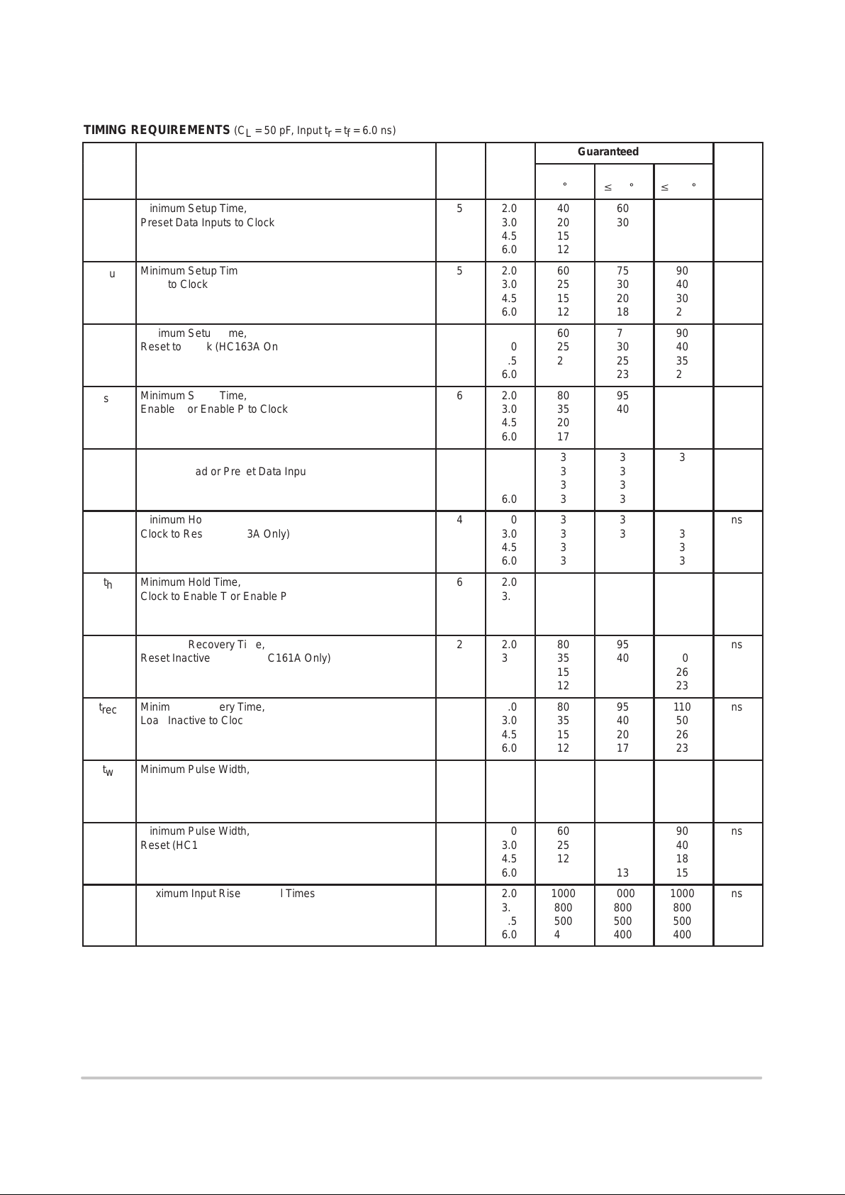
TIMING REQUIREMENTS (C
L
= 50 pF, Input tr = tf = 6.0 ns)
Guaranteed Limit
ÎÎ
Î
Symbol
ООООООООООООО
Î
Parameter
Î
Î
Fig.
ÎÎ
Î
V
CC
V
ÎÎ
Î
– 55 to
25_C
ÎÎÎ
Î
Î
Î
v
85_C
ÎÎ
Î
v
125_C
Î
Î
Unit
ÎÎ
Î
t
su
ООООООООООООО
Î
Minimum Setup Time,
Preset Data Inputs to Clock
Î
Î
5
ÎÎ
Î
2.0
3.0
4.5
6.0
ÎÎ
Î
40
20
15
12
ÎÎÎ
Î
Î
Î
60
30
20
18
ÎÎ
Î
80
40
30
20
Î
Î
ns
ÎÎ
Î
ÎÎ
Î
t
su
ООООООООООООО
Î
ООООООООООООО
Î
Minimum Setup Time,
Load to Clock
Î
Î
Î
Î
5
ÎÎ
Î
ÎÎ
Î
2.0
3.0
4.5
6.0
ÎÎ
Î
ÎÎ
Î
60
25
15
12
ÎÎÎ
Î
Î
Î
Î
Î
Î
75
30
20
18
ÎÎ
Î
ÎÎ
Î
90
40
30
20
Î
Î
Î
Î
ns
ÎÎ
Î
ÎÎ
Î
t
su
ООООООООООООО
Î
ООООООООООООО
Î
Minimum Setup Time,
Reset to Clock (HC163A Only)
Î
Î
Î
Î
4
ÎÎ
Î
ÎÎ
Î
2.0
3.0
4.5
6.0
ÎÎ
Î
ÎÎ
Î
60
25
20
17
ÎÎÎ
Î
Î
Î
Î
Î
Î
75
30
25
23
ÎÎ
Î
ÎÎ
Î
90
40
35
25
Î
Î
Î
Î
ns
ÎÎ
Î
ÎÎ
Î
t
su
ООООООООООООО
Î
ООООООООООООО
Î
Minimum Setup Time,
Enable T or Enable P to Clock
Î
Î
Î
Î
6
ÎÎ
Î
ÎÎ
Î
2.0
3.0
4.5
6.0
ÎÎ
Î
ÎÎ
Î
80
35
20
17
ÎÎÎ
Î
Î
Î
Î
Î
Î
95
40
25
23
ÎÎ
Î
ÎÎ
Î
110
50
35
25
Î
Î
Î
Î
ns
ÎÎ
Î
ÎÎ
Î
t
h
ООООООООООООО
Î
ООООООООООООО
Î
Minimum Hold Time,
Clock to Load or Preset Data Inputs
Î
Î
Î
Î
5
ÎÎ
Î
ÎÎ
Î
2.0
3.0
4.5
6.0
ÎÎ
Î
ÎÎ
Î
3
3
3
3
ÎÎÎ
Î
Î
Î
Î
Î
Î
3
3
3
3
ÎÎ
Î
ÎÎ
Î
3
3
3
3
Î
Î
Î
Î
ns
ÎÎ
Î
ÎÎ
Î
t
h
ООООООООООООО
Î
ООООООООООООО
Î
Minimum Hold Time,
Clock to Reset (HC163A Only)
Î
Î
Î
Î
4
ÎÎ
Î
ÎÎ
Î
2.0
3.0
4.5
6.0
ÎÎ
Î
ÎÎ
Î
3
3
3
3
ÎÎÎ
Î
Î
Î
Î
Î
Î
3
3
3
3
ÎÎ
Î
ÎÎ
Î
3
3
3
3
Î
Î
Î
Î
ns
ÎÎ
Î
ÎÎ
Î
t
h
ООООООООООООО
Î
ООООООООООООО
Î
Minimum Hold Time,
Clock to Enable T or Enable P
Î
Î
Î
Î
6
ÎÎ
Î
ÎÎ
Î
2.0
3.0
4.5
6.0
ÎÎ
Î
ÎÎ
Î
3
3
3
3
ÎÎÎ
Î
Î
Î
Î
Î
Î
3
3
3
3
ÎÎ
Î
ÎÎ
Î
3
3
3
3
Î
Î
Î
Î
ns
ÎÎ
Î
ÎÎ
Î
t
rec
ООООООООООООО
Î
ООООООООООООО
Î
Minimum Recovery Time,
Reset Inactive to Clock (HC161A Only)
Î
Î
Î
Î
2
ÎÎ
Î
ÎÎ
Î
2.0
3.0
4.5
6.0
ÎÎ
Î
ÎÎ
Î
80
35
15
12
ÎÎÎ
Î
Î
Î
Î
Î
Î
95
40
20
17
ÎÎ
Î
ÎÎ
Î
110
50
26
23
Î
Î
Î
Î
ns
ÎÎ
Î
ÎÎ
Î
t
rec
ООООООООООООО
Î
ООООООООООООО
Î
Minimum Recovery Time,
Load Inactive to Clock
Î
Î
Î
Î
5
ÎÎ
Î
ÎÎ
Î
2.0
3.0
4.5
6.0
ÎÎ
Î
ÎÎ
Î
80
35
15
12
ÎÎÎ
Î
Î
Î
Î
Î
Î
95
40
20
17
ÎÎ
Î
ÎÎ
Î
110
50
26
23
Î
Î
Î
Î
ns
ÎÎ
Î
ÎÎ
Î
t
w
ООООООООООООО
Î
ООООООООООООО
Î
Minimum Pulse Width,
Clock
Î
Î
Î
Î
1
ÎÎ
Î
ÎÎ
Î
2.0
3.0
4.5
6.0
ÎÎ
Î
ÎÎ
Î
60
25
12
10
ÎÎÎ
Î
Î
Î
Î
Î
Î
75
30
15
13
ÎÎ
Î
ÎÎ
Î
90
40
18
15
Î
Î
Î
Î
ns
ÎÎ
Î
ÎÎ
Î
t
w
ООООООООООООО
Î
ООООООООООООО
Î
Minimum Pulse Width,
Reset (HC161A Only)
Î
Î
Î
Î
2
ÎÎ
Î
ÎÎ
Î
2.0
3.0
4.5
6.0
ÎÎ
Î
ÎÎ
Î
60
25
12
10
ÎÎÎ
Î
Î
Î
Î
Î
Î
75
30
15
13
ÎÎ
Î
ÎÎ
Î
90
40
18
15
Î
Î
Î
Î
ns
ÎÎ
Î
ÎÎ
Î
tr, t
f
ООООООООООООО
Î
ООООООООООООО
Î
Maximum Input Rise and Fall Times
Î
Î
Î
Î
ÎÎ
Î
ÎÎ
Î
2.0
3.0
4.5
6.0
ÎÎ
Î
ÎÎ
Î
1000
800
500
400
ÎÎÎ
Î
Î
Î
Î
Î
Î
1000
800
500
400
ÎÎ
Î
ÎÎ
Î
1000
800
500
400
Î
Î
Î
Î
ns

MC74HC161A, MC74HC163A
http://onsemi.com
6
FUNCTION DESCRIPTION
The HC161A/163A are programmable 4–bit synchronous
counters that feature parallel Load, synchronous or
asynchronous Reset, a Carry Output for cascading and
count–enable controls.
The HC161A and HC163A are binary counters with
asynchronous Reset and synchronous Reset, respectively .
INPUTS
Clock (Pin 2)
The internal flip–flops toggle and the output count
advances with the rising edge of the Clock input. In addition,
control functions, such as resetting and loading occur with
the rising edge of the Clock input.
Preset Data Inputs P0, P1, P2, P3 (Pins 3, 4, 5, 6)
These are the data inputs for programmable counting.
Data on these pins may be synchronously loaded into the
internal flip–flops and appear at the counter outputs. P0 (Pin
3) is the least–significant bit and P3 (Pin 6) is the
most–significant bit.
OUTPUTS
Q0, Q1, Q2, Q3 (Pins 14, 13, 12, 11)
These are the counter outputs. Q0 (Pin 14) is the
least–significant bit and Q3 (Pin 11) is the most–significant
bit.
Ripple Carry Out (Pin 15)
When the counter is in its maximum state 11 11, this output
goes high, providing an external look–ahead carry pulse that
may be used to enable successive cascaded counters. Ripple
Carry Out remains high only during the maximum count
state. The logic equation for this output is:
Ripple Carry Out = Enable T • Q0 • Q1 • Q2 • Q3
CONTROL FUNCTIONS
Resetting
A low level on the Reset pin (Pin 1) resets the internal
flip–flops and sets the outputs (Q0 through Q3) to a low
level. The HC161A resets asynchronously, and the HC163A
resets with the rising edge of the Clock input (synchronous
reset).
Loading
With the rising edge of the Clock, a low level on Load (Pin
9) loads the data from the Preset Data input pins (P0, P1, P2,
P3) into the internal flip–flops and onto the output pins, Q0
through Q3. The count function is disabled as long as Load
is low.
Count Enable/Disable
These devices have two count–enable control pins:
Enable P (Pin 7) and Enable T (Pin 10). The devices count
when these two pins and the Load pin are high. The logic
equation is:
Count Enable = Enable P • Enable T • Load
The count is either enabled or disabled by the control
inputs according to Table 1. In general, Enable P is a
count–enable control: Enable T is both a count–enable and
a Ripple–Carry Output control.
Table 1. Count Enable/Disable
Control Inputs Result at Outputs
Load Enable P Enable T Q0 – Q3 Ripple Carry Out
H H H Count
L H H No
Count
High when Q0–Q3
are maximum*
X L H No
Count
High when Q0–Q3
are maximum*
X X L No
Count
L
*Q0 through Q3 are maximum when Q3 Q2 Q1 Q0 = 1111.
01234
5
6
7
89101112
13
14
15
OUTPUT STATE DIAGRAMS
Binary Counters

MC74HC161A, MC74HC163A
http://onsemi.com
7
SWITCHING W AVEFORMS
Figure 1. Figure 2.
Figure 3. Figure 4. HC163A Only
Figure 5. Figure 6.
TEST CIRCUIT
Figure 7.
t
r
t
f
V
CC
GND
t
THL
t
TLH
ANY
OUTPUT
90%
50%
10%
90%
50%
10%
CLOCK
t
PLHtPHL
50%
t
PHL
V
CC
GND
V
CC
GND
ANY
OUTPUT
CLOCK
RESET
50%
50%
t
rec
t
r
t
f
V
CC
GND
t
PHL
t
PLH
90%
50%
10%
90%
50%
10%
t
THL
t
TLH
ENABLE T
RIPPLE
CARRY
OUT
CLOCK
RESET
50%
t
su
V
CC
GND
50%
INPUTS
P0, P1,
P2, P3
50%
V
CC
GND
V
CC
GND
GND
50%
50%
LOAD
CLOCK
V
CC
GND
V
CC
GND
ENABLE T
OR
ENABLE P
50%
50%
CLOCK
*Includes all probe and jig capacitance
CL*
TEST POINT
DEVICE
UNDER
TEST
OUTPUT
V
CC
t
w
1/fmax
t
w
t
h
VALID
t
su
t
h
t
su
t
h
t
rec
VALID
t
su
t
h

MC74HC161A, MC74HC163A
http://onsemi.com
8
P0
P1
P2
P3
ENABLE P
ENABLE T
RESET
T0
R
C
C
LOAD
LOAD
P0
Q0 Q0
Q1
Q2
Q3
RIPPLE
CARRY
OUT
VCC= PIN 16
GND = PIN 8
14
The flip–flops shown in the circuit diagrams are Toggle–Enable flip–flops. A Toggle–
Enable flip–flop is a combination of a D flip–flop and a T flip–flop. When loading data from
Preset inputs P0, P1, P2, and P3, the Load signal is used to disable the Toggle input (Tn) of
the flip–flop. The logic level at the Pn input is then clocked to the Q output of the flip–flop
on the next rising edge of the clock.
A logic zero on the Reset device input forces the internal clock (C) high and resets the Q
output of the flip–flop low.
Q0
Q1
Q1
Q2
Q2
Q3
T1
R
C
C
LOAD
LOAD
P1
T2
R
C
C
LOAD
LOAD
P2
T3
R
C
C
LOAD
LOAD
P3
13
12
11
15
3
4
5
6
7
10
1
Figure 8. 4–Bit Binary Counter with Asynchronous Reset
(MC74HC161A)
R
C
C
LOAD
LOAD
CLOCK
LOAD
9
2

MC74HC161A, MC74HC163A
http://onsemi.com
9
Sequence illustrated in waveforms:
1. Reset outputs to zero.
2. Preset to binary twelve.
3. Count to thirteen, fourteen, fifteen, zero, one and two.
4. Inhibit.
RESET (HC161A)
RESET (HC163A)
LOAD
P0
P1
P2
P3
CLOCK (HC161A)
CLOCK (HC163A)
ENABLE P
ENABLE T
Q0
Q1
Q2
Q3
RIPPLE
CARRY
OUT
(ASYNCHRONOUS)
(SYNCHRONOUS)
12 13 14 15 0 1 2
RESET LOAD
COUNT
ENABLES
OUTPUTS
PRESET
DATA
INPUTS
INHIBIT
COUNT
Figure 9. Timing Diagram

MC74HC161A, MC74HC163A
http://onsemi.com
10
P0
P1
P2
P3
ENABLE P
ENABLE T
RESET
T0
R
C
C
LOAD
LOAD
P0
Q0 Q0
Q1
Q2
Q3
RIPPLE
CARRY
OUT
VCC= PIN 16
GND = PIN 8
14
The flip–flops shown in the circuit diagrams are Toggle–Enable flip–flops. A Toggle–
Enable flip–flop is a combination of a D flip–flop and a T flip–flop. When loading data from
Preset inputs P0, P1, P2, and P3, the Load signal is used to disable the Toggle input (Tn) of
the flip–flop. The logic level at the Pn input is then clocked to the Q output of the flip–flop
on the next rising edge of the clock.
A logic zero on the Reset device input forces the internal clock (C) high and resets the Q
output of the flip–flop low.
Q0
Q1
Q1
Q2
Q2
Q3
T1
R
C
C
LOAD
LOAD
P1
T2
R
C
C
LOAD
LOAD
P2
T3
R
C
C
LOAD
LOAD
P3
13
12
11
15
3
4
5
6
7
10
1
9
2
R
C
C
LOAD
LOAD
CLOCK
LOAD
Figure 10. 4–Bit Binary Counter with Synchronous Reset
(MC74HC163A)

MC74HC161A, MC74HC163A
http://onsemi.com
11
INPUTS
OUTPUTS
TO
MORE
SIGNIFICAN
T
STAGES
LOAD
H = COUNT
L = DISABLE
H = COUNT
L = DISABLE
RESET
CLOCK
LOAD P0 P1 P2 P3
ENABLE P
ENABLE T
CLOCK
RQ0Q1Q2
Q3
RIPPLE
CARRY
OUT
LOAD
RESET
CLOCK
ENABLE P
ENABLE T
TYPICAL APPLICATIONS CASCADING
NOTE: When used in these cascaded configurations the clock f
max
guaranteed limits may not apply. Actual performance will depend on
number of stages. This limitation is due to set up times between Enable (Port) and Clock.
LOAD P0 P1 P2 P3
ENABLE P
ENABLE T
CLOCK
RQ0Q1Q2Q3
RIPPLE
CARRY
OUT
LOAD P0 P1 P2 P3
ENABLE P
ENABLE T
CLOCK
RQ0Q1Q2Q3
RIPPLE
CARRY
OUT
INPUTS
OUTPUTS
INPUTS
OUTPUTS
INPUTS INPUTS INPUTS
OUTPUTS OUTPUTS OUTPUTS
TO
MORE
SIGNIFICAN
T
STAGES
LOAD P0 P1 P2 P3
ENABLE P
ENABLE T
CLOCK
RQ0Q1Q2Q3
RIPPLE
CARRY
OUT
LOAD P0 P1 P2 P3
ENABLE P
ENABLE T
CLOCK
RQ0Q1Q2Q3
RIPPLE
CARRY
OUT
LOAD P0 P1 P2 P3
ENABLE P
ENABLE T
CLOCK
RQ0Q1Q2Q3
RIPPLE
CARRY
OUT
Figure 11. N–Bit Synchronous Counters
Figure 12. Nibble Ripple Counter

MC74HC161A, MC74HC163A
http://onsemi.com
12
Figure 13. Modulo–5 Counter
OUTPUT
OPTIONAL BUFFER
FOR NOISE REJECTION
OTHER
INPUTS
RESET
HC163A
Q0
Q1
Q2
Q3
TYPICAL APPLICATIONS VAR YING THE MODULUS
OUTPUT
OPTIONAL BUFFER
FOR NOISE REJECTION
OTHER
INPUTS
RESET
HC163A
Q0
Q1
Q2
Q3
Figure 14. Modulo–11 Counter
The HC163A facilitates designing counters of any modulus with minimal external logic. The output is glitch–free due to
the synchronous Reset.

MC74HC161A, MC74HC163A
http://onsemi.com
13
P ACKAGE DIMENSIONS
PDIP–16
N SUFFIX
CASE 648–08
ISSUE R
MIN MINMAX MAX
INCHES MILLIMETERS
DIM
A
B
C
D
F
G
H
J
K
L
M
S
18.80
6.35
3.69
0.39
1.02
0.21
2.80
7.50
0°
0.51
19.55
6.85
4.44
0.53
1.77
0.38
3.30
7.74
10°
1.01
0.740
0.250
0.145
0.015
0.040
0.008
0.110
0.295
0°
0.020
0.770
0.270
0.175
0.021
0.070
0.015
0.130
0.305
10°
0.040
NOTES:
1. DIMENSIONING AND TOLERANCING PER ANSI
Y14.5M, 1982.
2. CONTROLLING DIMENSION: INCH.
3. DIMENSION L TO CENTER OF LEADS WHEN
FORMED PARALLEL.
4. DIMENSION B DOES NOT INCLUDE MOLD FLASH.
5. ROUNDED CORNERS OPTIONAL.
2.54 BSC
1.27 BSC
0.100 BSC
0.050 BSC
–A
–
B
18
916
F
H
G
D
16 PL
S
C
–T
–
SEATING
PLANE
K
J
M
L
TA0.25 (0.010)
M M
0.25 (0.010) T B A
M
S S
MIN MINMAX MAX
MILLIMETERS INCHES
DIM
A
B
C
D
F
G
J
K
M
P
R
9.80
3.80
1.35
0.35
0.40
0.19
0.10
0°
5.80
0.25
10.00
4.00
1.75
0.49
1.25
0.25
0.25
7°
6.20
0.50
0.386
0.150
0.054
0.014
0.016
0.008
0.004
0°
0.229
0.010
0.393
0.157
0.068
0.019
0.049
0.009
0.009
7°
0.244
0.019
1.27 BSC 0.050 BSC
NOTES:
1. DIMENSIONING AND TOLERANCING PER ANSI
Y14.5M, 1982.
2. CONTROLLING DIMENSION: MILLIMETER.
3. DIMENSIONS A AND B DO NOT INCLUDE
MOLD PROTRUSION.
4. MAXIMUM MOLD PROTRUSION 0.15 (0.006)
PER SIDE.
5. DIMENSION D DOES NOT INCLUDE DAMBAR
PROTRUSION. ALLOWABLE DAMBAR
PROTRUSION SHALL BE 0.127 (0.005) TOTAL
IN EXCESS OF THE D DIMENSION AT
MAXIMUM MATERIAL CONDITION.
1
8
916
–A
–
–B
–
D
16 PL
K
C
G
–T
–
SEATING
PLANE
R X 45°
M
J
F
P 8 PL
0.25 (0.010) B
M M
SOIC–16
D SUFFIX
CASE 751B–05
ISSUE J

MC74HC161A, MC74HC163A
http://onsemi.com
14
Notes

MC74HC161A, MC74HC163A
http://onsemi.com
15
Notes

MC74HC161A, MC74HC163A
http://onsemi.com
16
ON Semiconductor and are trademarks of Semiconductor Components Industries, LLC (SCILLC). SCILLC reserves the right to make changes
without further notice to any products herein. SCILLC makes no warranty , representation or guarantee regarding the suitability of its products for any particular
purpose, nor does SCILLC assume any liability arising out of the application or use of any product or circuit, and specifically disclaims any and all liability ,
including without limitation special, consequential or incidental damages. “Typical” parameters which may be provided in SCILLC data sheets and/or
specifications can and do vary in different applications and actual performance may vary over time. All operating parameters, including “Typicals” must be
validated for each customer application by customer’s technical experts. SCILLC does not convey any license under its patent rights nor the rights of others.
SCILLC products are not designed, intended, or authorized for use as components in systems intended for surgical implant into the body, or other applications
intended to support or sustain life, or for any other application in which the failure of the SCILLC product could create a situation where personal injury or
death may occur. Should Buyer purchase or use SCILLC products for any such unintended or unauthorized application, Buyer shall indemnify and hold
SCILLC and its officers, employees, subsidiaries, affiliates, and distributors harmless against all claims, costs, damages, and expenses, and reasonable
attorney fees arising out of, directly or indirectly , any claim of personal injury or death associated with such unintended or unauthorized use, even if such claim
alleges that SCILLC was negligent regarding the design or manufacture of the part. SCILLC is an Equal Opportunity/Affirmative Action Employer .
PUBLICATION ORDERING INFORMATION
CENTRAL/SOUTH AMERICA:
Spanish Phone: 303–308–7143 (Mon–Fri 8:00am to 5:00pm MST)
Email: ONlit–spanish@hibbertco.com
ASIA/PACIFIC : LDC for ON Semiconductor – Asia Support
Phone: 303–675–2121 (Tue–Fri 9:00am to 1:00pm, Hong Kong Time)
T oll Free from Hong Kong & Singapore:
001–800–4422–3781
Email: ONlit–asia@hibbertco.com
JAPAN: ON Semiconductor, Japan Customer Focus Center
4–32–1 Nishi–Gotanda, Shinagawa–ku, T okyo, Japan 141–8549
Phone: 81–3–5740–2745
Email: r14525@onsemi.com
ON Semiconductor Website: http://onsemi.com
For additional information, please contact your local
Sales Representative.
MC74HC161A/D
NORTH AMERICA Literature Fulfillment:
Literature Distribution Center for ON Semiconductor
P.O. Box 5163, Denver, Colorado 80217 USA
Phone: 303–675–2175 or 800–344–3860 T oll Free USA/Canada
Fax: 303–675–2176 or 800–344–3867 Toll Free USA/Canada
Email: ONlit@hibbertco.com
Fax Response Line: 303–675–2167 or 800–344–3810 T oll Free USA/Canada
N. American Technical Support: 800–282–9855 Toll Free USA/Canada
EUROPE: LDC for ON Semiconductor – European Support
German Phone: (+1) 303–308–7140 (M–F 1:00pm to 5:00pm Munich Time)
Email: ONlit–german@hibbertco.com
French Phone: (+1) 303–308–7141 (M–F 1:00pm to 5:00pm Toulouse T ime)
Email: ONlit–french@hibbertco.com
English Phone: (+1) 303–308–7142 (M–F 12:00pm to 5:00pm UK Time)
Email: ONlit@hibbertco.com
EUROPEAN TOLL–FREE ACCESS*: 00–800–4422–3781
*Available from Germany, France, Italy , England, Ireland
 Loading...