

Motorola MC74F112D, MC74F112J, MC74F112N Datasheet
4-45
FAST AND LS TTL DATA
DUAL JK NEGATIVE
EDGE-TRIGGERED FLIP-FLOP
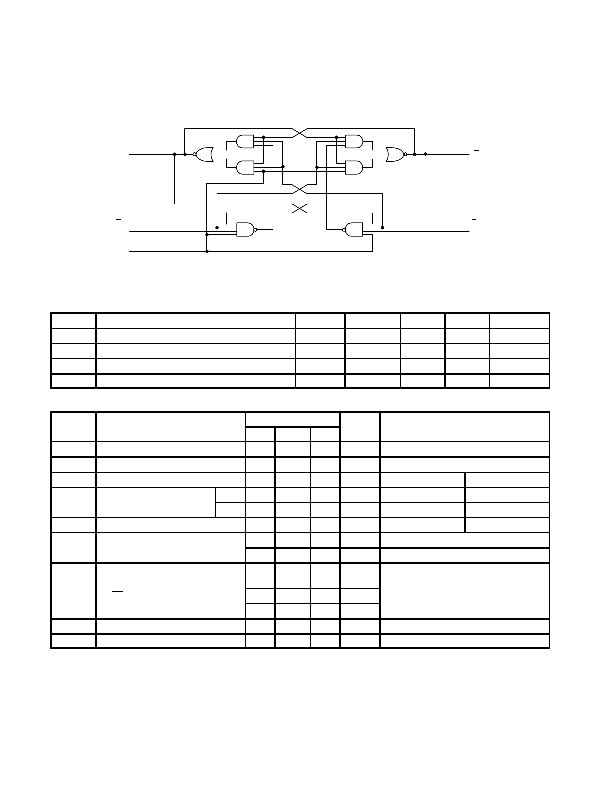
The MC74F1 12 contains two independent, high-speed JK flip-flops with Direct Set and Clear inputs. Synchronous state changes are initiated by the falling edge of the clock. Triggering occurs at a voltage level of the clock and is
not directly related to the transition time. The J and K inputs can change when
the clock is in either state without affecting the flip-flop, provided that they are
in the desired state during the recommended setup and hold times relative to
the falling edge of the clock. A LOW signal on S
D
or CD prevents clocking and
forces Q or Q
HIGH, respectively . Simultaneous LOW signals on S
D
and C
D
force both Q and Q
HIGH.
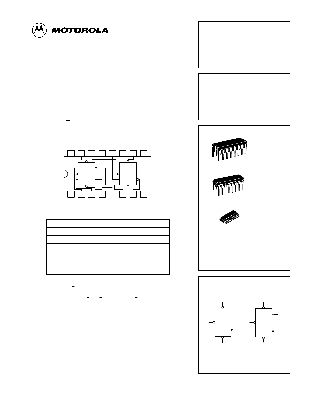
S
D1
21 3 4 6 7 8
GND
CP
1
J
1
K
1
Q1Q1Q
2
5
CP
C
D
CONNECTION DIAGRAM
S
D
J
K Q
1516 14 13 11 10 9
VCCC
D1CD2CP2
J
2
Q
2
12
S
D2
K
2
Q
CP
S
D
C
D
K
J Q
Q
FUNCTION TABLE (Each Half)
Inputs Output
@ t
n
@ tn + 1
J K Q
L L Q
n
L H L
H L H
H H Q
n
H = HIGH Voltage Level
L = LOW Voltage Level
tn = Bit time before clock pulse
tn + 1 = Bit time after clock pulse
J SUFFIX
CERAMIC
CASE 620-09
N SUFFIX
PLASTIC
CASE 648-08
16
1
16
1
16
1
D SUFFIX
SOIC
CASE 751B-03
5
9
MC74FXXXJ Ceramic
MC74FXXXN Plastic
MC74FXXXD SOIC
MC74F112
DUAL JK NEGATIVE
EDGE-TRIGGERED FLIP-FLOP
FAST SCHOTTKY TTL
ORDERING INFORMATION
LOGIC SYMBOL
4
6
1
3
15
10
11
13
7
14
VCC = PIN 16
GND = PIN 8
S
D
J
CP
Q
Q
S
D
J
CP
Q
Q
C
D
2
12
K
K
Asynchronous Inputs:
LOW Input to SD sets Q to HIGH level
LOW Input to CD sets Q to LOW level
Clear and Set are independent of clock
Simultaneous LOW on CD and SD makes both Q and Q HIGH
4-46
FAST AND LS TTL DATA
MC74F112
S
D
Q
K
C
P
C
D
LOGIC DIAGRAM (one half shown)
J
Q
GUARANTEED OPERATING RANGES
Symbol Parameter Min Typ Max Unit
V
CC
Supply Voltage 74 4.5 5.0 5.5 V
T
A
Operating Ambient Temperature Range 74 0 25 70 °C
I
OH
Output Current — High 74 –1.0 mA
I
OL
Output Current — Low 74 20 mA
DC CHARACTERISTICS OVER OPERATING TEMPERATURE RANGE (unless otherwise specified)
Limits
Symbol Parameter Min Typ Max Unit Test Conditions
V
IH
Input HIGH Voltage 2.0 V Guaranteed Input HIGH Voltage
V
IL
Input LOW Voltage 0.8 V Guaranteed Input LOW Voltage
V
IK
Input Clamp Diode Voltage –1.2 V IIN = –18 mA VCC = MIN
74 2.5 3.4 V IOH = –1.0 mA VCC = 4.50 V
V
OH
Output HIGH Voltage 74 2.7 3.4 V IOH = –1.0 mA VCC = 4.75 V
V
OL
Output LOW Voltage 0.35 0.5 V IOL = 20 mA VCC = MIN
I
IH
Input HIGH Current 20 µA VCC = MAX, VIN = 2.7 V
100 µA VCC = MAX, VIN = 7.0 V
Input LOW Current
(J and K Inputs)
–0.6 mA
I
IL
(CP Inputs) –2.4 mA VCC = MAX, VIN = 0.5 V
(C
D
and SD Inputs)
–3.0 mA
I
OS
Output Short Circuit Current (Note 2) –60 –150 mA VCC = MAX, V
OUT
= 0 V
I
CC
Power Supply Current 12 19 mA VCC = MAX, VCP = 0 V
NOTES:
1. For conditions shown as MIN or MAX, use the appropriate value specified under guaranteed operating ranges.
2. Not more than one output should be shorted at a time, nor for more than 1 second.
 Loading...