

Motorola MC68HC812A4CPV8, MC68HC812A4MPV8, MC68HC812A4PV8, MC68HC812A4VPV8 Datasheet
MCM63P631A
1
MOTOROLA FAST SRAM
Product Preview
64K x 32 Bit Pipelined BurstRAM
Synchronous Fast Static RAM
The MCM63P631A is a 2M bit synchronous fast static RAM designed to provide a burstable, high performance, secondary cache for the 68K Family, PowerPC, and Pentium microprocessors. It is organized as 64K words of 32 bits
each. This device integrates input registers, an output register, a 2–bit address
counter, and high speed SRAM onto a single monolithic circuit for reduced parts
count in cache data RAM applications. Synchronous design allows precise cycle
control with the use of an external clock (K). CMOS circuitry reduces the overall
power consumption of the integrated functions for greater reliability.
Addresses (SA), data inputs (DQx), and all control signals except output
enable (G
), sleep mode (ZZ), and Linear Burst Order (LBO) are clock (K) con-
trolled through positive–edge–triggered noninverting registers.
Bursts can be initiated with either ADSP
or ADSC input pins. Subsequent burst
addresses can be generated internally by the MCM63P631A (burst sequence
operates in linear or interleaved mode dependent upon state of LBO
) and con-
trolled by the burst address advance (ADV
) input pin.
Write cycles are internally self–timed and are initiated by the rising edge of the
clock (K) input. This feature eliminates complex off–chip write pulse generation
and provides increased timing flexibility for incoming signals.
Synchronous byte write (SBx
), synchronous global write (SGW), and synchro-
nous write enable SW
are provided to allow writes to either individual bytes or to
all bytes. The four bytes are designated as “a”, “b”, “c”, and “d”. SBa controls
DQa, SBb
controls DQb, etc. Individual bytes are written if the selected byte
writes SBx
are asserted with SW. All bytes are written if either SGW is asserted
or if all SBx
and SW are asserted.
For read cycles, pipelined SRAMs output data is temporarily stored by an
edge–triggered output register and then released to the output buffers at the next
rising edge of clock (K).
The MCM63P631A operates from a 3.3 V power supply, all inputs and outputs
are LVTTL compatible.
• MCM63P631A–117 = 4.5 ns access / 8.5 ns cycle (117 MHz)
MCM63P631A–100 = 4.5 ns access / 10 ns cycle (100 MHz)
MCM63P631A–75 = 7 ns access / 13.3 ns cycle (75 MHz)
MCM63P631A–66 = 8 ns access / 15 ns cycle (66 MHz)
• Single 3.3 V + 10%, – 5% Power Supply
• ADSP
, ADSC, and ADV Burst Control Pins
• Selectable Burst Sequencing Order (Linear/Interleaved)
• Internally Self–Timed Write Cycle
• Byte Write and Global Write Control
• Sleep Mode (ZZ)
• PB1 Version 2.0 Compatible
• Single–Cycle Deselect Timing
• JEDEC Standard 100–Pin TQFP Package
The PowerPC name is a trademark of IBM Corp., used under license therefrom.
Pentium is a trademark of Intel Corp.
This document contains information on a product under development. Motorola reserves the right to change or discontinue this product without notice.
Order this document
by MCM63P631A/D
MOTOROLA
SEMICONDUCTOR TECHNICAL DATA
MCM63P631A
TQ PACKAGE
TQFP
CASE 983A–01
9/30/97
Motorola, Inc. 1997
MCM63P631A
2
MOTOROLA FAST SRAM
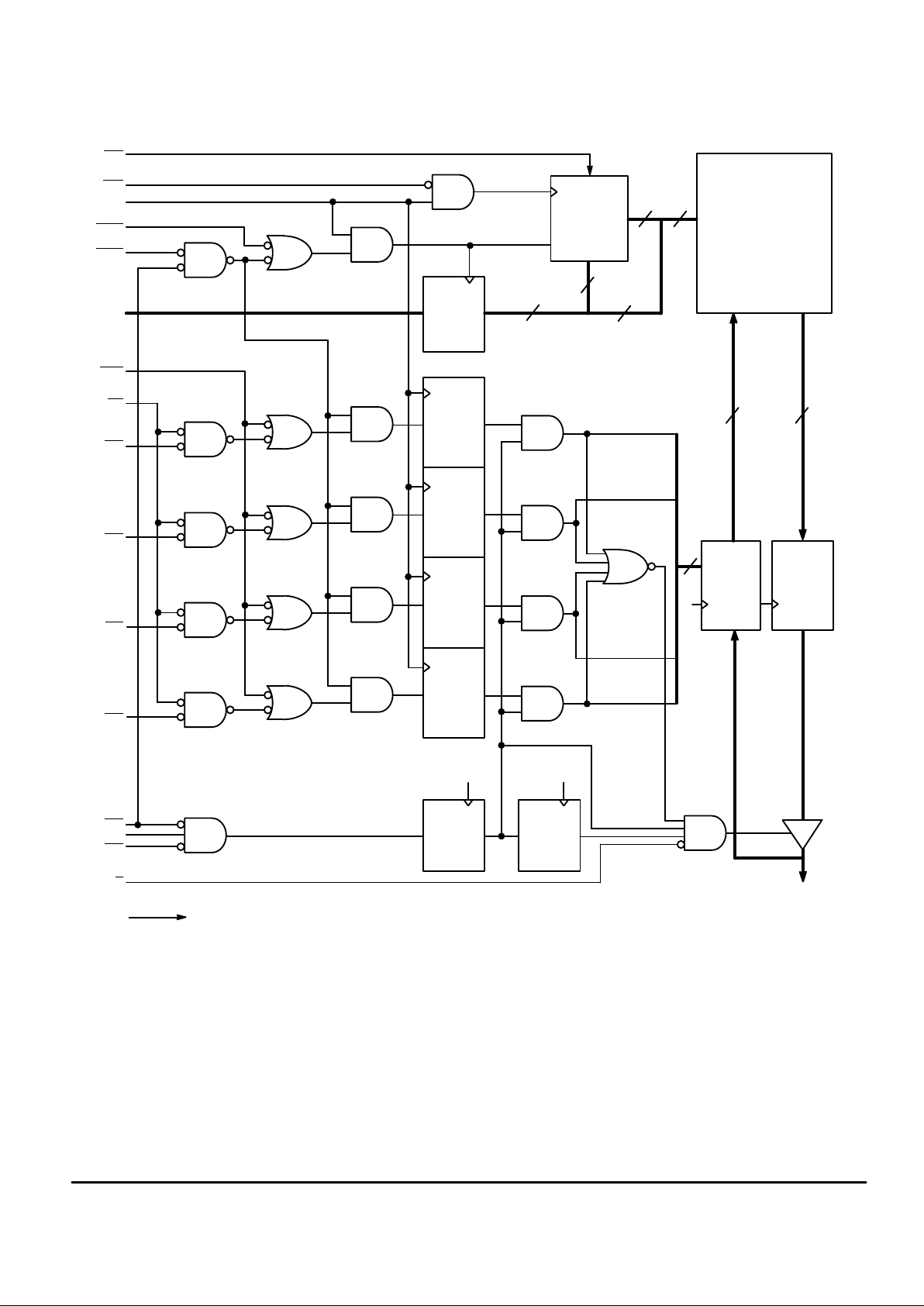
FUNCTIONAL BLOCK DIAGRAM
WRITE
REGISTER
a
WRITE
REGISTER
b
ENABLE
REGISTER
BURST
COUNTER
ADSP
G
CLR
WRITE
REGISTER
c
WRITE
REGISTER
d
SBa
SBb
SBc
SBd
SE3
14
16
SGW
DATA–OUT
REGISTER
ENABLE
REGISTER
K2 K
ADDRESS
REGISTER
16
DATA–IN
REGISTER
64K x 32 ARRAY
SE2
LBO
ADV
K
ADSC
SA
SA1
SA0
SW
SE1
K
4
32
2
2
K2
DQa – DQd
32
ZZ
MCM63P631A
3
MOTOROLA FAST SRAM
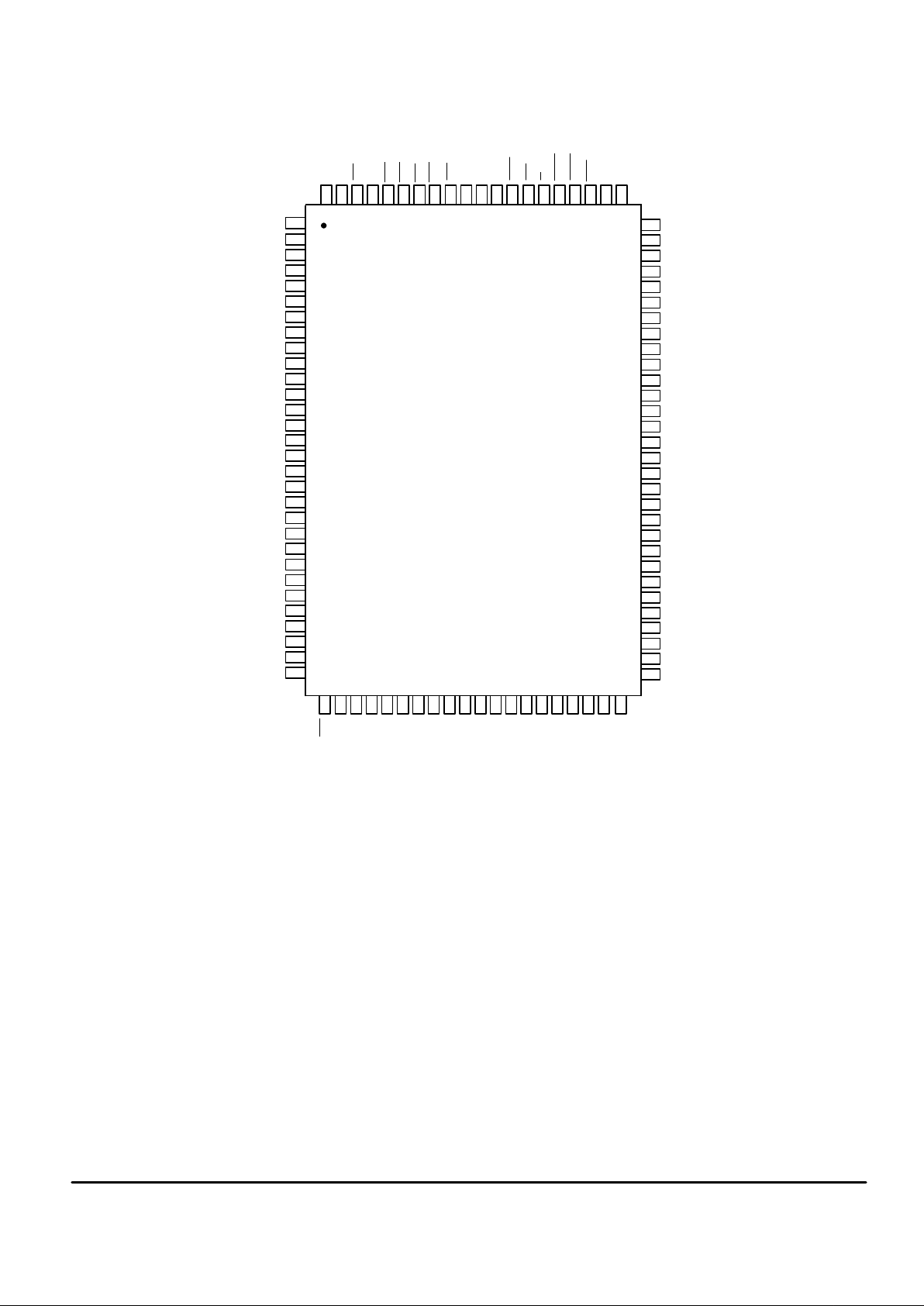
PIN ASSIGNMENT
71
72
DQc
V
DD
NC
69
70
66
67
68
64
65
61
62
63
37 3834 35 36 42 4339 40 41 45 4644
60
59
58
57
56
55
54
53
52
51
31 32 33
74
75
76
77
78
79
80
50494847
DQb
DQb
V
SS
DQb
DQb
DQb
DQb
V
SS
V
DD
DQb
DQb
V
DD
V
SS
V
SS
V
DD
DQc
DQc
DQc
DQc
DQc
DQc
DQc
NC
SASASE1
SBd
K
SBc
ADV
G
ADSC
ADSP
SA0
SASASA
SA
NCNCNC
NC
V
SS
LBO
SA1
V
DD
V
DD
NC
DQa
V
SS
DQa
DQa
DQa
DQa
V
SS
V
DD
DQa
DQa
V
SS
V
DD
NC
DQa
DQd
V
DD
V
SS
V
SS
V
DD
DQd
DQd
DQd
DQd
DQd
73
NC
94 9397 96 95 89 8892 91 90 86 8587100 99 98 81828384
10
9
12
11
15
14
13
17
16
20
19
18
21
22
23
24
25
26
27
28
29
30
7
6
5
4
3
2
1
8
SA
SA
SW
SE2
SBb
SBa
SE3
VSSV
DD
SGW
ZZ
NC
V
DD
V
SS
DQd
DQd
NC
SA
NC
SASASA
SA
SA
MCM63P631A
4
MOTOROLA FAST SRAM
PIN DESCRIPTIONS
Pin Locations Symbol
Type Description
85 ADSC Input Synchronous Address Status Controller: Active low, is used to latch a
new external address. Used to initiate a READ, WRITE or chip
deselect.
84 ADSP Input Synchronous Address Status Processor: Initiates READ or chip
deselect cycle (exception — chip deselect does not occur when ADSP
is asserted and SE1 is high).
83 ADV Input Synchronous Address Advance: Increments address count in
accordance with counter type selected (linear/interleaved).
(a) 52, 53, 56, 57, 58, 59, 62, 63
(b) 68, 69, 72, 73, 74, 75, 78, 79
(c) 2, 3, 6, 7, 8, 9, 12, 13
(d) 18, 19, 22, 23, 24, 25, 28, 29
DQx I/O Synchronous Data I/O: “x” refers to the byte being read or written
(byte a, b, c, d).
86 G Input Asynchronous Output Enable.
89 K Input Clock: This signal registers the address, data in, and all control signals
except G
, LBO, and ZZ.
31 LBO Input Linear Burst Order Input: This pin must remain in steady state (this
signal not registered or latched). It must be tied high or low.
Low — linear burst counter (68K/PowerPC).
High — interleaved burst counter (486/i960/Pentium).
32, 33, 34, 35, 44, 45, 46,
47, 48, 49, 81, 82, 99, 100
SA Input Synchronous Address Inputs: These inputs are registered and must
meet setup and hold times.
36, 37 SA1, SA0 Input Synchronous Address Inputs: These pins must be wired to the two
LSBs of the address bus for proper burst operation. These inputs are
registered and must meet setup and hold times.
93, 94, 95, 96
(a) (b) (c) (d)
SBx Input Synchronous Byte Write Inputs: “x” refers to the byte being written (byte
a, b, c, d). SGW
overrides SBx.
98 SE1 Input Synchronous Chip Enable: Active low to enable chip.
Negated high — blocks ADSP
or deselects chip when ADSC is
asserted.
97 SE2 Input Synchronous Chip Enable: Active high for depth expansion.
92 SE3 Input Synchronous Chip Enable: Active low for depth expansion.
88 SGW Input Synchronous Global Write: This signal writes all bytes regardless of the
status of the SBx
and SW signals. If only byte write signals SBx are
being used, tie this pin high.
87 SW Input Synchronous Write: This signal writes only those bytes that have been
selected using the byte write SBx
pins. If only byte write signals SBx
are being used, tie this pin low.
64 ZZ Input Sleep Mode: This active high asynchronous signal places the RAM into
the lowest power mode. The ZZ pin disables the RAMs internal clock
when placed in this mode. When ZZ is negated, the RAM remains in
low power mode until it is commanded to READ or WRITE. Data
integrity is maintained upon returning to normal operation.
4, 11, 15, 20, 27, 41,
54, 61, 65, 70, 77, 91
V
DD
Supply Power Supply: 3.3 V + 10%, – 5%.
5, 10, 17, 21, 26, 40,
55, 60, 67, 71, 76, 90
V
SS
Supply Ground.
1, 14, 16, 30, 38, 39,
42, 43, 50, 51, 66, 80
NC — No Connection: There is no connection to the chip.
MCM63P631A
5
MOTOROLA FAST SRAM
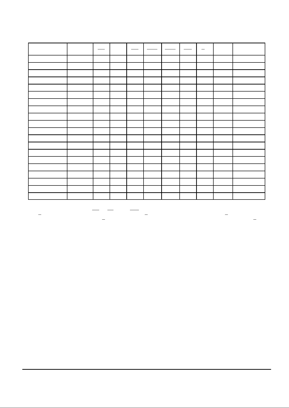
TRUTH TABLE (See Notes 1 through 5)
Next Cycle
Address
Used
SE1 SE2 SE3 ADSP ADSC ADV G
3
DQx Write 2,
4
Deselect None 1 X X X 0 X X High–Z X
Deselect None 0 X 1 0 X X X High–Z X
Deselect None 0 0 X 0 X X X High–Z X
Deselect None X X 1 1 0 X X High–Z X
Deselect None X 0 X 1 0 X X High–Z X
Begin Read External 0 1 0 0 X X X High–Z READ
5
Begin Read External 0 1 0 1 0 X X High–Z READ
5
Continue Read Next X X X 1 1 0 1 High–Z READ
Continue Read Next X X X 1 1 0 0 DQ READ
Continue Read Next 1 X X X 1 0 1 High–Z READ
Continue Read Next 1 X X X 1 0 0 DQ READ
Suspend Read Current X X X 1 1 1 1 High–Z READ
Suspend Read Current X X X 1 1 1 0 DQ READ
Suspend Read Current 1 X X X 1 1 1 High–Z READ
Suspend Read Current 1 X X X 1 1 0 DQ READ
Begin Write External 0 1 0 1 0 X X High–Z WRITE
Continue Write Next X X X 1 1 0 X High–Z WRITE
Continue Write Next 1 X X X 1 0 X High–Z WRITE
Suspend Write Current X X X 1 1 1 X High–Z WRITE
Suspend Write Current 1 X X X 1 1 X High–Z WRITE
NOTES:
1. X = Don’t Care. 1 = logic high. 0 = logic low.
2. Write is defined as either 1) any SBx
and SW low or 2) SGW is low.
3. G
is an asynchronous signal and is not sampled by the clock K. G drives the bus immediately (t
GLQX
) following G going low.
4. On write cycles that follow read cycles, G
must be negated prior to the start of the write cycle to ensure proper write data setup times. G must
also remain negated at the completion of the write cycle to ensure proper write data hold times.
5. This READ assumes the RAM was previously deselected.
 Loading...