

Motorola MC34067P, MC34067DW, MC33067P Datasheet
Order this document by MC34067/D
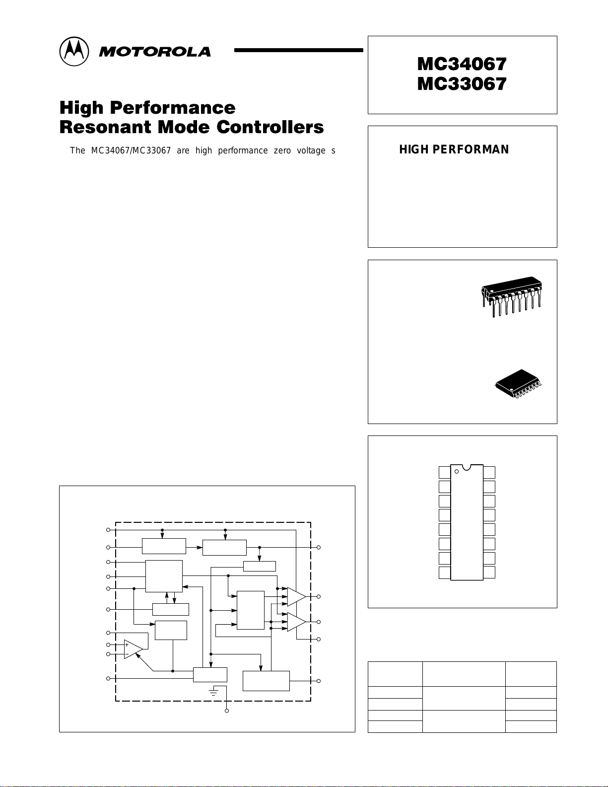
The MC34067/MC33067 are high performance zero voltage switch
resonant mode controllers designed for off–line and dc–to–dc converter
applications that utilize frequency modulated constant off–time or constant
deadtime control. These integrated circuits feature a variable frequency
oscillator, a precise retriggerable one–shot timer, temperature compensated
reference, high gain wide bandwidth error amplifier, steering flip–flop, and
dual high current totem pole outputs ideally suited for driving power
MOSFETs.
Also included are protective features consisting of a high speed fault
comparator and latch, programmable soft–start circuitry, input undervoltage
lockout with selectable thresholds, and reference undervoltage lockout.
These devices are available in dual–in–line and surface mount packages.
• Zero Voltage Switch Resonant Mode Operation
• Variable Frequency Oscillator with a Control Range Exceeding 1000:1
• Precision One–Shot Timer for Controlled Of f–Time
• Internally Trimmed Bandgap Reference
• 4.0 MHz Error Amplifier
• Dual High Current Totem Pole Outputs
• Selectable Undervoltage Lockout Thresholds with Hysteresis
• Enable Input
• Programmable Soft–Start Circuitry
• Low Startup Current for Off–Line Operation
HIGH PERFORMANCE
ZERO VOLTAGE SWITCH
RESONANT MODE
CONTROLLERS
SEMICONDUCTOR
TECHNICAL DATA
P SUFFIX
PLASTIC PACKAGE
CASE 648
DW SUFFIX
PLASTIC PACKAGE
CASE 751G
(SO–16L)
16
1
16
1
Simplified Block Diagram
15
V
CC
Enable /
UVLO Adjust
Osc Charge
Osc RC
Oscillator
Control Current
One–Shot
Error Amp
Output
Noninverting
Input
Inverting Input
Soft–Start
9
1
2
3
16
6
8
7
11
Error
Amp
V
UVLO /
CC
Enable
Variable
Frequency
Oscillator
One–Shot
2.5 V
Clamp
5.0 V
Reference
Soft–Start
MOTOROLA ANALOG IC DEVICE DATA
V
ref
Steering
Flip–Flop
Fault Detector /
Ground4
UVLO
Latch
5
V
ref
14
Output A
12
Output B
13
Pwr Gnd
10
Fault Input
PIN CONNECTIONS
Osc Charge
Osc RC
Osc Control Current
Gnd
V
ref
Error Amp Out
Inverting Input
Noninverting Input
1
2
3
4
5
6
7
8
(Top View)
One–Shot RC
16
V
15
CC
Drive Output A
14
Power Gnd
13
Drive Output B
12
C
11
Soft–Start
Fault Input
10
Enable/UVLO
9
Adjust
ORDERING INFORMATION
Operating
Device
MC34067DW SO–16L
MC34067P Plastic DIP
MC33067DW SO–16L
MC33067P Plastic DIP
Motorola, Inc. 1996 Rev 0
Temperature Range
TA = 0 to + 70°C
TA = – 40° to + 85°C
Package
1
MC34067 MC33067
MAXIMUM RATINGS
Rating Symbol Value Unit
Power Supply Voltage V
Drive Output Current, Source or Sink (Note 1)
Continuous
Pulsed (0.5 µs, 25% Duty Cycle
Error Amplifier, Fault, One–Shot, Oscillator and
Soft–Start Inputs
UVLO Adjust Input V
Power Dissipation and Thermal Characteristics
DW Suffix, Plastic Package, Case 751G
TA = 25°C
Thermal Resistance, Junction–to–Air
P Suffix, Plastic Package, Case 648
TA = 25°C
Thermal Resistance, Junction–to–Air
Operating Junction Temperature T
Operating Ambient Temperature
MC34067
MC33067
Storage Temperature T
CC
I
O
V
in
in(UVLO)
P
D
R
θJA
P
D
R
θJA
J
T
A
stg
20 V
0.3
1.5
– 1.0 to + 6.0 V
– 1.0 to V
862
145
1.25
100
CC
mW
°C/W
W
°C/W
+ 150 °C
°C
0 to + 70
– 40 to + 85
– 55 to + 150 °C
A
V
ELECTRICAL CHARACTERISTICS (V
= 12 V [Note 2], R
CC
OSC
= 18.2 k, R
VFO
= 2940, C
= 300 pF, RT = 2370 k, CT = 300 pF,
OSC
CL = 1.0 nF. For typical values TA = 25°C, for min/max values TA is the operating ambient temperature range that applies [Note 3], unless
otherwise noted.)
Characteristic
Symbol Min Typ Max Unit
REFERENCE SECTION
Reference Output Voltage (IO = 0 mA, TJ = 25°C) V
Line Regulation (VCC = 10 TO 18 V) Reg
Load Regulation (IO = 0 mA to 10 mA) Reg
Total Output Variation Over Line, Load, and Temperature V
Output Short Circuit Current I
Reference Undervoltage Lockout Threshold V
ref
line
load
ref
O
th
5.0 5.1 5.2 V
– 1.0 20 mV
– 1.0 20 mV
4.9 – 5.3 V
25 100 190 mA
3.8 4.3 4.8 V
ERROR AMPLIFIER
Input Offset Voltage (VCM = 1.5 V) V
Input Bias Current (VCM = 1.5 V) I
Input Offset Current (VCM = 1.5 V) I
Open Loop Voltage Gain (VCM = 1.5 V, VO = 2.0 V) A
IO
IB
IO
VOL
– 1.0 10 mV
– 0.2 1.0 µA
– 0 0.5 µA
70 100 – dB
Gain Bandwidth Product (f = 100 kHz) GBW 3.0 5.0 – MHz
Input Common Mode Rejection Ratio (VCM = 1.5 to 5.0 V) CMR 70 95 – dB
Power Supply Rejection Ratio (VCC = 10 to 18 V, f = 120 Hz) PSR 80 100 – dB
Output Voltage Swing
High State
Low State
NOTES: 1. Maximum package power dissipation limits must be observed.
2.Adjust VCC above the Startup threshold before setting to 12 V.
3.Low duty cycle pulse techniques are used during test to maintain junction temperature as close to ambient as possible.
T
=0°C for the MC34067 T
low
=–40°C for the MC33067 T
= + 70°C for MC34067
high
= + 85°C for MC33067
high
V
OH
V
OL
2.8
–
3.2
0.6
–
0.8
V
2
MOTOROLA ANALOG IC DEVICE DATA
MC34067 MC33067
ELECTRICAL CHARACTERISTICS (V
= 12 V [Note 2], R
CC
OSC
= 18.2 k, R
VFO
= 2940, C
= 300 pF, RT = 2370 k, CT = 300 pF,
OSC
CL = 1.0 nF. For typical values TA = 25°C, for min/max values TA is the operating ambient temperature range that applies [Note 3], unless
otherwise noted.)
Characteristic
Symbol Min Typ Max Unit
OSCILLAT OR
Frequency (Error Amp Output Low)
TA = 25°C
Total Variation (VCC = 10 to 18 V, TA = T
Low
to T
High
f
OSC(low)
Frequency (Error Amp Output High)
TA = 25°C
Total Variation (VCC = 10 to 18 V, TA = T
Low
to T
High
f
OSC(high)
Oscillator Control Input Voltage, Pin 3 @ 25°C V
500
490
1900
1850
in
– 2.5 – V
525
–
540
550
2050–2150
2200
kHz
kHz
ONE–SHOT
Drive Output Off–Time
TA = 25°C
Total Variation (VCC = 10 to 18 V, TA = T
Low
to T
High
t
Blank
235
225
250
–
270
280
ns
DRIVE OUTPUTS
Output Voltage
Low State (I
Low State (I
High State (I
High State (I
Output Voltage with UVLO Activated (VCC = 6.0 V, I
= 20 mA)
Sink
= 200 mA)
Sink
Source
Source
= 20 mA)
= 200 mA)
= 1.0 mA) V
Sink
V
V
OL(UVLO)
Output Voltage Rise T ime (CL = 1.0 nF) t
Output Voltage Fall T ime (CL = 1.0 nF) t
OL
OH
r
f
–
–
9.5
9.0
0.8
1.5
10.3
9.7
1.2
2.0
–
–
– 0.8 1.2 V
– 20 50 ns
– 15 50 ns
V
FAULT COMP ARATOR
Input Threshold V
Input Bias Current (V
Propagation Delay to Drive Outputs (100 mV Overdrive) t
= 0 V) I
Pin 10
PLH(In/Out)
th
IB
0.93 1.0 1.07 V
– –2.0 –10 µA
– 60 100 ns
SOFT–START
Capacitor Charge Current (V
Capacitor Discharge Current (V
= 2.5 V) I
Pin 11
= 2.5 V) I
Pin 11
chg
dischg
4.5 9.0 14 µA
3.0 8.0 – mA
UNDERVOLTAGE LOCKOUT
Startup Threshold, VCC Increasing
Enable/UVLO Adjust Pin Open
Enable/UVLO Adjust Pin Connected to V
CC
Minimum Operating Voltage After Turn–On
Enable/UVLO Adjust Pin Open
Enable/UVLO Adjust Pin Connected to V
CC
Enable/UVLO Adjust Shutdown Threshold Voltage V
Enable/UVLO Adjust Input Current (Pin 9 = 0 V) I
V
th(UVLO)
V
CC(min)
th(Enable)
in(Enable)
14.8
8.0
8.0
7.6
16
9.0
9.0
8.6
17.2
10
10
9.6
6.0 7.0 – V
– –0.2 –1.0 mA
V
V
TOTAL DEVICE
Power Supply Current (Enable/UVLO Adjust Pin Open)
Startup (VCC = 13.5 V)
Operating (f
NOTES: 1. Maximum package power dissipation limits must be observed.
2.Adjust VCC above the Startup threshold before setting to 12 V.
3.Low duty cycle pulse techniques are used during test to maintain junction temperature as close to ambient as possible.
T
low
= 500 kHz) (Note 2)
OSC
=0°C for the MC34067 T
=–40°C for the MC33067 T
= + 70°C for MC34067
high
= + 85°C for MC33067
high
I
CC
–
–
0.5
27
0.8
35
mA
MOTOROLA ANALOG IC DEVICE DATA
3
MC34067 MC33067
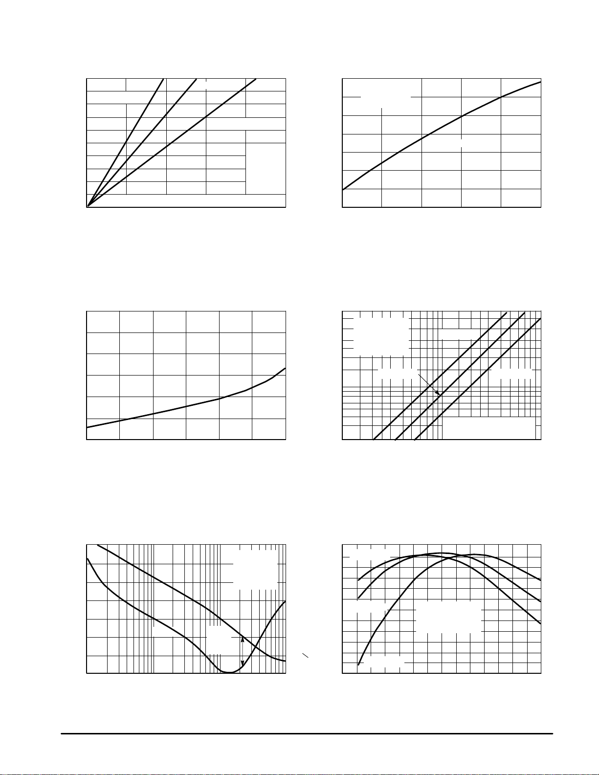
Figure 1. Oscillator Timing Resistor
versus Discharge Time
500
Ω
400
300
200
100
, OSCILLAT OR TIMING RESIST OR (k )
OSC
R
C
= 300 pF
OSC
C
= 200 pF
OSC
C
= 500 pF
OSC
VCC = 12 V
∞
R
=
VFO
RT =
∞
CT = 500 pF
°
C
TA = 25
0
Oscillator Discharge Time is Measured at the Drive Outputs.
t
, OSCILLAT OR DISCHARGE TIME (µs)
dischg
3500
3000
2500
2000
1500
1000
, OSCILLAT OR FREQUENCY (kHz)
500
OSC
f
Figure 3. Error Amp Output Saturation
V oltage versus Oscillator Control Current
0.35
0.30
0.25
0.20
0.15
0.10
, OUTPUT SA TURATION VOLTAGE (V)
sat
V
0.05
0 0.5 1.0 1.5 2.0 2.5 3.0 0.1 0.3 0.6 1.0 3.0 6.0 10
I
, OSCILLAT OR CONTROL CURRENT (mA) tOS, ONE–SHOT PERIOD (
OSC
60
30
Ω
20
10
, TIMING RESISTOR (k )
400
T
R
3.0
Figure 2. Oscillator Frequency versus
Oscillator Control Current
VCC = 12 V
°
C
TA = 25
R
= 18.2 k
OSC
C
= 300 pF
OSC
0
0 400 800 1200 1600 20000 20406080100
I
, OSCILLAT OR CONTROL CURRENT (mA)
OSC
Figure 4. One–Shot Timing Resistor
versus Period
VCC = 12 V
C
= 500 pF
OSC
R
= 100 k
OSC
°
C
TA = 25
CT = 300 pF CT = 500 pF
CT = 200 pF
One–Shot Period is Measured
at the Drive Outputs.
µ
s)
Figure 5. Open Loop V oltage Gain and Phase
versus Frequency
50
Phase
Margin
°
= 64
VCC = 12 V
VO = 2.0 V
RL = 100 k
TA = 25
40
30
20
10
0
, OPEN LOOP VOL TAGE GAIN (dB)
–10
VOL
A
–20
10 k 100 k 1.0M 10M – 55 – 25 0 25 50 75 125100
Gain
Phase
f, FREQUENCY (Hz)
50
60
70
°
C
80
90
100
0, EXCESS PHASE (DEGREES)
110
120
, REFERENCE OUTPUT VOLTAGE CHANGE (mV)
∇
V
4
Figure 6. Reference Output V oltage Change
versus T emperature
*V
= 5.0 V
ref
0
–10
–20
*V
= 5.0 V
–30
–40
–50
ref
ref
*V
= 5.0 V
ref
TA, AMBIENT TEMPERATURE (°C)
VCC = 12 V
∞
RL =
*V
ref at TA
= 25°C
MOTOROLA ANALOG IC DEVICE DATA
MC34067 MC33067
Figure 7. Reference V oltage Change
0
–10
–20
–30
–40
–50
, REFERENCE OUTPUT VOLTAGE CHANGE (mV)
ref
V
∇
VCC = 12 V
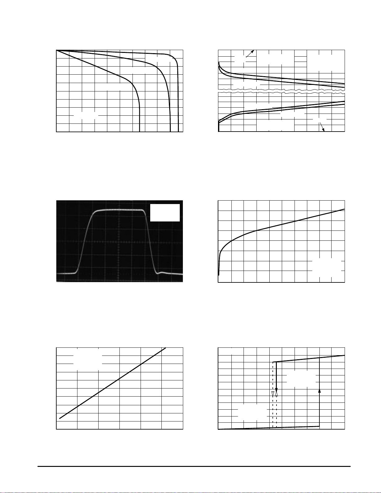
Figure 9. Drive Output Waveform
90%
versus Source Current
TA = – 40°C
TA = – 20°C
TA = –125°C
I
, REFERENCE SOURCE CURRENT (mA)
ref
CL = 1.0 nF
TA = 25
Figure 8. Drive Output Saturation Voltage
versus Load Current
, OUTPUT SA TURATION VOLTAGE (V)
V
sat
–1.0
– 2.0
– 3.0
3.0
2.0
1.0
0
V
CC
TA = 25°C
TA = – 40°C
0
0 0.2 0.4 0.6 0.8 1.00 20 40 60 80 100
Source Saturation
(Load to Ground)
TA = – 40°C
TA = 25°C
Source Saturation
(Load to VCC)
IO, OUTPUT LOAD CURRENT (A)
80
VCC = 12 V
µ
s Pulsed Load
120 Hz Rate
Gnd
Figure 10. Soft–Start Saturation Voltage
versus Capacitor Discharge Current
3.2
°
C
2.4
10%
2000
1600
1200
800
f, FREQUENCY (kHz)
400
20 ns/DIV
Figure 11. Operating Frequency
versus Supply Current
VCC = 12 V
CL = 1.0 nF
°
C
TA = 25
1.6
0.8
OL
0
V , SOFT–START SATURATION VOLTAGE (V)
0 2.0 4.0 6.0 8.0 10
I
, CAPACITOR DISCHARGE CURRENT (mA)
dchg
VCC = 12 V
Pin 10 = V
TA = 25 °C
Figure 12. Supply Current versus Supply V oltage
24
TA = 25 °C
20
Enable/UVLO
Adjust Pin
Open
CC
I , SUPPLY CURRENT (mA)
16
12
8.0
4.0
Enable/UVLO
Adjust Pin
to V
CC
ref
0
30 40 50 60 70 80 90 0 4.0 8.0 12 16 20
ICC, INPUT SUPPLY CURRENT (mA)
0
VCC, SUPPLY VOLTAGE (V)
MOTOROLA ANALOG IC DEVICE DATA
5
 Loading...